
Figures & data
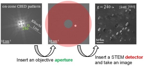
Figure 1. Schematic examples of classification in CTEM mode, where cyan, magenta, and green line below the specimen shows diffraction wave of cyan plane, diffraction wave of magenta plane and transmitted wave, respectively. (a) On-axis and on-zone BF-CTEM. (b) On-axis and off-zone BF-CTEM. (c) On-axis and off-zone DF-CTEM. (d) Off-axis and on-zone DF-CTEM. (e) Off-axis and off-zone DF-CTEM.
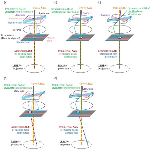
Figure 2. Schematic examples of classification in STEM mode, where cyan, magenta, and green line below the specimen shows diffraction wave of cyan plane, diffraction wave of magenta plane and transmitted wave, respectively. (a) On-axis and on-zone BF-STEM. (b) On-axis and off-zone BF-STEM. (c) On-axis and on-zone DF-STEM. (d) Off-axis and on-zone DF-STEM. (e) Off-axis and off-zone DF-STEM.
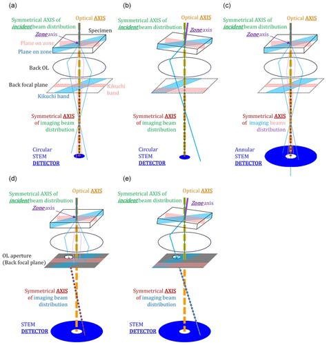
Figure 3. Experimental setup. (a) Ronchigram example taken from amorphous region in TEM specimen of the single crystalline aluminum. The yellow dashed circle shows position example and size of the condenser aperture with a diameter of 10 μm. (b) The result of the condenser aperture insertion. (c) CBED pattern example taken from crystalline region in TEM specimen of the
single crystalline aluminum along the
zone axis. The green dashed circle and blue solid circle shows position example and size of the OL aperture with a diameter of 20 μm and the BF-STEM detector, respectively. (d) The result of the OL aperture insertion to the centre of 044 disk. The red solid circle shows position example and size of the ADF-STEM detector. (e) Schematic of setup for (c). (f) Schematic of setup for (d). (f) Schematic of setup for DsoZ-STEM.
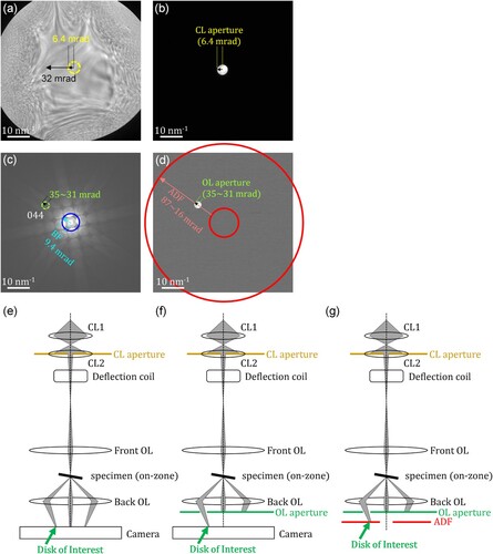
Figure 4. Applicability test of g b invisibility criterion. (a) On zone [001] CBED pattern with the positions and size of inner edge of the ADF-STEM detector (red solid circle), outer edge of the BF-STEM detector (blue solid circle) and the OL aperture (green dashed circle). (b) BF-STEM image. (c) DsoZ-STEM image with [001] zone axis and diffraction disk. (d) DsoZ-STEM image with [001] zone axis and
diffraction disk. The small dislocation marked by orange solid ellipse appears to have a long axis parallel to [
] direction in (b) but is visible in (d) not (c).
![Figure 4. Applicability test of g b invisibility criterion. (a) On zone [001] CBED pattern with the positions and size of inner edge of the ADF-STEM detector (red solid circle), outer edge of the BF-STEM detector (blue solid circle) and the OL aperture (green dashed circle). (b) BF-STEM image. (c) DsoZ-STEM image with [001] zone axis and 4¯40 diffraction disk. (d) DsoZ-STEM image with [001] zone axis and 4¯4¯0 diffraction disk. The small dislocation marked by orange solid ellipse appears to have a long axis parallel to [4¯4¯0] direction in (b) but is visible in (d) not (c).](/cms/asset/bd68f238-f35b-43cb-9e44-d7a028b60b0c/tphl_a_2321134_f0004_oc.jpg)
Table 1. Details of dislocation loops investigated in this study.
Figure 5. Highlighting of dislocation loops utilizing a Kikuchi line. (a) On zone [001] CBED pattern with the positions and size of inner edge of the ADF-STEM detector (red solid circle) and the OL aperture (green dashed circle). The white solid and dashed line shows a position of Kikuchi line of () plane and (
) plane. (b) DsoZ-STEM image with [001] zone axis and
diffraction disk containing defect Kikuchi line of (
) plane. (c) DsoZ-STEM image with [001] zone axis and
diffraction disk containing Kikuchi line of (
) plane. (d) DsoZ-STEM image with [001] zone axis and
diffraction disk. (e) Brightness profile of the selected area A (yellow solid line rectangle in (b)–(d)). The normalized brightness value was calculated by dividing the brightness value by minimum brightness value in the profile. The faint dislocation marked by orange solid line ellipse is visible in (b) and (c) but almost invisible in (d).
![Figure 5. Highlighting of dislocation loops utilizing a Kikuchi line. (a) On zone [001] CBED pattern with the positions and size of inner edge of the ADF-STEM detector (red solid circle) and the OL aperture (green dashed circle). The white solid and dashed line shows a position of Kikuchi line of (2¯20) plane and (22¯0) plane. (b) DsoZ-STEM image with [001] zone axis and 2¯4¯0 diffraction disk containing defect Kikuchi line of (2¯20) plane. (c) DsoZ-STEM image with [001] zone axis and 4¯2¯0 diffraction disk containing Kikuchi line of (22¯0) plane. (d) DsoZ-STEM image with [001] zone axis and 4¯4¯0 diffraction disk. (e) Brightness profile of the selected area A (yellow solid line rectangle in (b)–(d)). The normalized brightness value was calculated by dividing the brightness value by minimum brightness value in the profile. The faint dislocation marked by orange solid line ellipse is visible in (b) and (c) but almost invisible in (d).](/cms/asset/1b3c09ee-814f-4150-add4-28f2594ba1f6/tphl_a_2321134_f0005_oc.jpg)
Figure 6. Visibility confirmation of dislocation line using a specific pair of g. (a) On zone [001] CBED pattern with the positions and size of inner edge of the ADF-STEM detector (red solid circle), outer edge of the BF-STEM detector (blue solid circle) and the OL aperture (green dashed circle). (b) DsoZ-STEM image with [001] zone axis and
diffraction disk. (c) DsoZ-STEM image with [001] zone axis and
diffraction disk. (d) BF-STEM image. (e) Brightness profile of the selected area B (yellow solid line rectangle in (b)–(d)). The normalized brightness value was calculated by dividing the brightness value by maximum brightness value in each profile.
![Figure 6. Visibility confirmation of dislocation line using a specific pair of ±g. (a) On zone [001] CBED pattern with the positions and size of inner edge of the ADF-STEM detector (red solid circle), outer edge of the BF-STEM detector (blue solid circle) and the OL aperture (green dashed circle). (b) DsoZ-STEM image with [001] zone axis and 42¯0 diffraction disk. (c) DsoZ-STEM image with [001] zone axis and 4¯20 diffraction disk. (d) BF-STEM image. (e) Brightness profile of the selected area B (yellow solid line rectangle in (b)–(d)). The normalized brightness value was calculated by dividing the brightness value by maximum brightness value in each profile.](/cms/asset/ed344ac7-bd42-44cd-a4fb-8c8ca859e765/tphl_a_2321134_f0006_oc.jpg)
Figure 7. Visibility confirmation of dislocation loop using a specific pair of g. (a) On zone [001] CBED pattern with the positions and size of inner edge of the ADF-STEM detector (red solid circle), outer edge of the BF-STEM detector (blue solid circle) and the OL aperture (green dashed circle). (b) DsoZ-STEM image with [001] zone axis and
diffraction disk. (c) DsoZ-STEM image with [001] zone axis and
diffraction disk. (d) BF-STEM image. (e) Brightness profile of the selected area C (yellow solid line rectangle in (b)–(d)).
![Figure 7. Visibility confirmation of dislocation loop using a specific pair of ±g. (a) On zone [001] CBED pattern with the positions and size of inner edge of the ADF-STEM detector (red solid circle), outer edge of the BF-STEM detector (blue solid circle) and the OL aperture (green dashed circle). (b) DsoZ-STEM image with [001] zone axis and 420 diffraction disk. (c) DsoZ-STEM image with [001] zone axis and 4¯2¯0 diffraction disk. (d) BF-STEM image. (e) Brightness profile of the selected area C (yellow solid line rectangle in (b)–(d)).](/cms/asset/2f84501e-37bf-450d-b906-850031f7f794/tphl_a_2321134_f0007_oc.jpg)