Figures & data
Figure 1. (a) PPS pixel and (b) two transistors APS layouts and (c) schematic illustration of the all-organic transistor and photosensor combination in APS architecture (only Taps is depicted).
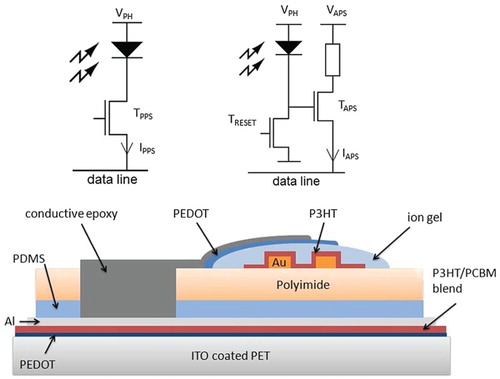
Figure 2. IV characteristics of bulk heterojunction photosensors for different illuminations (EQE in inset).
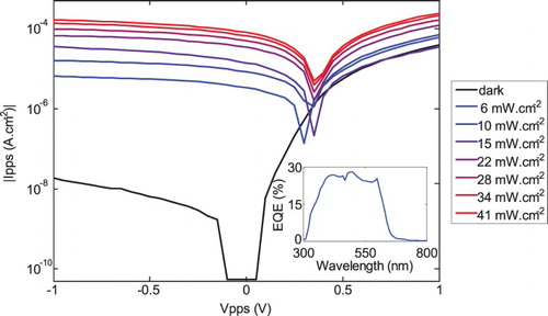
Figure 3. (a) Output characteristics of an UV curable ion-gel OFET (b) Transfer characteristics of an ion-gel dielectric OFET at Vsd = −1 V showing minimal hysteresis and 1 µA maximum leakage current at expected operating voltages. Vg sweep rate was 100 mV s−1.
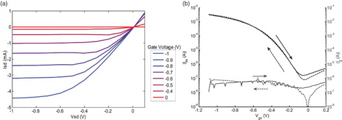
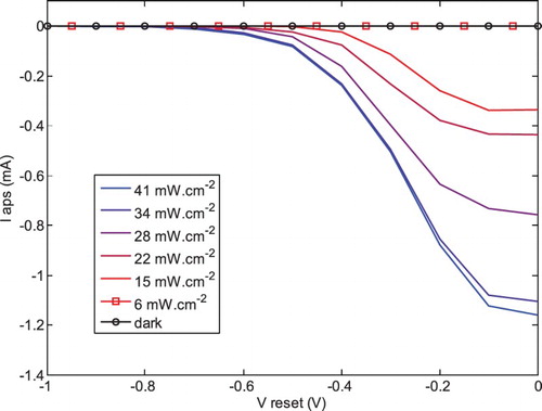
Figure 4. Current Iaps for different photosensor reverse biases Vaps and Treset gate voltages. The maximum Iaps current under dark conditions and 6 mW cm−2 are, respectively, −40 nA and −3.5 µA.