Figures & data
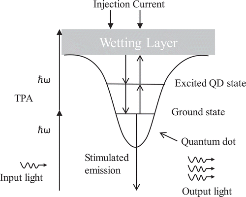
Figure 1. Schematic diagram of the dual SOA-MZI-based XOR gate. BPF: bandpass filter centered at λ2. Two phase shifters are used to induce a π phase difference at two arms.
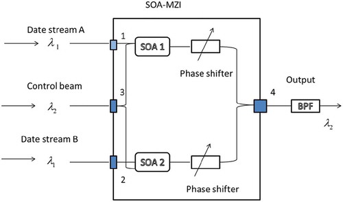
Figure 2. (a) The QD-SOA density of state as a function of transition energy. (b) A schematic of carrier dynamics in an InAs/GaAs QD-SOA. Quantum dots are embedded in the wetting layer.
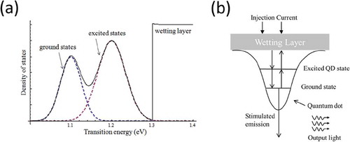
Figure 3. Simulation results of XOR gates operating at 250 Gb/s from a dual QD-SOA MZI scheme.
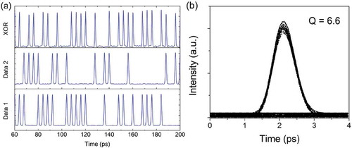
Figure 4. Calculated 250 Gb/s operation quality factor Q at different single pulse energy and transition lifetime from QD excited state to ground state. Injected current density is set to 1.8 kA/cm2. (a): Q factor dependence on single pulse energy, τe-g = 1 ps. (b): Q factor dependence on ES to GS transition lifetime, single pulse energy is 0.5 pJ. Q > 6 is typically needed for bit-error-rate of <10−9. The above figure shows Q > 6 is obtained at 250 Gb/s for pulse width of ~1 ps.
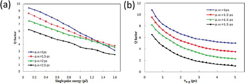
Figure 5. Calculated gain and phase change in an SOA due to a series of pulses shown in (a). (b) Gain modulation as a function of time, (c) phase modulation due to gain modulation as a function of time. The gain plotted is the value of G. (d) total phase modulation including two-photon absorption as a function of time. Note the periodic total phase change is primarily due to two-photon absorption in (d).
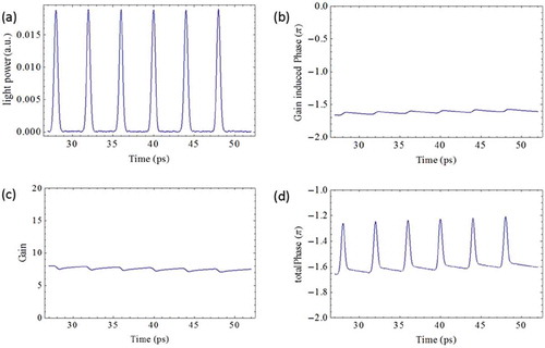
Figure 6. Simulation results of XOR gates operating at 250 Gb/s from a TPA based dual SOA MZI scheme. Data A and Data B are shown on the left. XOR and an eye pattern (after 100 pseudo-random A and B bits) are shown on the right.
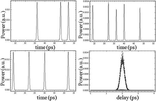
Figure 7. The calculated quality factor Q at different operating bit-rates and different input data stream average powers. Q > 6 is typically needed for bit-error-rate of <10−9. The above figure shows Q > 6 is obtained at 250 Gb/s for input powers of 24 dBm.
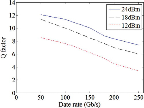
Figure 8. A schematic of carrier dynamics with TPA in an InAs/GaAs QD-SOA.
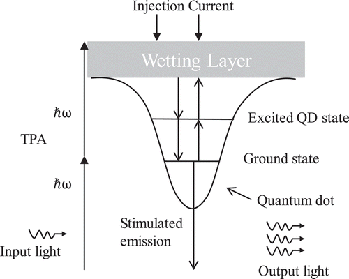
Figure 9. Simulation results of XOR gates operating at 320 Gb/s without the consideration of TPA. The input single pulse energy is 0.5 pJ and pulse width is 1 ps.
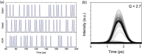
Figure 10. Simulation results of XOR gates operating at 320 Gb/s with the effects of TPA. The input single pulse energy is 0.5 pJ and pulse width is 1 ps.
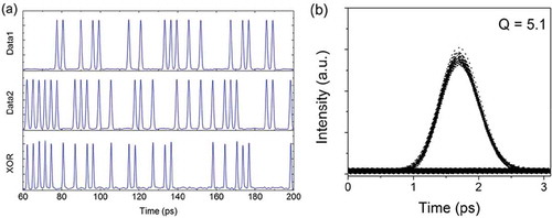
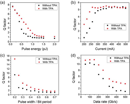
Figure 11. The dependence of Q factor on single pulse energy. The injected current is fixed at 250 mA and pulse width is 1 ps. (b) The dependence of Q factor on injected current. The input single pulse energy is fixed at 0.5 pJ and pulse width is 1 ps. (c) The dependence of Q factor on pulse width/bit period ratio at 320 Gb/s. Note that Q > 6 (needed for bit-error-rate < 10−9) can be obtained. The injected current is fixed at 250 mA and single pulse energy is set at 0.5 pJ. (d) The dependence of Q factor on data rate. The single pulse energy is 0.5 pJ and injected current is 250 mA. The ratio of the pulse width to bit period is fixed.