
Figures & data
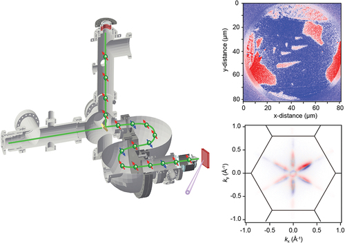
Figure 1. Overview of the iSPEM instrument with the multichannel spin detector. Green lines represent the photoelectron trajectories.
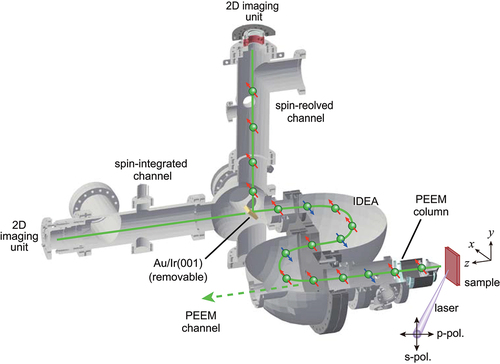
Figure 2. (a) Photoemission microscopy images of poly-Fe scattered by the Au/Ir(001) crystal, where only images at selected scattering energies are shown. (b) IV curves, where Iarea1 and Iarea2 are obtained by the summation of the intensity within the area 1 and area 2 shown in (a), respectively. The asymmetry (c) and the relative FOM (d) obtained by the formulas (7) and (8) are displayed.
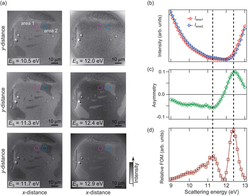
Figure 3. (a) Spin polarization imaging of poly-Fe. The x-spin component is detected. The spin polarization reflecting the magnetic domains in poly-Fe is visualized. Line profiles along #1 (b) and #2 (c) are displayed. Circles give the experimental data. Solid curves represent the fitting results by the step function convoluted with the Gaussian.
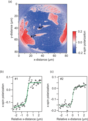
Figure 4. (a) Schematic drawing of the experimental geometry. Light blue parallelogram represents the mirror plane of crystal, which is perpendicular to both the light incident plane and the electric field vector of the light. Spin-integrated (b) and spin-resolved (c) Fermi surface mappings of Bi(111) are shown. Thin solid lines give edges of the surface brillouin zone (SBZ). (d) Spin texture of the spin-polarized surface states for Bi(111) based on the theoretical calculations [Citation48, Citation49]. The arrows represent the spin direction projected in the plane. Here, the information of the spin polarization value is omitted in this figure.
![Figure 4. (a) Schematic drawing of the experimental geometry. Light blue parallelogram represents the mirror plane of crystal, which is perpendicular to both the light incident plane and the electric field vector of the light. Spin-integrated (b) and spin-resolved (c) Fermi surface mappings of Bi(111) are shown. Thin solid lines give edges of the surface brillouin zone (SBZ). (d) Spin texture of the spin-polarized surface states for Bi(111) based on the theoretical calculations [Citation48, Citation49]. The arrows represent the spin direction projected in the plane. Here, the information of the spin polarization value is omitted in this figure.](/cms/asset/e418b73e-c366-4e59-817b-dccb20700891/tstm_a_2328206_f0004_oc.jpg)
Supplemental Material
Download PDF (629.7 KB)Supplemental Material
Download Microsoft Video (AVI) (995.5 KB)Data availability statement
The data that support the findings of this study are available from the corresponding author upon reasonable request.