
Abstract
Surface Acoustic Wave (SAW) aerosol generators, also known as SAW nebulizers or SAW atomizers, are gaining widespread interest in a variety of technical processes due to their ability to produce directed fine mist aerosols with a narrow size distribution and at low shear forces. The interaction of a regulated microscale liquid film with an acoustic wave field on a microfluidic chip surface results in SAW aerosol generation. Future real-world applications require on-chip integrated microfluidic channels for low-cost fabrication of acoustofluidic chips with the required high fluid supply accuracy and reproducibility. In this work, SAW aerosol generation chips employing focused and straight IDTs as well as wafer-scale integrated microfluidic fluid feed channels created by a dry film photoresist multi-stage lamination and lithographic patterning technique were fabricated and validated regarding their performance. The manufactured chips were used with a highly-compact, cost-effective, and easy-to-handle chip holder for experimental studies. Using different SAW chips and liquids, atomization working regimens were determined. The aerosol generator achieved operation at flow rates of 10 μL/min and input power levels of 1 W. The implications of SAW wavelength, IDT type, applied power, liquids, and flow rate on device functionality are explored. Using laser diffraction analysis, it is shown that a simple chip-scale platform is capable of achieving a variable droplet size range. The developed SAW aerosol sources are currently the most advanced demonstrated in the literature and can be used in a variety of technical processes, including mass-spectrometry, olfactory displays, and aerosol-based printing.
Graphical Abstract
Editor:
1. Introduction
In recent years, compact Surface Acoustic Wave (SAW) aerosol generators have gained significant attention in various industrial processes due to their ability to generate fine mist aerosols with a defined droplet size distribution. The driving force of the miniature aerosol generator, known as SAW aerosol generation (also known as SAW nebulization or SAW atomization), is the interaction of a micro-scale liquid film with an acoustic wave field on the surface of a chip. The SAW chip is made from a piezoelectric lithium niobate (128°YX LiNbO3) substrate with interdigital transducers (IDT) for wave field excitation as well as possible functional cover layers. The way the IDT is made, the materials used, the geometry of the fluid supply, and how it is set up in relation to the acoustic wave field all affect how it interacts with the atomized liquid, how long it can be used, and, finally, what properties the aerosol has. Consequently, the design, production, and validation of SAW chips with variable parameters, such as the acoustic wavelength, IDT aperture and type, and the IDT and fluid supply arrangement, is a rather complex and interdisciplinary process that must be performed initially.
Since the SAW fluid interaction is the source of aerosol formation, the position and geometry of the liquid supply in relation to the local acoustic wave field features are essential for predictable and consistent device behavior and aerosol characteristics (Winkler et al. Citation2015). Here, we would like to emphasize that, in our long-term experience, this technique requires a defined liquid supply with a geometry and placement accuracy better than the acoustic wavelength for reproducible and defined aerosol generation. So far, several approaches for liquid feeding to the chip surface have been studied in the literature. Most simply and fundamentally, individual droplets can be introduced to the chip surface via capillaries or tubes (Alvarez et al. Citation2009; Juodkazis and Gu Citation2011; Qi, Yeo, and Friend Citation2008; Yeo and Friend Citation2014). Due to the decrease in droplet volume that occurs during aerosol generation, this approach, however, cannot produce continuous aerosols with constant properties and is therefore not well suited for applications. Also, jetting can occur at the onset of atomization, leading to large droplets (approx. 30–150 µm) in the aerosol. The most common method involves directly placing tissues or capillaries connected to a fluid reservoir on the chip surface (Bllaci et al. Citation2013; Qi et al. Citation2010; Rajapaksa et al. Citation2014; Vuong et al. Citation2013). While this method has proven suitable to investigate the atomization process and demonstrate specialized applications, miniaturization, accuracy, and reproduction remain difficult. Using a glass coverslip to create capillary slits is a third, less prevalent way (Kurosawa et al. Citation1995; Soluch and Wrobel Citation2003, Citation2006). Among the downsides are the complex and time-consuming manual fixations of glass coverslips on the chip surface, the inaccurate slit location in relation to the local features of the acoustic wave field, and restricted control over the precise slit size. Currently, on-chip polymeric SU-8 microchannels represent the most advanced approach for liquid delivery (Kiontke et al. Citation2021; Winkler et al. Citation2015). However, the mechanical stability of these novel SU-8 microchannels is still modest, leading to a reduced chip yield, and the production process is not standard. In addition, several issues must be solved, including channel cover stability, adhesion strength, resistance to delamination, geometrical reproducibility, and scaling to larger wafer sizes. This work is the first to introduce the method of multi-stage lamination of epoxy-based dry film photoresists (DFR) and their lithographic structuring on piezoelectric substrates to solve all of the problems mentioned above, as will be shown in the following.
DFRs are a relatively young class of photoresists available from different producers and involving mainly acrylic- or epoxy-based monomers that can be activated and cross-linked using optical lithography. They typically include three layers: a polyester support base membrane; a resist layer with a thickness ranging from, e.g., 5–150 µm, depending on the material and manufacturer; and a polyolefin sheet on top of the resist, often a 25 µm-thick polyethylene sheet (PET). The dry photoresist is applied via dry lamination, i.e., by uniformly pressing the photoresist across the wafer’s surface with a roll at a controlled pressure and temperature (Kanikella Citation2007). With dry film photoresists, adhesion is typically less critical compared to SU-8 (Dietz Citation2001). Further benefits of DFRs include consistent thickness throughout the entire wafer, high substrate adhesion, simple handling, absence of edge beads, short processing time, reduction of solvent processes during chip fabrication, excellent mechanical stability, and cost-effective production.
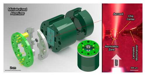
In this study, the electrical and acoustic characteristics of the SAW chip were used to successfully integrate microfluidic channels on the chip at the wafer-scale. This was done using a newly developed multistage lamination technique and lithographic structuring. A custom-made, miniaturized chip holder was realized for aerosol generation studies, considering the exact chip geometries and liquid-feed microchannel positions. The chip holder simplifies the chip exchange procedure, ensures a reproducible rf-electric and fluidic connection, allows efficient heat removal, facilitates cleaning, and shrinks the device’s overall size to the minimum reported so far, i.e., 2.5 cm diameter × 2.6 cm height.
The aerosol generation working regimes for IDTs of different wavelengths and kinds (straight and focused) were investigated using DI water and silver nanoparticle ink. The aerosol generator has been found to accommodate several microliters per minute flow rates with a small input power as low as 1 W. The aerosol sizes were further analyzed using an optical droplet size measurement technique for varied operating conditions. We observed a significant correlation between SAW wavelength, liquid flow rate, and droplet size. The presented comprehensive results facilitate selecting and fabricating an optimal SAW chip design for particular industrial requirements for a given operating mode and droplet size.
2. Material and methods
2.1. Fabrication of SAW aerosol generation chips
SAW aerosol generation chips were manufactured employing optical lithography completely at the wafer-level to provide reliable and consistent production, increase chip yield, and reduce manual handling. The substrate was a four-inch single-side polished (SSP) black 128° YX lithium niobate (LiNbO3) wafer. While SAW-grade black lithium niobate does not show significantly altered performance in SAW excitation and propagation, we use it here due to its reduced pyroelectricity and, hence, lower risk of wafer damage during lab-scale processing. Four lithography layers were constructed utilizing 2D CAD masks. On the cleaned substrates, the liftoff resist AZ 5214E was spin-coated for IDT structuring. After a 3-min soft bake, the resist was exposed using a laser-based mask-less exposure system (MLA 100, Heidelberg Instruments, Heidelberg, Germany). After 2 minutes of image reversal baking and 30 seconds of flood exposure, the film was developed with AZ 726 MIF developer. Subsequently, 5 nm Ti and 295 nm Al were then deposited using electron beam evaporation using custom cluster deposition equipment (Creamet 350 CL6 “Carmen”, CreaVac GmbH, Dresden, Germany), and then lifted using acetone and IPA. A SiO2 target was then used in a reactive rf magnetron sputtering method to create a 500-nm-thick SiO2 layer on the substrate (Creamet 350 CL6). According to IDT production specifications, the liftoff resist was deposited, exposed, and developed. The SiO2 on the contact pads was removed using ion-beam etching (Scia Mill150, Scia Systems GmbH, Chemnitz, Germany).
Laminating dry film photoresist DF3550 was employed for channel shaping (Nagase Chemtex America, LLC., Delaware, OH). For the channel wall structure, the DFR was laminated onto the adhesion-promoted substrate using a manual foil laminator (SKY335R6-31, LMG Germany). Subsequently, this layered substrate was exposed to light using MLA100. They were immersed in cyclohexanone after a post-exposure bake, followed by a hard baking process. For the channel cover structure, the second layer of DF3550 was laminated with a Model 305 laminator (Fortex Engineering, Lincoln, UK). During lamination, PET is peeled first, while the resist remains on the polyester support. After lamination and irradiation, the polyester must be peeled off without separating the resist from the surface. The technique of hot roll lamination produces a dry, smooth contact between the wafer surface and the photopolymer. Similar exposure and a hot plate bake followed for the laminated wafer. After 10 minutes of development in cyclohexanone, the substrate was rinsed, dried, and prepared for dicing. The wafer substrate was diced into chips measuring 14 × 8 mm2. depicts a microfabricated SAW aerosol generation chip, including the structural components.
Figure 1. (a) A SAW aerosol generation chip that features two laminated microchannels and metal IDTs. (b) Assembly schematic of the components of the SAW aerosol generator. c) Aerosol generation in action using the developed SAW aerosol generator.
In the final chip design, the microchannel outputs were positioned centrally between the IDTs and close to the SAW propagation path. The outlets are positioned in locations with low SAW amplitude to prevent excessive heat and heat-induced microchannel wall damage. For establishing liquid film (acoustowetting) creation and subsequent liquid film atomization, the outflow of the channel must be near the propagation path. Therefore, the fluid supply points were located at 25% of the relative wave amplitude for each chip layout, perpendicular to the direction of wave propagation, and a short distance from the IDTs, such as 1-2 mm.
2.2. Chip holder components, fabrications, and setup
All components of our miniaturized chip holder were custom-designed using 3D CAD. depicts the assembly sketch of the aerosol generator’s five individual components: the SAW aerosol generator chip, an rf-suited PCB, a liquid block, the chip holder top part, and the water-cooling bottom part. The circular PCB (custom manufactured by Würth Electronic GmbH & Co. KG, Bangalore, India) offers direct contact with the pads on the chip surface and contains miniaturized MMCX rf connectors, gold-coated spring pins, and 50 °C matched waveguide electrode stripes. A miniaturized rf cable was used to connect the miniaturized rf connector of the PCB to a female SMA connector. The liquid-feeding PEEK block has an O-ring fitting and drilled channels to connect to an external liquid source through PTFE tubing. Without causing damage, the O-ring seals the liquid connection by directly adhering to the DFR channel structures. For the top part of the chip holder, a CNC-manufactured and anodized aluminum platform with a cavity for inserting a heat-conductive foil and the SAW chip was designed, while the bottom part contains a separate water-cooling cavity for efficient heat dissipation. In order to enhance the thermal stability of liquids in the presence of external temperature fluctuations, it is possible to mitigate the adverse effects of parasitic heat through the use of an integrated water-cooling system. In addition, guidance features and stainless-steel guidance pins for the liquid block and the PCB were introduced. The chip is physically and electrically connected to the PCB. The atomizer was specifically engineered for bi-axial installation to ensure compatibility with aerosol printing platforms. depicts the SAW aerosol generator during operation with DI water feed.
2.3. Electrical and acoustical characterization of the SAW chips
Prior to aerosol generation, the rf electrical behavior of the SAW chips was studied in the form of their complex scattering (S) parameters in a frequency range close to the Rayleigh-SAW excitation frequency. The SAW chips were placed in the chip holder and connected to an Agilent Technologies 5070B network analyzer. The network analyzer cables were calibrated up to the point where their male SMA connector met the female SMA connector of the miniaturized rf cable.
Since the acoustic wave field is the dominant boundary condition for the SAW-liquid interaction, the wave field of each individual SAW chip layout was measured around the atomization zone and for various frequencies close to the Rayleigh-SAW excitation frequency using a UHF 120 laser Doppler vibrometer (LDV) (Polytec GmbH, Waldbronn, Germany). Furthermore, the geometry and placement of the liquid supply channels were carefully chosen with respect to the measured SAW amplitude distribution on the chip’s surface to minimize energy uptake in the channel walls while ensuring a defined fluid feed into the SAW propagation path (Winkler et al. Citation2017).
2.4. Aerosol generation and characterization
The general investigations in this study involved aerosol generation experiments with DI water and silver ink at liquid flow rates ranging from 10 to 100 µL/min and total forward electrical power for the SAW atomizer ranging from 0.5 to 6 watts. The particle mass concentration of the silver nanoparticle aqueous spray ink (PSPI-0250 Novacentrix, Austin, TX, USA) was 39%, and it was mixed with DI water at a 1:5 ratio. The viscosity of the silver nanoparticle ink was 25 cP, according to the producer’s data sheet. The choice of silver ink for the experiments conducted in this study was motivated by the significant potential of acoustic microfluidic platforms as a novel additive manufacturing approach for structures at both micro- and macroscales. Our studies include a number of chip configurations, including two IDT types, i.e., straight and focused IDTs (O'Rorke et al. Citation2020), respectively, as well as three wavelengths of 60, 30, and 20 µm. As depicted in , the experimental apparatus included the SAW aerosol generator, stage, syringe pump (neMESYS 290 N, Cetoni GmbH, Korbußen, Germany), signal generator (BSG F20, BelektroniG, Freital, Germany), tiltable stereo-microscope (SMZ-2 T, Nikon Co.), USB camera (TSOUDC3V, Thalheim Spezialoptik GmbH, Pulsnitz, Germany), halogen light source (KL 1500, SCHOTT AG, Mainz, Germany), and laptop.
Figure 2. The apparatus employed in aerosol generation experiments.
Laser diffraction analysis was used to determine the size of the droplets. The droplet size distributions of aerosols from DI water were studied with a Helos KR laser diffractometer (Sympatec GmbH, Clausthal-Zellerfeld, Germany). The measurement of droplet size for the silver nanoparticle ink was not conducted in the laboratory due to safety considerations. The aerosol beam was measured for 3 × 10 s with a laser point about 20 mm in diameter and 25 mm from the chip surface. A suction mechanism was employed to collect the aerosol above the measurement point to prevent liquid condensation on the diffractometer lenses and the recirculation of droplets in the measurement zone. The MIE scattering theory was utilized to compute droplet sizes depending on the refractive index of the supplied liquid.
3. Results and discussions
3.1. Electrical and acoustic characterization
depicts the “excitation curves” of the chip layouts and the driving frequency chosen for this research, which led to the following rf electric device performance assertions: At the ideal working frequencies (S11 minimum) and within a narrow bandwidth, i.e., 64.5 ± 1 MHz, 129 ± 5 MHz, and 196 ± 10 MHz, the SAW devices manufactured are well matched to 50 Ω impedance with a reflection coefficient of power of (Sxx2 < 2%). Reflections at opposing IDTs or chip edges are evident due to frequency-dependent constructive or destructive interference modulating the resonance curve. There are several feasible or useful minima; the selection has, however, for the IDT design used in this study no significant influence on the excited wave field or the aerosol generation behavior if it falls within the minimum zone of the unmodulated curve (see ), as proved by laser-Doppler vibrometry.
Figure 3. (a) Electrical characterization of three impedance-matched standing surface acoustic wave chips with different resonance frequencies in terms of the reflection coefficient magnitude (|S11|). (b) LDV measurement displaying the acoustic wave field profile superimposed over SAW chip microscope pictures for standing SAW with a 20 µm wavelength and 193.5 MHz excitation frequency. (c) Acoustic wave field profile in front of straight and focused IDTs for standing SAW with 30 µm wavelength. The scale bars represent 150 µm.
demonstrates a microscopic image of the standing SAW chip layout with an overlay of the measured amplitude distribution at the optimal driving frequency in the atomization zone. Considering the measured amplitude distribution between two IDTs, the microchannels on the SAW chip can be designed and structured in an optimal manner. The fabrication of the used SAW chips and their configuration are explained in the previous section. Two IDTs of the same kind oppose each other in the SAW chip configuration. To a small extent, the wave field is influenced by reflections of the SAW at the chip edges, which function as mechanical reflectors. In practice, however, variations in their position relative to the IDTs, induced by the dicing process, result only in a slight shift in the modulations of the resonance peak.
This study employs two different IDT designs, namely standard straight and focused IDTs, to compare their aerosol generation performance. To accomplish this, the profile of measured acoustic wave fields in front of both IDTs is characterized and illustrated in . Conventional bidirectional IDTs are widely known and have a simple construction. However, they have drawbacks, such as internal mechanical edge reflections and loss of wave energy on both sides; hence, half of the energy may be wasted in one direction. As depicted in , the focused IDTs concentrate acoustic energy in a narrow region with an almost ideal Gaussian beam profile in the atomization zone, resulting in efficient and targeted actuation with an increased local wave amplitude and thus increased local pressure density in the liquid film (O'Rorke et al. Citation2020).
3.2. General observations of aerosol generation
Typically, liquid atomization by SAWs starts near the exit of the channel after sufficient electrical power is provided to the IDTs, i.e., when a sufficiently high SAW amplitude is reached. Due to standing SAW excitation, aerosols are produced normal on the chip’s surface and form the aerosol plume. As demonstrated in , an increase in the liquid flow rate results in a greater aerosol generation rate and a thicker aerosol plume. In addition, the atomization zone in front of the microchannel might have a larger lateral (wetted) area when the liquid flow rate is increased. The threshold power to atomize the liquid is also flow-rate dependent. Continuous aerosol generation requires greater input power for a higher fluid flow rate. If the supplied SAW amplitude is insufficient, a liquid droplet develops at the exit of the channel. At constant input power, the droplet grows and its behavior is dominated by Eckart streaming, while it may be atomized if the input power is increased significantly. A similar observation has already been reported in an earlier study of ours (Winkler et al. Citation2017).
Figure 4. The observed atomization zone for different parameter settings utilizing DI water: (a) The effect of increasing the liquid flow rate using a 60 µm straight IDTs SAW chip. (b) The effect of increasing forward electrical power with 60 µm focused IDTs and (c) with 20 µm straight IDTs.
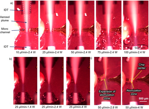
Increased electrical power also broadened the aerosol plume produced by a standing SAW (). This phenomenon may be caused by the increased velocity of the produced droplets as a result of increased forward power, resulting in a wider plume angle. If there is insufficient amplitude to atomize the liquid, as demonstrated in when employing a SAW chip with a 20 µm wavelength, the atomization zone expands in front of the channel exit (as shown in ). Once the local amplitude in front of the channel was insufficient, the liquid film was acoustically steered to a higher amplitude location. When the forward power is increased to 4 W, however, the liquid atomization returns to the chip’s center.
Based on our observations, the focused IDTs used required less energy to atomize the same amount of liquid as the straight IDTs (). Focused IDTs concentrate the amplitude distribution in a tiny region between two transducers, producing a small zone with maximum displacement amplitude, as seen in the figure. Thus, the introduced liquid film acquires the necessary amplitude for atomization in a more effective manner. This leads to the conclusion that inducing very defined acoustic wave fields by focusing IDTs is more energy-efficient and more controlled, particularly in low flow rate arrangements and when portable signal sources provide limited input power.
Figure 5. (a) The observed atomization zone for SAW chips with both focused (1.4 W) and straight (2.4 W) IDTs under identical process conditions. The DI water flow rate was 50 µL/min, and both SAW microfluidics chips have a 60 µm wavelength. (b) The observed atomization zone for a SAW chip with straight (3 W) IDTs when atomizing nanoparticle inks containing silver. The flow rate was 50 µL/min, and the SAW microfluidics chips have a 60 µm wavelength. (c) SAW chips featuring SU-8 and DFR laminated microfluidics channels after the atomization process.
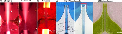
We noticed that the aerosol plume formed with silver nanoparticle ink was less dense than the aerosol plume generated with DI water (). This might be a result of the ink’s high solvent volatility, which the experimental setup under the exhaust hood might have amplified. Using the same SAW device, the input power required for atomizing silver ink was greater than that required for atomizing DI water. This demonstrates that the liquid characteristics and particle content of the ink have a significant impact on liquid disintegration events.
3.3. Comparison of DFR vs. SU-8 approach in SAW aerosol generation
A possible liquid supply technique based on microchannels embedded in SU-8 structures, directly integrated on the chip surface, was previously shown to facilitate mass-scale manufacture of SAW liquid atomizer devices (Winkler et al. Citation2015). The previously employed microchannel structures from SU-8 photoresist and the newly developed structures from laminated DFR after atomization are shown in , for comparison. We noticed fractures on the channel cover as well as the removal/delamination of the channel cover and wall in devices with SU-8 structures (shown with red lines) throughout the experiments we conducted using DI Water. The observed results could perhaps be attributed to the insufficient mechanical stability of SU-8 in the acoustic field region during aerosol production, in addition to adhesion selectivity and resistance striping. The two-wavelength lithography used to structure the channels out of SU-8 allows only a cover thickness of a few µm due to limited light absorption depth. In the case of DFR, a 50 µm cover layer was used, leading to much higher mechanical stability on the vibrating SAW chip surface during the aerosol generation process.
The DFR microchannels were determined to be intact and free of damage after aerosol generation experiments with DI water () and the silver nanoparticle ink. Characteristics of complex fluids, e.g., inks, including liquid viscosity, nanoparticle concentration, and particle size, however, may affect liquid flow in the microchannel, the aerosol properties, and even obstruct the channel. The influence of these properties on the aerosol formation process requires further studies.
3.4. Atomization working regimes
With the help of an optical microscope, the operating regimes of aerosol generation were studied at different liquid flow rates and electrical powers, for two liquids and chips with different wavelengths and IDT types. In these studies, DI water and silver nanoparticle ink were employed at flow rates of 10, 25, 50, 75, and 100 µL/min, while the electrical input power for liquid atomization ranged from 1 to 5 Watt. In , the determined working regimes are shown. The green highlighted zone corresponds to the complete aerosol generation of the supplied liquid, whereas the “No atomization” region reflects settings where atomization was not observed. The points shown in black on the graph denote the individual measurements taken.
Figure 6. The determined atomization regimes for SAW chips with three different IDT wavelengths and (a) straight IDTs and (b) focused IDTs using DI water.
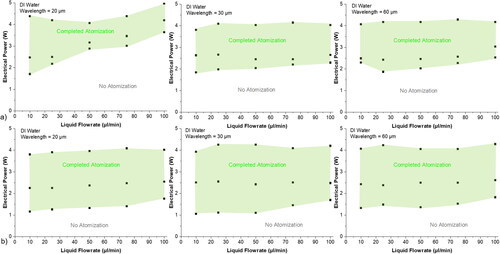
In general, the minimum electrical power required for the formation of aerosols increases as the liquid flow rate increases. This is evident in the operating regimes of devices with shorter wavelengths. For instance, a chip with 20 µm wavelength straight IDTs required roughly 1.7 W of input power to atomize 10 µL/min of DI water, as shown in . However, when the flow rate was increased to 100 µL/min, the input power climbed to around 3.6 W. This could be due to the increased flow rate causing an increase in the liquid film area on the chip surface. This behavior is comparable to that seen by Winkler et al. (Citation2017), who discovered that the liquid flow rate and SAW power can be altered together while retaining stable aerosol generation. Additionally, it has been demonstrated that chips with longer wavelength IDTs require less input power to atomize at greater flow rates. For example, the 60 µm wavelength chip in required only 2.5 W of input power to atomize at a flow rate of 100 µL/min, whereas the 20 µm wavelength chip required approximately 3.6 W of input power under the same conditions. According to the power flow formula, non-linear amplitude dependence on the wavelength is a likely explanation for this phenomenon (Franke et al. Citation2003).
When compared to straight IDTs, focused IDTs seem to require significantly less input power for aerosol generation. As shown in , the onset of aerosol generation in focused IDTs occurs at around 1 W of input power for 10 µL/min, which is lower than in straight IDTs. At a flow rate of 100 µL/min, the 60 µm focused IDT consumes roughly 16% less input power than the 30 µm straight IDT. We observed that the peak amplitude area in the wave field of the focused IDTs is a more confined region where all the energy is concentrated. In comparison, the straight IDTs we applied had a wider amplitude peak (perpendicular to the propagation direction) with less pronounced maxima. To our understanding of the aerosol generation process, the acoustic wave field is its main driving force and can be optimized for energy-efficient aerosol generation for a given fluid and a specific fluid flow rate, e.g., by IDT design.
illustrates the operating regime of the diluted silver nanoparticle ink with a 39% mass concentration utilizing a SAW chip with 60 µm straight IDTs. The input power needed to atomize silver ink was approximately 50% greater than the power necessary to atomize DI water at a flow rate of 50 µL/min. Aerosol generation was unstable at flow rates higher than 75 µL/min, while the SAW chip was operating at a power of 2 Watt and a flow rate of 25 µL/min. This observation may be the result of an increased viscosity in the ink and a greater quantity of liquid in the atomization zone. It should also be mentioned, that an increased viscosity could furthermore lead to more localized dissipation of the acoustic energy (Winkler et al. Citation2016). Understanding the influence of particle concentration on SAW aerosol generation, however, will require additional research in the future. However, this work demonstrates that the SAW aerosol generation process applies to aerosol-based film deposition, even for inks with higher particle concentrations. To our knowledge, so far, no SAW atomization of such highly concentrated ink with such a high flow rate has been presented in the literature.
Figure 7. (a) The determined atomization regimes for a SAW chip with a 60 µm IDT wavelength and straight IDTs using silver nanoparticle ink. The measured droplet size distributions of DI water using a laser diffractometer varied for (b) liquid flow rate, (c) forward electrical power, and (d) acoustic wavelength.
3.5. Aerosol characterization
depict droplet size distributions acquired using laser diffraction with various liquid flow rates and SAW chips. The x-axis represents the mean diameter of the generated droplets, the left y-axis represents the volume fraction, and the right y-axis represents the volume fraction percentage. The measured droplet size distribution of each test is multi-modal, encompassing a peak with extremely small droplet diameters of less than 2.5 µm and a major peak with droplet diameters between 2.5 and 32.5 µm. The first peak, however, is partially outside the detection limit of the laser diffraction technique used and hence could not be studied correctly. After inspecting several distribution functions, we found that the main peak of the experimental data fits the log-normal distribution. The log-normal mean diameter (D) and standard deviation (SD) were determined and used to compare the impact of the various process parameters.
At constant input power, the SAW chip generates larger droplets as the flow rate increases. For instance, the chip with a 60 µm wavelength () produced maximum droplets with a mean diameter of 11.9 µm at a flow rate of 10 µL/min, while the peak was recorded at a mean diameter of 12.1 µm at a flow rate of 25 µL/min, 12.5 µm at a flow rate of 50 µL/min, and 14.4 µm when the flow rate was increased to 75 µL/min. This confirms the conclusion of a previous study that the droplet size distribution was primarily influenced by the liquid flow rate (Winkler et al. Citation2015). The coefficient of variation decreases from 4% at a flow rate of 10 µL/min to 2.5% at a flow rate of 75 µL/min. The coefficient of variation is a relative measure of variability that expresses the SD as a percentage of the mean. It suggests a decrease in variability relative to the mean as liquid throughput increases.
compares the droplet size distributions achieved with an IDT with a 60 µm wavelength under different input powers. The rise in forward electrical power does not significantly impact the distribution of droplet sizes in an identifiable manner. The results are consistent with a previous study’s conclusion that the liquid film geometry approaches an asymptotic limit at higher powers, hence diminishing its influence on the droplet sizes when the power is increased further (Collins et al. Citation2012; Winkler et al. Citation2017). The coefficient of variation rises from 2.8% at 2.4 W to 3.2% at 1.4 W, showing a slight increase in variability compared to the mean as the electrical power increases.
The aerosol generator with a shorter SAW wavelength creates significantly smaller droplets at a given liquid flow rate and input electrical power. As can be seen in , the average droplet size decreases as the wavelength decreases. The 20 µm wavelength chip generated droplets with a size range of 1.5–10 µm and a mean diameter of 4.5 µm, whereas the 60 µm wavelength chip produced droplets with a size range of 2.5–27.5 µm and a mean diameter of 11.9 µm. This validates the findings of a prior investigation, which determined that the distribution of droplet sizes was predominantly affected by the wavelength of the SAW devices (Ju et al. Citation2008). As discussed in our recent studies (Roudini et al. Citation2023; Roudini et al. Citation2020), the local origins of the droplets in SAW aerosol generation are induced droplet-shaped liquid patterns on the chip surface. In SAW chips with a smaller wavelength, smaller fluid patterns are expected to form, leading to disintegrated droplets with reduced diameters by involved aerosol generation mechanisms. This is a significant finding since it shows that a simple chip-scale platform can achieve an adjustable droplet size range.
4. Conclusions
In this study, the fabrication and validation of SAW chips produced using a dry film photoresist technology for wafer-scale on-chip integration of microfluidic channels have been shown. The acoustic and electrical features of the SAW chip designs with varying wavelengths, IDT types, and microchannel geometries were characterized. A highly compact and versatile demonstrator, including a water-cooling component corresponding to the new chip layouts, was designed and prepared. This aerosol generator makes it easy to tailor the atomization process to a certain application, liquid, and flow rate, respectively, simply by swapping in a SAW chip with the appropriate IDT type and wavelength. The atomizer was specifically engineered for bi-axial installation to ensure compatibility with aerosol printing platforms. The new chip production approach thereby enables a truly off-the-shelf approach for SAW atomization chips produced on the wafer scale with high yield using standard methods.
The developed SAW aerosol generator setup was used with variations of process parameters. In addition to identifying the atomization operating regimes for the intended IDTs with various wavelengths and types, the atomization zone on the SAW chips was optically inspected during aerosol generation experiments. Utilizing laser diffraction, the droplets produced by the SAW aerosol generator using DI water were measured. We noticed a substantial relationship between the SAW wavelength and the liquid flow rate and droplet size.
The micro-acoustic liquid aerosol generator proposed in this study is, in summary, energy-efficient, versatile, cost-effective, and simple to use. It can accommodate flow rates as low as 10 µL/min and input power to the SAW atomizer as low as 1 W. After aerosol generation experiments, the intact DFR-laminated microchannels make the SAW microfluidics chip reusable. Depending on the application, liquid to be used, and needed flow rate, a SAW chip with the optimal IDT type and wavelength may conveniently be employed to modify the resultant droplet size distributions by in-situ alteration of liquid flow rates and ex-situ improved chip designs. As the production of the SAW chips is based on rapid prototyping optical laser lithography and dry film lamination, a very fast realization of new chip layouts matched to the needs of a specific application is possible. Moreover, the comprehensive data provided regarding working regimes facilitates the selection and fabrication of the optimal SAW chip design for particular industrial requirements for the operating mode and droplet size.
Disclosure statement
No potential conflict of interest was reported by the author(s).
Additional information
Funding
References
- Alvarez, M., L. Y. Yeo, J. R. Friend, and M. Jamriska. 2009. Rapid production of protein-loaded biodegradable microparticles using surface acoustic waves. Biomicrofluidics 3 (1):14102. doi: 10.1063/1.3055282.
- Bllaci, L., S. Kjellström, L. Eliasson, J. R. Friend, L. Y. Yeo, and S. Nilsson. 2013. Fast surface acoustic wave-matrix-assisted laser desorption ionization mass spectrometry of cell response from islets of Langerhans. Anal. Chem. 85 (5):2623–9. doi: 10.1021/ac3019125.
- Collins, D. J., O. Manor, A. Winkler, H. Schmidt, J. R. Friend, and L. Y. Yeo. 2012. Atomization off thin water films generated by high-frequency substrate wave vibrations. Phys. Rev. E Stat. Nonlin. Soft Matter Phys. 86 (5 Pt 2):056312. doi. doi: 10.1103/PhysRevE.86.056312.
- Dietz, K. H. 2001. Dry film photoresist processing technology. Port Erin, Isle of Man: Electrochemical Publications Limited.
- Franke, K., M. Ross-Messemer, A. Menck, F. S. Hoeller, H. Schmidt, and M. Weihnacht. 2003. The highly sensitive optical measurement of absolute saw amplitudes for power flow analysis. IEEE Trans. Ultrason. Ferroelectr. Freq. Control. 50 (1):77–80. doi. doi: 10.1109/tuffc.2003.1176527.
- Ju, J., Y. Yamagata, H. Ohmori, and T. Higuchi. 2008. High-frequency surface acoustic wave atomizer. Sens. Actuat. A 145–146:437–41. doi: 10.1016/j.sna.2008.01.001.
- Juodkazis, S., and M. Gu. 2011. Smart nano-micro materials and devices. SPIE. 8204.
- Kanikella, P. R. 2007. Process development and applications of a dry film photoresist. Masters Theses. 6821.
- Kiontke, A., M. Roudini, S. Billig, A. Fakhfouri, A. Winkler, and C. Birkemeyer. 2021. Surface acoustic wave nebulization improves compound selectivity of low-temperature plasma ionization for mass spectrometry. Sci. Rep. 11 (1):2948– doi: 10.1038/s41598-021-82423-w.
- Kurosawa, M., T. Watanabe, A. Futami, and T. Higuchi. 1995. Surface acoustic wave atomizer. Sens. Actuat. A 50 (1–2):69–74. doi: 10.1016/0924-4247(96)80086-0.
- O'Rorke, R., A. Winkler, D. Collins, and Y. Ai. 2020. Slowness curve surface acoustic wave transducers for optimized acoustic streaming. RSC Adv. 10 (20):11582–9. doi: 10.1039/C9RA10452F.
- Qi, A., L. Yeo, J. Friend, and J. Ho. 2010. The extraction of liquid, protein molecules and yeast cells from paper through surface acoustic wave atomization. Lab Chip. 10 (4):470–6. doi: 10.1039/b915833b.
- Qi, A., L. Y. Yeo, and J. R. Friend. 2008. Interfacial destabilization and atomization driven by surface acoustic waves. Phys. Fluids 20 (7):074103. doi: 10.1063/1.2953537.
- Rajapaksa, A., A. Qi, L. Y. Yeo, R. Coppel, and J. R. Friend. 2014. Enabling practical surface acoustic wave nebulizer drug delivery via amplitude modulation. Lab Chip. 14 (11):1858–65. doi: 10.1039/c4lc00232f.
- Roudini, M., Juan, O. Manor, C.-D. Ohl, and A. Winkler. 2023. Acoustic resonance effects and cavitation in saw aerosol generation. UltrasonSonochem. 106530. doi: 10.1016/j.ultsonch.2023.106530.
- Roudini, M., D. Niedermeier, F. Stratmann, and A. Winkler. 2020. Droplet generation in standing-surface-acoustic-wave nebulization at controlled air humidity. Phys. Rev. Appl.14 (1):014071. doi: 10.1103/PhysRevApplied.14.014071.
- Soluch, W., and T. Wrobel. 2003. Continuous operation of saw atomiser. Electron. Lett. 39 (6):582–3. doi. doi: 10.1049/el:20030306.
- Soluch, W., and T. Wrobel. 2006. Low driving power saw atomiser. Electron. Lett. 42 (24):1432– doi. doi: 10.1049/el:20062776.
- Vuong, T., A. Qi, M. Muradoglu, B. H. P. Cheong, O. W. Liew, C. X. Ang, J. Fu, L. Yeo, J. Friend, and T. W. Ng. 2013. Precise drop dispensation on superhydrophobic surfaces using acoustic nebulization. Soft Matter. 9 (13):3631–9. doi. doi: 10.1039/c3sm00016h.
- Winkler, A., P. Bergelt, L. Hillemann, and S. Menzel. 2016. Influence of viscosity in fluid atomization with surface acoustic waves. OJA. 06 (03):23–33. doi: 10.4236/oja.2016.63003.
- Winkler, A., S. Harazim, D. J. Collins, R. Brünig, H. Schmidt, and S. B. Menzel. 2017. Compact saw aerosol generator. Biomed. Microdevices. 19 (1):9. doi: 10.1007/s10544-017-0152-9.
- Winkler, A., S. Harazim, S. Menzel, and H. Schmidt. 2015. Saw-based fluid atomization using mass-producible chip devices. Lab Chip. 15 (18):3793–9. doi: 10.1039/c5lc00756a.
- Yeo, L. Y., and J. R. Friend. 2014. Surface acoustic wave microfluidics. Annu. Rev. Fluid Mech. 46 (1):379–406. doi: 10.1146/annurev-fluid-010313-141418.