
 ?Mathematical formulae have been encoded as MathML and are displayed in this HTML version using MathJax in order to improve their display. Uncheck the box to turn MathJax off. This feature requires Javascript. Click on a formula to zoom.
ABSTRACT
Contrary to the conventional belief that, in transmission electron microscopy (TEM), selective and sharp imaging of dislocation loops can be realized only by accurate tilting of a specimen from the condition that the symmetrical axis of incident electron beam distribution is parallel to a zone axis of the TEM specimen (on-zone condition), we demonstrate that selective dark-field (DF) imaging of dislocation loops at on-zone condition is possible with a scanning TEM (STEM) mode that uses an objective lens aperture to select a diffraction disk of interest. Diffraction-selected on-zone STEM (DsoZ-STEM) has been applied to selective DF imaging of dislocation loops with a short axis length of <2 nm in a single-crystal aluminum irradiated by argon ions and an electron beam at room temperature. It was found that a Kikuchi line enhances the contrast among the dislocation loops and the matrix of DsoZ-STEM images. DsoZ-STEM obeyed g·b invisibility criterion and showed good agreement with a typical visibility change of a dislocation line and a loop in conventional DF images with a specific pair of g. In addition, dislocation loops always showed much higher brightness in the inner side compared to the outer side in DsoZ-STEM images, simplifying the distinction of dislocation loops with apparently the same long-axis direction but different b. Thus, DsoZ-STEM can simplify the selective DF imaging for the determination of the number and the character of dislocation loops.
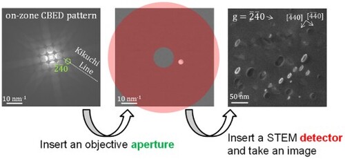
GRAPHICAL ABSTRACT
1. Introduction
Transmission electron microscopy (TEM) has been a unique tool for selective imaging of nanometer-sized dislocation loops by taking advantages of diffraction contrast [Citation1]. The ways to obtain diffraction contrast can be classified in four ways: on-axis, off-axis, on-zone and off-zone. and schematically show the classification examples for conventional TEM (CTEM) and scanning TEM (STEM) modes, respectively. On-axis or off-axis is an imaging condition in which the symmetrical axis of the imaging beam(s) (red dashed line in and ) distribution is or is not overlapped with the optical axis (orange dashed line in and ) of the TEM. On-zone or off-zone is an illumination condition in which a zone axis (purple solid line in and ) of the TEM specimen is or is not along the symmetrical axis of the incident electron beam (green broad solid line in and ) distribution. Generally, the on-axis and on-zone condition causes low selectivity in dislocation-loop imaging in both CTEM (a) and STEM modes (a and c). Despite an abundance of imaging methods, TEM operators still need advanced skills and experience to reliably achieve an appropriate imaging. This is because the diffraction contrast is sometimes strongly affected by the TEM specimen shape itself, such as a bent specimen, which produces equal-inclination fringes or a specimen having a thickness change, which produces equal-thickness fringes. These fringes can cause significant contrast relative to the matrix, requiring the TEM operator to selectively highlight the dislocation loops of interest. It is conventionally believed that the only way to highlight a selected dislocation loop is to conduct accurate tilting of the TEM specimen from the on-zone condition (e.g. a) to meet specific excitation conditions (e.g. b and c), such as using the weak-beam (WB) method [Citation2,Citation3]. Such accurate tilting can only be reliably performed by highly skilled TEM operators, making it difficult to accumulate the large amount of imaging data needed to systematically investigate the effects of dislocation loops thought to produce material property changes, such as irradiation embrittlement of reactor pressure-vessel steel [Citation4,Citation5].
Figure 1. Schematic examples of classification in CTEM mode, where cyan, magenta, and green line below the specimen shows diffraction wave of cyan plane, diffraction wave of magenta plane and transmitted wave, respectively. (a) On-axis and on-zone BF-CTEM. (b) On-axis and off-zone BF-CTEM. (c) On-axis and off-zone DF-CTEM. (d) Off-axis and on-zone DF-CTEM. (e) Off-axis and off-zone DF-CTEM.
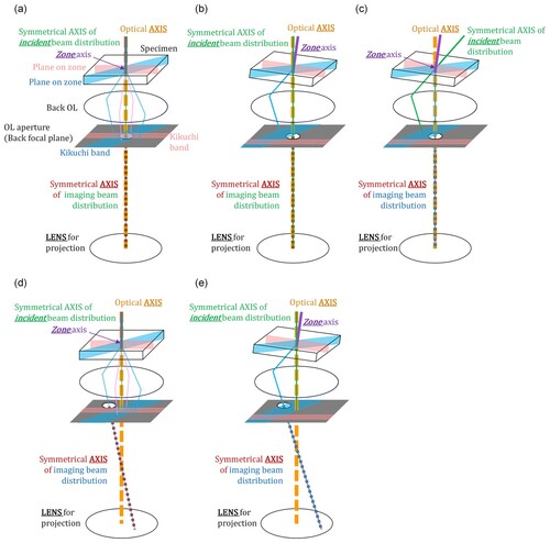
Figure 2. Schematic examples of classification in STEM mode, where cyan, magenta, and green line below the specimen shows diffraction wave of cyan plane, diffraction wave of magenta plane and transmitted wave, respectively. (a) On-axis and on-zone BF-STEM. (b) On-axis and off-zone BF-STEM. (c) On-axis and on-zone DF-STEM. (d) Off-axis and on-zone DF-STEM. (e) Off-axis and off-zone DF-STEM.
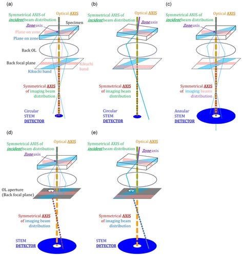
Until recently, TEM operators exclusively used a parallel electron beam to obtain a projection image of the dislocation loops in the CTEM mode [Citation6]. The diffraction contrast obtained by the parallel beam is sensitive to the specimen bending and thickness changes. The spatial resolution of the projection image is lost in the off-axis condition (d and e) because the imaging beam does not reach the projection lens centre, where the image is sharply magnified. This is why dark-field (DF) imaging in the off-axis and on-zone condition (d) is not widely employed for selective imaging of dislocation loops despite its excellent useability of just selecting a diffraction spot of interest using an objective lens (OL) aperture. However, recent development and investigation of the STEM mode [Citation7,Citation8], which uses a sub-nanometre-sized convergent beam to obtain a scanned image without the projection-lens system, has expanded the application area of the on-zone imaging (e.g. a and c) [Citation9–11] as well as the off-axis and off-zone imaging (e) [Citation12–15]. Zhu et al. revealed that the fringes are suppressed when both the convergence angle and detection angle are greater than or equal to a few milliradians [Citation16]. Yoshida et al. reported that small dislocation loops (diameter 1–3 nm) can be sharply imaged with WB-STEM [Citation17], which is an off-axis and off-zone DF-STEM (e).
Despite the recent remarkable advances in the STEM mode, including 4D-STEM [Citation10], application of a physical aperture to STEM imaging has been limited to off-axis and off-zone conditions (e) [Citation14,Citation16–21] and the on-axis and on-zone conditions [Citation22] (a). To the authors’ knowledge, there has been no report on successful imaging of dislocation loops by the off-axis and on-zone DF-STEM (d) despite its ease of operation. In this work, we propose diffraction-selected on-zone STEM (DsoZ-STEM) as one of the easiest ways for selective DF imaging of dislocation loops by off-axis and on-zone DF-STEM. The main object of this work therefore is to demonstrate that DsoZ-STEM can simplify the selective imaging of dislocation loops with high accuracy in determination of their character and number.
2. Materials and methods
2.1. Specimen preparation
A TEM specimen was made from a single-crystal aluminum of >99.99% purity (MTI Corporation) by electropolishing using TENUPOL (Struers S.A.S.). The electropolished specimen was irradiated with 100 eV argon ions and 300 keV electrons at 303 K using a broad-ion-beam milling machine (PIPS II (Gatan, Inc.)) and a transmission electron microscope (JEM-ARM300F (JEOL Ltd.)), respectively. It has been reported that interstitial dislocation loops are formed in pure aluminum during 150 keV electron-beam irradiation after ion-beam irradiation with 12 keV He+ or 15 keV H+ ions [Citation23].
2.2. Experimental setup
All STEM imaging experiments were conducted on a JEM-ARM300F (JEOL Ltd.) equipped with a CMOS camera OneView 1095 (Gatan, Inc.), an annular DF (ADF) and a circular bright-field (BF) STEM detector. On-zone [001] STEM images (20482048 pixels) and a convergent-beam electron diffraction (CBED) pattern (4096
4096 pixels) were taken with optical settings as follows:
condenser lens (CL) aperture diameter: 10 μm,
Spherical aberration corrector: on at illumination system,
OL aperture diameter: 20 μm,
camera length: 40 cm.
The dwell time of the STEM image and exposure time of the CBED pattern were 38.9 μs (163 s/image) and 2 s (2 s/pattern), respectively. All the optical elements used in this study were commercial products without any specialties.
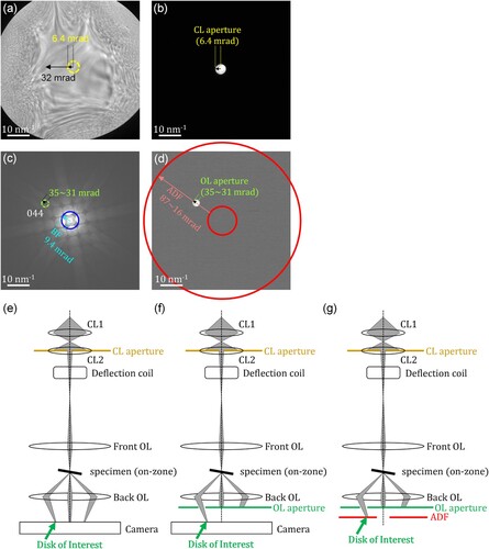
shows an experimental setup for DsoZ-STEM imaging. Although the spherical aberration-corrected electron beam gave a ronchigram pattern with an area of largely uniform electron intensity (a), only a small area was selected by the condenser aperture (b) to obtain a CBED pattern without overlap among disks (c and e). Since the used convergence angle is small (semi-angle: 6.4 mrad), the spherical aberration corrector is not necessary for DsoZ-STEM. A diffraction disk of interest was selected using the OL aperture (d and f). This operation corresponds to selecting a reflection vector g originated from a Bragg diffraction [Citation19,Citation20]. Then, the ADF-STEM detector was inserted to detect the selected diffraction disk (g). As schematically shown in e and f, DsoZ-STEM imaging can be conducted without any special optical elements. For comparison, a BF-STEM image was taken with the BF-STEM detector (c). The imaging area was approximately 155 nm in thickness, determined by a conventional log-ratio technique [Citation24], for which the inelastic mean free path was experimentally determined as 245 nm.
Figure 3. Experimental setup. (a) Ronchigram example taken from amorphous region in TEM specimen of the single crystalline aluminum. The yellow dashed circle shows position example and size of the condenser aperture with a diameter of 10 μm. (b) The result of the condenser aperture insertion. (c) CBED pattern example taken from crystalline region in TEM specimen of the
single crystalline aluminum along the
zone axis. The green dashed circle and blue solid circle shows position example and size of the OL aperture with a diameter of 20 μm and the BF-STEM detector, respectively. (d) The result of the OL aperture insertion to the centre of 044 disk. The red solid circle shows position example and size of the ADF-STEM detector. (e) Schematic of setup for (c). (f) Schematic of setup for (d). (f) Schematic of setup for DsoZ-STEM.
3. Results and discussion
3.1. Applicability of invisibility criterion
shows a result of an applicability test using the g b invisibility criterion. The BF-STEM image (b) showed the existence of a dislocation line and many elliptical dislocation loops. Since the long axis of the elliptical dislocation loops seems to be parallel to the [] or [
] direction (a), based on a morphological method to determine the loop type proposed by Yao et al. [Citation6] and Xiu et al. [Citation25], it was expected that the dislocation loops exclusively have a Burgers vector b of 1/3
. Details of dislocation loops investigated in this study are listed in . c and d are DsoZ-STEM images with a diffraction disk of
and
(a), respectively. Note that the dislocation loops with their long axis parallel to the [
] and [
] direction are invisible in c and d, respectively. This means that the g·b invisibility criterion can be applied to DsoZ-STEM and will be helpful to resolve and identify overlapping dislocation loops. Under the off-axis and on-zone DF condition, the selected g has an excitation error sg with the magnitude which increases with increase in the distance from the transmitted disk. We assume that the sg gave the DsoZ-STEM image a contrast which is similar to the WB-method.
Figure 4. Applicability test of g b invisibility criterion. (a) On zone [001] CBED pattern with the positions and size of inner edge of the ADF-STEM detector (red solid circle), outer edge of the BF-STEM detector (blue solid circle) and the OL aperture (green dashed circle). (b) BF-STEM image. (c) DsoZ-STEM image with [001] zone axis and diffraction disk. (d) DsoZ-STEM image with [001] zone axis and
diffraction disk. The small dislocation marked by orange solid ellipse appears to have a long axis parallel to [
] direction in (b) but is visible in (d) not (c).
![Figure 4. Applicability test of g b invisibility criterion. (a) On zone [001] CBED pattern with the positions and size of inner edge of the ADF-STEM detector (red solid circle), outer edge of the BF-STEM detector (blue solid circle) and the OL aperture (green dashed circle). (b) BF-STEM image. (c) DsoZ-STEM image with [001] zone axis and 4¯40 diffraction disk. (d) DsoZ-STEM image with [001] zone axis and 4¯4¯0 diffraction disk. The small dislocation marked by orange solid ellipse appears to have a long axis parallel to [4¯4¯0] direction in (b) but is visible in (d) not (c).](/cms/asset/bd68f238-f35b-43cb-9e44-d7a028b60b0c/tphl_a_2321134_f0004_oc.jpg)
Table 1. Details of dislocation loops investigated in this study.
The small dislocation marked in b appears to have a long axis parallel to the [] direction but is visible in the marked region of d. In other words, the marked dislocation loop is visually of 1/3
or 1/3
type, but in reality is appropriately classified as 1/3
or 1/3
type (). This is because the dislocation is too small (<2 nm in short-axis length) to correctly identify the shape [Citation21], showing a limitation of the morphological method, which uses the on-zone and on-axis BF image. However, DF based approaches such as DsoZ-STEM can be applied to the characterization of dislocation loops with such a small size.
3.2. Highlighting effect by a Kikuchi line
shows an effect of a Kikuchi line in DsoZ-STEM. In DsoZ-STEM images with a diffraction disk of (b) and
(c), dislocation loops with a long axis parallel to [
] had higher brightness compared to those with a long axis parallel to the [
] direction. The specific dislocation loops are highlighted in b and c. We assume the highlighting effect arises from a contribution of Kikuchi diffraction by {
} planes because the Kikuchi line associated with the (
) and (
) planes, shown by solid and dashed lines in a, lie across the diffraction disk centre of
and
, respectively. For example, the contrast of the DsoZ-STEM image with a diffraction disk of
(b) would be composed of a Bragg diffraction by (
) planes and a Kikuchi diffraction by (
) planes (). Although the selected region on the diffraction disk of
(a) contained the Kikuchi line of both (
) and (
) planes (not shown in a), dislocation loops with a long axis parallel to the [
] direction were invisible in d (same as d). This indicates that the contribution of Kikuchi diffraction by the (
) and (
) planes to the visibility of the dislocation loops can be ignored in DsoZ-STEM. The brightness profile taken from selected area A, which contains both matrix and a dislocation loop with its long axis parallel to [
] direction, is shown in e. The normalized brightness value was calculated by dividing the brightness value by the minimum brightness value in the profile to assess the contrast between the matrix and the dislocation loop of each image. The contrast in g =
and g =
was higher than that in g =
by around 1.5 times. Note that the marked dislocation loop is visible in b and c but almost invisible in d. This indicates that highlighting of dislocation loops utilizing a Kikuchi line is effective also in DsoZ-STEM imaging as well as in two-beam DF imaging, where the selected hkl disk is excited by the Kikuchi line of the (
) plane (e.g. e). However, the highlighting effect by a Kikuchi line must be traded-off against spatial resolution since the incident electron beam gets broadened by inelastic scattering produced by Kikuchi diffraction. In fact, the profile of g =
, where the Kikuchi line of {
} plane is not contained has the sharpest peak in e. There is a possibility that the highlighting effect works under limited thickness ranges where inelastic scattering is sufficiently strong, but not dominant so that the electron beam does not become too broad and reduce scan resolution.
Figure 5. Highlighting of dislocation loops utilizing a Kikuchi line. (a) On zone [001] CBED pattern with the positions and size of inner edge of the ADF-STEM detector (red solid circle) and the OL aperture (green dashed circle). The white solid and dashed line shows a position of Kikuchi line of () plane and (
) plane. (b) DsoZ-STEM image with [001] zone axis and
diffraction disk containing defect Kikuchi line of (
) plane. (c) DsoZ-STEM image with [001] zone axis and
diffraction disk containing Kikuchi line of (
) plane. (d) DsoZ-STEM image with [001] zone axis and
diffraction disk. (e) Brightness profile of the selected area A (yellow solid line rectangle in (b)–(d)). The normalized brightness value was calculated by dividing the brightness value by minimum brightness value in the profile. The faint dislocation marked by orange solid line ellipse is visible in (b) and (c) but almost invisible in (d).
![Figure 5. Highlighting of dislocation loops utilizing a Kikuchi line. (a) On zone [001] CBED pattern with the positions and size of inner edge of the ADF-STEM detector (red solid circle) and the OL aperture (green dashed circle). The white solid and dashed line shows a position of Kikuchi line of (2¯20) plane and (22¯0) plane. (b) DsoZ-STEM image with [001] zone axis and 2¯4¯0 diffraction disk containing defect Kikuchi line of (2¯20) plane. (c) DsoZ-STEM image with [001] zone axis and 4¯2¯0 diffraction disk containing Kikuchi line of (22¯0) plane. (d) DsoZ-STEM image with [001] zone axis and 4¯4¯0 diffraction disk. (e) Brightness profile of the selected area A (yellow solid line rectangle in (b)–(d)). The normalized brightness value was calculated by dividing the brightness value by minimum brightness value in the profile. The faint dislocation marked by orange solid line ellipse is visible in (b) and (c) but almost invisible in (d).](/cms/asset/1b3c09ee-814f-4150-add4-28f2594ba1f6/tphl_a_2321134_f0005_oc.jpg)
3.3. Applicability of left-side and right-side experiment
shows the result of a left-side and right-side experiment using a dislocation line. The dislocation line was almost parallel to the [] direction and had high brightness in DsoZ-STEM images with a diffraction disk of
(b) and
(c). This is a result of highlighting effect of Kikuchi diffraction by (
) and (
) plane, respectively. The selected area B contains not only the dislocation line but also a dislocation loop as a positional landmark. The brightness profile taken from area B is shown in e, where a reference position of the dislocation loop and the dislocation line are given by the BF profile calculated from the BF-STEM image (d). The normalized brightness value was calculated by dividing the brightness value by maximum brightness value in the profile to compare peak positions between g =
and
. This clearly shows a positional shift in the dislocation line of g =
(left-side) and
(right-side) from the real position, in good agreement with the typical visibility change of conventional DF images with a specific pair of ±g. Thus, determination of the sign of the Burgers vector can be conducted even using DsoZ-STEM images.
Figure 6. Visibility confirmation of dislocation line using a specific pair of g. (a) On zone [001] CBED pattern with the positions and size of inner edge of the ADF-STEM detector (red solid circle), outer edge of the BF-STEM detector (blue solid circle) and the OL aperture (green dashed circle). (b) DsoZ-STEM image with [001] zone axis and
diffraction disk. (c) DsoZ-STEM image with [001] zone axis and
diffraction disk. (d) BF-STEM image. (e) Brightness profile of the selected area B (yellow solid line rectangle in (b)–(d)). The normalized brightness value was calculated by dividing the brightness value by maximum brightness value in each profile.
![Figure 6. Visibility confirmation of dislocation line using a specific pair of ±g. (a) On zone [001] CBED pattern with the positions and size of inner edge of the ADF-STEM detector (red solid circle), outer edge of the BF-STEM detector (blue solid circle) and the OL aperture (green dashed circle). (b) DsoZ-STEM image with [001] zone axis and 42¯0 diffraction disk. (c) DsoZ-STEM image with [001] zone axis and 4¯20 diffraction disk. (d) BF-STEM image. (e) Brightness profile of the selected area B (yellow solid line rectangle in (b)–(d)). The normalized brightness value was calculated by dividing the brightness value by maximum brightness value in each profile.](/cms/asset/ed344ac7-bd42-44cd-a4fb-8c8ca859e765/tphl_a_2321134_f0006_oc.jpg)
3.4. Applicability of in-side and out-side experiment
shows the result of in-side and out-side experiment using dislocation loops. All of the dislocation loops with a long axis parallel to [] that have high brightness in the DsoZ-STEM image with a diffraction disk of
(b) had low brightness in the DsoZ-STEM image with a diffraction disk of
(c). The selected area C contains a dislocation loop with long axis parallel to [
] direction. The brightness profile taken from the area C is shown in (e), where a reference position of the dislocation loop edges is given by the BF profile calculated from the BF-STEM image (d). This clearly shows a positional shift in the dislocation loop edge of g =
(out-side) and
(in-side), respectively, in good agreement with the typical visibility change of a dislocation loop in DF images with a specific pair of
g. Note that the brightness peak showing in-side of the dislocation loop (g =
) is higher than that showing out-side of the dislocation loop (g =
) by around 1.5 times in e. Such a tendency was confirmed in relatively large dislocation loops in b and c and b and c. Therefore, DsoZ-STEM is expected to simplify the distinction of dislocation loops with apparently the same long axis direction but different b, which cannot be conducted by the g·b invisibility criterion ().
Figure 7. Visibility confirmation of dislocation loop using a specific pair of g. (a) On zone [001] CBED pattern with the positions and size of inner edge of the ADF-STEM detector (red solid circle), outer edge of the BF-STEM detector (blue solid circle) and the OL aperture (green dashed circle). (b) DsoZ-STEM image with [001] zone axis and
diffraction disk. (c) DsoZ-STEM image with [001] zone axis and
diffraction disk. (d) BF-STEM image. (e) Brightness profile of the selected area C (yellow solid line rectangle in (b)–(d)).
![Figure 7. Visibility confirmation of dislocation loop using a specific pair of ±g. (a) On zone [001] CBED pattern with the positions and size of inner edge of the ADF-STEM detector (red solid circle), outer edge of the BF-STEM detector (blue solid circle) and the OL aperture (green dashed circle). (b) DsoZ-STEM image with [001] zone axis and 420 diffraction disk. (c) DsoZ-STEM image with [001] zone axis and 4¯2¯0 diffraction disk. (d) BF-STEM image. (e) Brightness profile of the selected area C (yellow solid line rectangle in (b)–(d)).](/cms/asset/2f84501e-37bf-450d-b906-850031f7f794/tphl_a_2321134_f0007_oc.jpg)
4. Conclusions
In this work, we investigated the applicability of DsoZ-STEM to selective imaging of dislocation loops in terms of their character and size in a single crystal aluminum (purity: >99.99%) irradiated by Ar ions and an electron beam at room temperature. It was possible to conduct DsoZ-STEM imaging using only optical elements available in conventional commercial products. TEM operators just select a diffraction disk of interest using an OL aperture from an on-zone CBED pattern obtained by an incident electron beam with small convergent angle (several mrads in semi-angle). DsoZ-STEM is applicable to selective DF imaging of dislocation loops with a short axis length of <2 nm, which is out of the application range of the morphological method to characterize dislocation loops using an on-zone BF-STEM image. DsoZ-STEM imaging obeys the g b invisibility criterion. This is particularly powerful in resolving and identifying overlapping dislocation loops. It is shown that a Kikuchi line enhances the contrast among the dislocation loops and the matrix of an DsoZ-STEM image. Since a specific diffraction disk is not strongly excited at on-zone condition, such a contrast enhancement could be helpful to avoid miscounting dislocation loops. The DsoZ-STEM image also showed good agreement with a typical visibility change of dislocation lines and loops in conventional DF images with
g. In addition, dislocation loops always showed much higher brightness in the in-side compared to the out-side in DsoZ-STEM images. This will simplify the distinction of dislocation loops with apparently the same long axis direction but different b.
This work shows that DsoZ-STEM simplifies the selective imaging of dislocation loops with high accuracy in determination of their character and number. In this way, TEM operators can appropriately conduct DF imaging of dislocation loops of interest without accurate tilting operations of the TEM specimen and installation of specific optical elements. DsoZ-STEM, therefore, will greatly contribute to accumulation of imaging data in multi-institutional collaboration research for systematic investigation of the effect of dislocation loop on material properties.
Acknowledgements
The authors thank Mr Sho Tamaru and Mr Ryota Kinoshita of Kobe Material Testing Laboratory Co., Ltd for technical support of the electropolishing process for TEM specimen preparation.
Disclosure statement
No potential conflict of interest was reported by the author(s).
Additional information
Funding
Notes on contributors
Masaya Kozuka
Masaya Kozuka is a research scientist of microscopy (especially APT and TEM) and neutron irradiation embrittlement at Central Research Institute of Electric Power Industry (CRIEPI). His work focuses recently on the relationship between dislocation loop formation and embrittlement of the reactor pressure vessel steels. His favourite is running along the coast near his home.
Yuichi Miyahara
Yuichi Miyahara is a research scientist of microstructural analysis (EBSD, TEM, APT) and characterization of environmental degradation of structural materials (Stress Corrosion Cracking, Irradiation hardening and embrittlement) at CRIEPI. His work focuses recently on microstructural evolution of irradiated stainless steels and reactor pressure vessel steels
References
- P. Hirsch, D. Cockayne, J. Spence, and M. Whelan, 50 years of TEM of dislocations: Past, present and future, Phil. Mag 86 (2006), pp. 4519–4528.
- D.J.H. Cockayne, I.L.F. Ray, and M.J. Whelan, Investigations of dislocation strain fields using weak beams, Phil. Mag 20 (1969), pp. 1265–1270.
- S.J. Zinkle, and B.N. Singh, Microstructure of neutron-irradiated iron before and after tensile deformation, J. Nucl. Mater 351 (2006), pp. 269–284.
- H. Watanabe, S. Masaki, S. Masubuchi, N. Yoshida, and K. Dohi, Effects of Mn addition on dislocation loop formation in A533B and model alloys, J. Nucl. Mater 439 (2013), pp. 268–275.
- T. Fujita, J. Hirabayashi, Y. Katayama, F. Kano, and H. Watanabe, Contribution of dislocation loop to radiation-hardening of RPV steels studied by STEM/EDS with surveillance test pieces, J. Nucl. Mater 572 (2022), pp. 154055.
- B. Yao, D.J. Edwards, and R.J. Kurtz, TEM characterization of dislocation loops in irradiated bcc Fe-based steels, J. Nucl. Mater 434 (2013), pp. 402–410.
- C.J. Humphreys, Fundamental concepts of stem imaging. Ultramicroscopy 7 (1981), pp. 7–12.
- P.J. Phillips, Diffraction contrast STEM of dislocations: Imaging and simulations, M.C. Brandes, M.J. Mills and M. De Graef, eds., Ultramicroscopy 111 (2011), pp 1483–1487.
- C.M. Parish, K.G. Field, A.G. Certain, and J.P. Wharry, Application of STEM characterization for investigating radiation effects in BCC Fe-based alloys, J. Mater. Res 30 (2015), pp. 1275–1289.
- C. Gammer, V.B. Ozdol, C.H. Liebscher, and A.M. Minor, Diffraction contrast imaging using virtual apertures, Ultramicroscopy 155 (2015), pp. 1–10.
- K.G. Field, S.A. Briggs, K. Sridharan, Y. Yamamoto, and R.H. Howard, Dislocation loop formation in model FeCrAl alloys after neutron irradiation below 1 dpa, J. Nucl. Mater 495 (2017), pp. 20–26.
- M. Tanaka, K. Higashida, K. Kaneko, S. Hata, and M. Mitsuhara, Crack tip dislocations revealed by electron tomography in silicon single crystal, Scripta Mater 59 (2008), pp. 901–904.
- H. Iwata, and H. Saka, Resolving individual Shockley partials of a dissociated dislocation by STEM, Phil. Mag. Lett 97 (2017), pp. 74–81.
- Y. Du, K. Yoshida, Y. Shimada, T. Toyama, K. Inoue, K. Arakawa, T. Suzudo, K.J. Milan, R. Gerard, S. Ohnuki, and Y. Nagai, In-situ WB-STEM observation of dislocation loop behavior in reactor pressure vessel steel during post-irradiation annealing, Materialia 12 (2020), pp. 100778.
- A. Mussi, A. Addad, and F. Onimus, Dislocation electron tomography: A technique to characterize the dislocation microstructure evolution in zirconium alloys under irradiation, Acta Mater. 213 (2021), pp. 116964.
- Y. Zhu, C. Ophus, M.B. Toloczko, and D.J. Edwards, Towards bend-contour-free dislocation imaging via diffraction contrast STEM, Ultramicroscopy 193 (2018), pp. 12–23.
- K. Yoshida, M. Shimodaira, T. Toyama, Y. Shimizu, K. Inoue, T. Yoshiie, K.J. Milan, R. Gerard, and Y. Nagai, Weak-beam scanning transmission electron microscopy for quantitative dislocation density measurement in steels, Microscopy. 66 (2017), pp. 120–130.
- P.J. Phillips, M.J. Mills, and M. De Graef, Systematic row and zone axis STEM defect image simulations, Phil. Mag 91 (2011), pp. 2081–2101.
- J. Miao, S. Singh, J. Tessmer, M. Shih, M. Ghazisaeidi, M. DeGraef, and M.J. Mills, Dislocation characterization using weak beam dark field STEM imaging, Microsc. Microanal 24(Suppl. 1) (2018), pp. 2202–2203.
- J. Miao, High resolution imaging of dislocations using weak beam dark field STEM, Microsc. Microanal 26(Suppl. 2) (2020), pp. 1220–1222.
- J. Miao, C. Slone, S. Dasari, M. Ghazisaeidi, R. Banerjee, E.P. George, and M.J. Mills, Ordering effects on deformation substructures and strain hardening behavior of a CrCoNi based medium entropy alloy, Acta Mater. 210 (2021), pp. 116829.
- E. Oveisi, A. Letouzey, D.T.L. Alexander, Q. Jeangros, R. Schäublin, G. Lucas, P. Fua, and C. Hébert, Tilt-less 3-D electron imaging and reconstruction of complex curvilinear structures, Sci. Rep 7 (2017), pp. 10630.
- K. Ono, H. Ogawa, S. Furuno, T. Kino, N. Kamigaki, K. Hojou, Shibatani, Y. Kagcyama, K. Mizuno, and K. Ito, Formation of interstitial loops on transmutation products in aluminum, J. Nucl. Mater 191–194 (1992), pp. 1209–1213.
- T. Malis, S.C. Cheng, and R.F. Egerton, EELS log-ratio technique for specimen-thickness measurement in the TEM, J. Electron Microsc. Tech 8 (1988), pp. 193–200.
- P. Xiu, H. Bei, Y. Zhang, L. Wang, and K.G. Field, STEM characterization of dislocation loops in irradiated FCC alloys, J. Nucl. Mater 544 (2021), pp. 152658.