Abstract
This paper focuses on the conduction regime of a monolayer single-carrier organic light-emitting diodes (OLEDs). First, a model that has no pre-assumption regarding the conduction regime of OLED, and therefore, is accurate in both the conduction regimes of injection-limited current (ILC) and space charge-limited current (SCLC), is introduced. The model is verified against experimental data, and it is demonstrated that it is accurate in a wide range of bias voltages and barrier heights. Subsequently, a quantitative index for the conduction regime is introduced for the first time, which is called the injection/transport index (ITI). All the important factors regarding the conduction regime, such as bias voltage, barrier height, carrier mobility, device length, and temperature are included in the analytical formula introduced for ITI. The ITI value versus bias voltage, barrier height, and carrier mobility are studied in the paper in detail, and it is demonstrated that positive ITIs are related to the SCLC regimes, while negative ITIs are related to the ILC regimes. Furthermore, the method of using ITI in two-carrier and multi-layers devices is also discussed.
1. Introduction
Organic light-emitting diodes (OLEDs), after the initial introduction by Tang and Vanslyke [Citation1], have been developed considerably in recent years and used in many applications, including large displays and general luminescence [Citation2–4]. This progress has been achieved through extensive experimental and theoretical researches. In 1997, Davids et al. [Citation5] did pioneering work on the I–V characteristic in the form of a numerical solution for the OLED equations. Later, theoretical work focused on the electric conduction classification, arguing that it is either in a contact-limited regime (called the injection-limited current, ILC) or in a bulk-limited regime (called the space charge-limited current, SCLC). When the potential barrier height at the metal/organic interface is high enough, the ILC regime dominates, resulting in an exponential –
characteristic. When the bulk carrier mobility is low enough (in low potential barrier height cases), the SCLC regime dominates, resulting in a square power law for the I–V characteristic [Citation5–7]. The square power law was introduced in 1940, and was called the Mott–Gurney formula [Citation8].
These notions are still acceptable and form the dominated language in current discussions [Citation9,Citation10]. However, recently, some supplementary sentences have been added, which state that besides the mobility and barrier height, some other parameters, such as the amount of the applied bias, active layer thickness, temperature, doping, and time should also be considered in determining the conduction regime [Citation11–14].
Nevertheless, till date, most discussions have been qualitative, and a comprehensive calculation that can incorporate both ILC/SCLC regimes and result in a quantitative index has not yet been introduced. This paper introduces such a comprehensive formulation and a clear numerical index for the conduction regime in OLEDs.
After this introduction, in Section 2, we have explained the theory and the new quantitative index, termed as the injection/transport index (ITI), and verified it against the experimental data. In Section 3, we have discussed the conduction mechanism versus bias, barrier height, and carrier mobility quantitatively using the ITI. Finally, in Section 4, we have drawn the conclusions.
2. Theory
The conduction problem in OLED can be divided into two topics. The carrier injection from contact to organic material and the carrier transport through the organic material itself. Each of these two jobs can be completed using certain different mechanisms.
Regarding to the carrier transport inside the organic material, we have [Citation15]
By considering the balance condition, the thermionic current can be re-written as
The ITI can be written as
Fig. 1. Electrical field (dot signs) and carrier density (O signs) versus position for a positive value and a negative value of ITI. All curves were calculated using the constant current density criterion (J=10 A/m2).
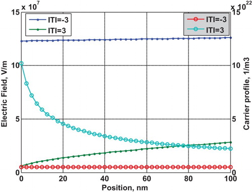
In the first case, E(0) is high and is low, which corresponds to negative ITI values. The electric field across the device is almost constant, while the carrier density is relatively low and space charges do not play a significant role. The case will occur when the barrier height is high; therefore, fewer carriers are injected into the device. In this case, one may easily take E(0) equal to V/L, and then calculate the current from Equations (9) and (10). This is the so-called ILC.
In the second limit, E(0) is low and is high which corresponds to positive ITI values. The space charge is high and plays an important role. The case occurs when the barrier height is low and injects huge carriers into the bulk. This limit is the so-called SCLC.
From Equation (16), we will have the following equation in the limit of positive ITI:
Fig. 2. The calculated I–V curves in a log–log scale for four different values of barrier heights, ϕ0, is equal to 0.1, 0.3, 0.5, and 0.7 eV. Each curve has three sections corresponding to thermionic, tunneling, and SCLC. These three regions are distinguished by three tangent numbered lines on the ϕ0=0.5 eV curve (numbers 1, 2, and 3 correspond to thermionic, tunneling, and SCLC). Also shown in the figure is the SCLC equation (Mott–Gurney equation). We can see that all curves go to SCLC equation in high biases. Other parameters in this simulation were μ0=2×10⁻¹⁰m2/V S, γ=0, and L=100 nm.
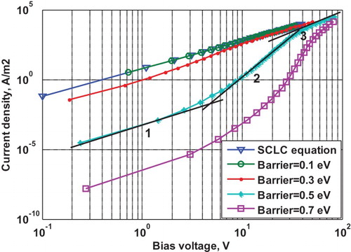
To check the validity of the model, we compared its result with three different experimental data corresponding to three different structures. The structures were ITO/α-NPD/Ag [Citation18], ITO/TPD/Al [Citation19], and ITO/m-MTDATA/Ag [Citation20], which had three different active layer thicknesses of 176, 120, and 850 nm, respectively, and shows the results. It can be observed that there is a very acceptable match for all the three experimental data in about 12 decades of current densities and 3 decades of bias voltages. On comparing with the results presented in , it can be argued that in the first experiment [Citation18], the conduction regime is totally ILC, which in low bias, is dominated by thermionic, and in high bias, is dominated by tunneling. In the second experiment [Citation19], it can be observed that in low bias, the conduction regime is ILC (by tunneling mechanism) and in high bias, it is SCLC. Furthermore, in the third experiment [Citation20], all the three above-mentioned regions are clearly distinguishable.
Fig. 3. Results of the model (solid curves) in comparison with three different sets of experimental data (the signs) taken from [Citation18–20]. The parameters with regard to the first experiment (taken from [Citation18]) were ϕ0=0.5 eV, μ0=7×10⁻¹⁰, γ=9×10⁻⁴, α=5×10⁻⁴, β=1.3×10⁻², L=176 nm; with regard to the second experiment (taken from [Citation19]) were ϕ0=0.75 eV, μ0=10−8, γ=0.1×10⁻⁴, α=70 β=3.42×10⁻², L=120 nm; and with regard to the third experiment (taken from [Citation20]) were ϕ0=0.6 eV, μ0=6×10⁻¹⁰, γ=3×10⁻⁴, α=4, β=2.4×10⁻², L=850 nm. It can be seen that there is a very acceptable agreement between the model and different experiments in very large ranges of biases and current densities.
![Fig. 3. Results of the model (solid curves) in comparison with three different sets of experimental data (the signs) taken from [Citation18–20]. The parameters with regard to the first experiment (taken from [Citation18]) were ϕ0=0.5 eV, μ0=7×10⁻¹⁰, γ=9×10⁻⁴, α=5×10⁻⁴, β=1.3×10⁻², L=176 nm; with regard to the second experiment (taken from [Citation19]) were ϕ0=0.75 eV, μ0=10−8, γ=0.1×10⁻⁴, α=70 β=3.42×10⁻², L=120 nm; and with regard to the third experiment (taken from [Citation20]) were ϕ0=0.6 eV, μ0=6×10⁻¹⁰, γ=3×10⁻⁴, α=4, β=2.4×10⁻², L=850 nm. It can be seen that there is a very acceptable agreement between the model and different experiments in very large ranges of biases and current densities.](/cms/asset/f118eda1-fad0-4f8d-b944-22537f78f29b/tjos_a_771505_f0003_c.jpg)
3. Quantitative study of transport regime using ITI
By using the new single index given in Equation (17), one can easily determine the conduction regime in OLED in all cases quantitatively, because Equation (17) includes all the main factors, such as barrier height, bias value, carrier mobility, and temperature. In the following, we will examine the first three factors in more detail.
3.1 Applied bias
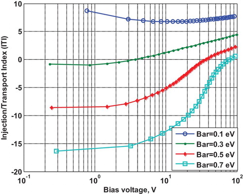
The conduction regime will change in a given device when the bias voltage changes. shows the ITI versus bias voltage for different barrier heights (all parameters and ranges are same as those given in ). In the figure, if one wants to have a qualitative description of the conduction regime using the above-mentioned quantitative index, then the ITI=0 criterion can be considered as a good indicator, consequently, the positive ITI shows SCLC regime and the negative ITI shows ILC regime. From the figure, it can be concluded that by using the above-mentioned criterion, the conduction regime is most likely to be ILC in high barrier heights, while it is always SCLC in low-barrier heights. Furthermore, in moderate barrier heights, it is ILC in low bias range and SCLC in high bias. All these results are in good agreement with the previously published qualitative results [Citation21].
Fig. 4. The ITI versus applied bias for four different values of barrier height. The barrier heights, bias range, and other parameters are the same as those given in .
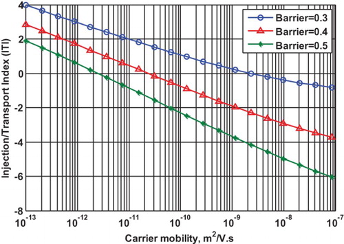
3.2 The barrier height
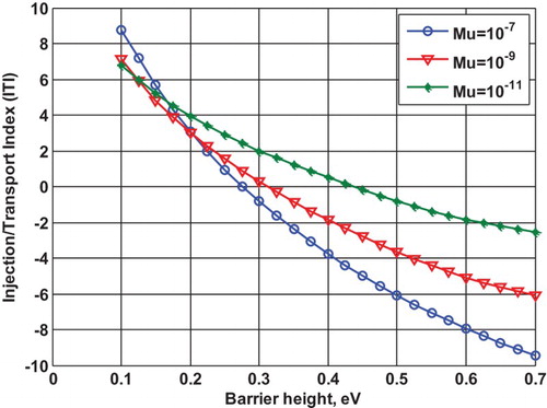
As mentioned before, in the devices with low injection barrier, the conduction regime is SCLC, and in the devices with high barrier height, it is ILC. However, we know that by increasing the barrier height, the current density decreases, and hence, we must work in higher bias voltages to have sufficient current density, and therefore, sufficient light. Hence, for a quantitative judgment of the conduction regime between the structures with different barrier heights, to prevent confusion with the above-mentioned bias effect, it is necessary to have a clear criterion for the device bias. Otherwise, the comparisons will not be meaningful. To this end, we have introduced constant power dissipation criterion, which is a good measure because power dissipation and heat is often the main limitation of a device. The results are presented in . According to the figure, for the carrier mobility equal to 10−9 m2/VS, the ITI for barriers higher than 0.32 eV is negative, i.e. the conduction regime is ILC, and for barrier below 0.32 eV, it is positive, i.e. the conduction regime is SCLC (for 1000-W/m2 power density criterion). By increasing the mobility, the boundary value shifts toward lower barrier heights and vice versa. It can be observed that the ITI confirms the previous qualitative results [Citation5,Citation6,Citation22]: at low barrier height, the conduction regime is SCLC and at high barrier height, it is ILC. However, the new results are quantitative, have a firm base, and show more details.
Fig. 5. The ITI versus barrier height for three different values of mobility in 1000-W/m2 constant power dissipation. It can be observed that by decreasing the mobility, the threshold value of barrier height for negative ITI (going to ILC limit) is increased. Other parameters used in this simulation are γ=0 and L=100 nm.
3.3 Carrier mobility
The influence of carrier mobility on the ITI has been studied under the same assumption of constant power dissipation (Section 3.2), and the results are shown in . According to the figure, for a barrier height equal to 0.4 eV, the conduction regime for mobilities higher than m2/VS is ILC (ITIs < 0), and that for mobilities lower than
m2/VS is SCLC (ITI > 0). By decreasing the barrier height, the boundary value shifts toward higher values of mobilities. It can again be seen that the ITI confirms the previous qualitative results [Citation23]: at low mobilities, the conduction regime is SCLC, and at high mobilities, it is ILC.
Fig. 6. The ITI versus carrier mobility for three different values of barrier heights in 1000-W/m2 constant power dissipation. It can be seen that by decreasing the barrier height, the threshold value of carrier mobility for negative ITI (going to ILC limit) is increased. Other parameters used in this simulation are the same as .
3.4 Application of ITI
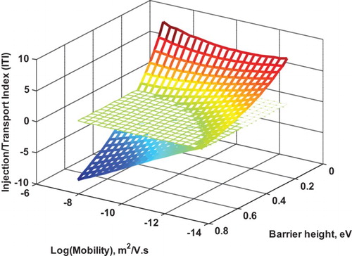
shows combination of the last two figures in a three-dimensional (3D) graph. This figure shows the ITI for a constant power dissipation (1000 W/m2) versus barrier height and mobility. Also, the ITI=0 plane, as explained before, distinguishing between ILC (bottom segment) and SCLC regions (top segment) is also presented in the figure.
Fig. 7. A 3D plot of ITI versus mobility and barrier height in 1000-W/m2 constant power dissipation. Also shown in the figure is the ITI=0 plane that distinguishes between the two limiting cases, i.e. the ILC (the regions under the plane) and the SCLC (the regions above the plane). Other parameters used in this simulation are the same as .
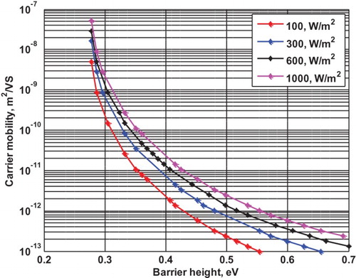
The proposed index can be used for an estimation of the conduction regime in two-carrier and/or multilayer device. shows the ITI=0 curves for some different values of power dissipation in a barrier–mobility plane (the curves obtained from a set of plots similar to that were calculated using different values of power dissipation). If we want to have an estimation regarding the conduction regime in a monolayer/two-carrier system, it will be sufficient to have an estimation regarding the current ratio of the two carriers (usually it is equal to 0.4–0.6). Subsequently, for example, if we consider this ratio as 0.6 for holes in 1000-W/m2 constant power, then we should focus on the black curve in , which is the 600-W/m2 curve, and then should consider the holes injecting barrier point and the holes mobility point on the x- and y-plane of this figure. If the referred x–y intersection lies on the right side of the black curve, then we can conclude that the holes conduction regime is ILC (see the text for details); otherwise, if the x–y intersection lies on the left side of the curve, then we can conclude that it is SCLC. Similarly, for a multilayer device, it is sufficient to have an estimation of power dissipation in the objective layer. Subsequently, by using the proper curve and the mobility and barrier height of the desired carrier in the objective layer, we can determine the estimation regarding the conduction regime from . These considerations are very helpful in optimizing a complex multilayer/two-carrier device by adjusting the conduction regime for carriers in different layers.
Fig. 8. The ITI=0 curves in a mobility/barrier-height plane for four constant power dissipations. For each curve, the points located at right correspond to ILC conduction regime and those located at left correspond to the SCLC conduction regime.
4. Conclusion
A closed-form model was proposed for I–V characteristics in single-layer, single-carrier OLEDs. It was observed that the model does not have any presumption on the injection and/or transport mechanisms, and therefore, has an extensive range of validity, which includes both ILC and SCLC regimes. The model reliability was examined by comparing its results with the experimental data in an extensive range of bias voltage and barrier heights. Subsequently, based on the introduced model, a new quantitative index was introduced for the first time, which may be used for defining the conduction regime. The index was used for a quantitative study on the conduction regime versus bias, barrier height, and mobility.
In a previous work [Citation14], we discussed that in addition to the three above-mentioned items, time variations also play an important role in determining the conduction regime when the bias voltage is time-dependent. For example, in response to an applied voltage pulse, the regime will initially be ILC, and then, slowly becomes SCLC. In future, the introduced ITI can be generalised to include such time behaviors.
References
- Tang CW, Vanslyke SA. Organic electroluminescence diode. Appl. Phys. Lett. 1987;51(913):913–915. doi: 10.1063/1.98799
- D'andrade BW, Forrest SR. White organic light emitting devices for solid state lighting. Adv. Mater. 2004;16(18):1585–1595. doi: 10.1002/adma.200400684
- Wu CC, Chen CW, Lin CL, Yang CJ. Advanced organic light-emitting devices for enhancing display performances. J. Display Technol. 2005;1(2):248–266. doi: 10.1109/JDT.2005.858942
- Reineke S, Lindner F, Schwartz G, Seidler N, Walzer K, Lüssem B, Leo K. White organic light-emitting diodes with fluorescent tube efficiency. Nature 2009;459:234–239. doi: 10.1038/nature08003
- Davids PS, Campbell IH, Smith DL. Device model for single carrier organic diodes, J. Appl. Phys. 1997;82(12):6319–6325. doi: 10.1063/1.366522
- Campbell IH, Davids PS, Smith DL, Barashkov NN, Ferraris JP. The Schottky energy barrier dependence of charge injection in organic light-emitting diodes. Appl. Phys. Lett. 1998;72(15):1863–1865. doi: 10.1063/1.121208
- Blom PWM, de Jong MJM, van Munster MG. Electric-field temperature dependence of the hole mobility in poly(p-phenylene vinylene). Phys. Rev. B. 1997;55(2):R656–R659.
- Mott NF, Gurney RW. Electronic processes in ionic crystals. Oxford: Clarendon Press; 1940. p. 168–173.
- Taylor DM. Space charges and traps in polymer electronics, IEEE Trans. Dielectr. Electr. Insul. 2006;13(5):1063–1073.
- Kumar P, Jain SC, Kumar V, Chand S, Tando RP. Effect of non-zero Schottky barrier on the J–V characteristics of organic diodes. Eur. Phys. J. E. 2009;28:361–368. doi: 10.1140/epje/i2008-10427-y
- Al Attar HA, Monkman AP. Dopant effect on the charge injection, transport, and device efficiency of an electrophosphorescent polymeric light-emitting device. Adv. Funct. Mater. 2006;16:2231–2242. doi: 10.1002/adfm.200600035
- Alvarez AL, Arredondo B, Romero B, Quintana X, Gutierrez-Llorente A, Mallavia R, Otón JM. Analytical evaluation of the ratio between injection and space-charge limited currents in single carrier organic diodes. IEEE Trans. Electron. Dev. 2008;55(2):674–680. doi: 10.1109/TED.2007.912995
- Agrawal R, Kumar P, Ghosh S, Kumar Mahapatro A. Thickness dependence of space charge limited current and injection limited current in organic molecular semiconductors. Appl. Phys. Lett. 2008;93:1–3. doi: 10.1063/1.2974084
- Sharifi MJ. Time-dependent simulation of organic light-emitting diodes. Semicond. Sci. Technol. 2009;24:085019. doi: 10.1088/0268-1242/24/8/085019
- Lupton JM, Samuel IDW. Temperature-dependent single carrier device model for polymeric light emitting diodes. J. Phys. D: Appl. Phys. 1999;32:2973–2984. doi: 10.1088/0022-3727/32/23/301
- Martin SJ, Walker AB, Campbell AJ, Bradley DDC. Electrical transport characteristics of single-layer organic devices from theory and experiment. J. Appl. Phys. 2005;98:1–8.
- Davids PS, Kogan SM, Parker ID, Smith DL. Charge injection in organic light-emitting diodes: tunneling into low mobility materials. Appl. Phys. Lett. 1996;69(15):2270–2272. doi: 10.1063/1.117530
- Garcia-Belmonte G, Bisquert J, Bueno PR, Graeff CFO, Castro FA. Kinetics of interface state-limited hole injection in naphthylphenylbiphenyl diamine (NPD) thin layers. Synth. Met. 2009;159:480–486. doi: 10.1016/j.synthmet.2008.11.004
- Minagawa M, Shinbo K, Kato K, Kaneko F. Thermal properties of conduction current and carrier behavior in an organic electroluminescent device. Electron. Commun. Jpn 2009;92(3):635–641. doi: 10.1002/ecj.10048
- Staudigel J, Stößel M, Steuber F, Simmerer J. A quantitative numerical model of multilayer vapor-deposited organic light emitting diodes. J. Appl. Phys. 1999;86(7):3895–3910. doi: 10.1063/1.371306
- Jain SC, Geens W, Mehra A, Kumar V, Aernouts T, Poortmans J, Mertens R, Willander M. Injection- and space charge limited-currents in doped conducting organic materials. J. Appl. Phys. 2001;89(7):3804–3810. doi: 10.1063/1.1352677
- Blom PWM, Vissenberg MCJM. Charge transport in poly (p-phenylene vinylene) light-emitting diodes. Mater. Sci. Eng. 2000;27:53–94. doi: 10.1016/S0927-796X(00)00009-7
- Shen Y, Klein MW, Jacobs DB, Scott JC, Malliaras GG. Mobility-dependent charge injection into an organic semiconductor. Phys. Rev. Lett. 2001;86(17):3867–3870. doi: 10.1103/PhysRevLett.86.3867