
Abstract
We report the development of an all-organic active pixel sensor (APS) composed of a poly3-hexylethiophene (P3HT) and phenyl-C61-butryic acid methyl ester (PCBM) organic photodiode (OPD) connected to two organic field effect transistors and present here a study of its electro-optical characteristics. The OPD showed dark currents of 17.5 nA cm−2 with an external quantum efficiency of 30%. Our organic transistors feature UV-curable ion gels to obtain a high-capacitance dielectric with a combination of high electronic mobility, up to 4 cm2 V−1 s−1, and extremely low operating voltage, below 2 V. The APS configuration gives an in-pixel amplification of the photodetector response, with the gain reaching 40 under a 41 mW cm−2 illumination.
1. Introduction
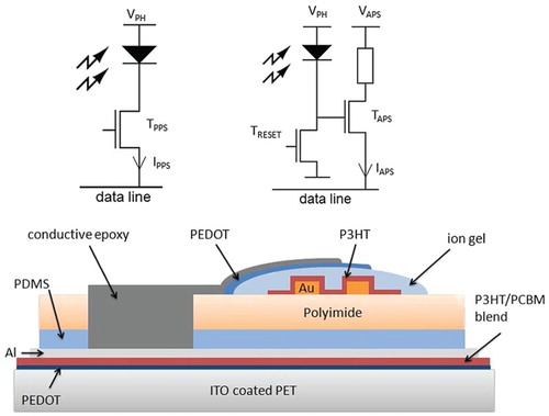
Industrial demand for flexible, low-cost, lightweight electronics has been a strong driver for the development of organic electronic devices; key applications include flexible displays,[Citation1] solar cells [Citation2] and radio frequency identification tags.[Citation3] A major advantage to organic materials is the ability to deposit them onto flexible substrates via spin coating or ink jet printing. This approach has been used to great effect in making flexible organic field effect transistors (OFET),[Citation4–6] organic photodiodes (OPD) [Citation7] and organic light-emitting diodes[Citation8]; a current focus in the field is combining these devices to make more useful ‘integrated device’ technologies. Two different photosensitive configurations have been used in the photodetection industry: the Passive Pixel Sensor (PPS) and the Active Pixel Sensor (APS). Whereas the PPS has the sensor connected via a readout transistor to the output circuitry (Figure (a)), in the APS the photodiode controls a transistor's gate voltage giving direct amplification of the input signal (Figure (b)). This direct amplification in the APS carries the advantages of better signal-to-noise ratio and enhanced dim light detection capacity,[Citation9] making them highly desirable compared to PPSs.
Figure 1. (a) PPS pixel and (b) two transistors APS layouts and (c) schematic illustration of the all-organic transistor and photosensor combination in APS architecture (only Taps is depicted).
Organic PPS arrays were developed by combining OFETs and OPDs.[Citation9,Citation10] However, one issue that stood in the way of all-organic APSs on flexible substrates is a well-known difficulty with OFETs: operating at relatively high operating voltages due to issues with the gate dielectric. As a result, many APS prototypes have kept the transistor channel inorganic in order to retain low operating voltage while moving to an organic semiconductor for the photodiode to extract the fabrication and cost benefits of organic materials however still fabricated on rigid substrates.[Citation11] Recent research on improved gate dielectrics for organic transistors, in particular the development of ion gels have led to OFETs with operating voltages [Citation4] as low as 2 V that open a path forward to all-organic APSs on flexible substrates with competitive operating voltage requirements.
In this paper we report the development of a novel APS with operating voltage as low as −1 V where all the components are organic. PPS structures were also fabricated with the same components having the same geometries for comparison. These transistors are solution processable which makes them a good candidate for low-cost fabrication. The OPD is made on a flexible polyethylene terephthalate (PET) and a thin layer of polydimethylsiloxane (PDMS) deposited on top of the OPD bonds a polyimide (PI) substrate holding the consecutively fabricated organic transistors (Figure (c)). Our photosensors show excellent performance characteristics including dark currents of 17.5 nA cm−2 with an external quantum efficiency (EQE) of 30%. APSs using inorganic transistors and photosensors have vastly been studied.[Citation12,Citation13] A hybrid architecture with inorganic transistors and organic photosensors has been developed by Tedde et al.[Citation11] This device will be compared to our APS in the electro-optical characterisation section.
2. Experimental details
A schematic of our active pixel photosensor architecture is shown in Figure (c). The OPD were fabricated on a 150 μm thick PET substrate coated with a 100 nm indium tin oxide (ITO) layer with sheet conductivity 60 Ω sq−1. Poly(3,4-ethylenedioxythiophene) polystyrene sulphonate (PEDOT:PSS), purchased from Sigma Aldrich, was spun on the flexible PET/ITO substrate at 4000 rpm for 1 min and annealed on a hot plate at 100°C for 10 min. The photosensitive material consists of a 1:1 mixture of >90% regioregular poly3-hexylethiophene (P3HT) and >99.5% pure phenyl-C61-butryic acid methyl ester (PCBM), both from Sigma Aldrich, dissolved in dichlorobenzene to a concentration of 10 mg mL−1. This solution was stirred overnight at 50°C and spin-coated over the PEDOT:PSS layer at 1000 rpm for 30 s. The top electrode was formed by thermal evaporation of 100 nm Al. The completed devices were then annealed at 130°C for 15 min in an N2 furnace to improve contact between the P3HT/PCBM blend and the top electrode [Citation14] and decrease the dark current.[Citation15] This evaporation is done through a shadow mask to delimit each photosensor to a 20 mm2 active area. All processes were performed in air aside from the Al evaporation, which was performed under vacuum.
To integrate the OPDs with the OFETs substrate to make completed APSs, an intermediate adhesion layer of PDMS is spin-coated onto the OPDs at 2000 rpm for 1 min. The PDMS was purchased as Sylgard 184 from Dow Corning. The P3HT/PCBM/Al contact improvement step described previously was also used as the PDMS curing step. A 13 µm thick PI sheet purchased from Sietronics is used as transistor substrates and deposited on the PDMS layer. The transistor source and drain electrodes were already fabricated onto it via photolithography and thermal evaporation. The 5 nm Ti/50 nm Au source and drain electrodes defined a transistor channel with width W = 1000 μm and length L = 20 μm.
The final stage of the APS fabrication was to build the OFETs. Added were the semiconductor, dielectric and gate materials of the transistors Taps and Treset (Figure (b)). The semiconductor was made from the same stock of P3HT used for the photosensors above. The P3HT was dissolved in chloroform at 10 mg mL−1 and spin-coated onto the OPD/PDMS/PI stack at 2000 rpm for 1 min. The sample was then annealed on a hotplate at 60°C for 15 min. The transistor dielectric layer is an ion-gel consisting of a blend of 1-ethyl-3-methylimidazoliumbis(trifluoromethylsulphonyl)imide as an ionic liquid in poly(ethyleneglycol)diacrylate and 2-hydroxy-2-methylpropiophenone as a UV curable gel; it was made by directly following the recipe by Choi and colleagues [Citation16] The ion-gel was deposited as 2 mm wide droplets covering the transistors channels, which are then cured under 10 mW cm−2 365 nm UV radiation for 20 s. The whole substrate was dipped in chloroform for 2 s to remove the P3HT that was not protected by the ion-gel and improve the adhesion of the PEDOT:PSS then drop casted with a pipette over the cured ion gels to create the transistor gates. The samples were then annealed on a hotplate at 60°C for 10 min. Care must be taken to avoid contact between the PDMS and chloroform as this would remove this intermediate layer. To improve the transistor characteristics, an alternative to this P3HT deposition technique, which we have not attempted, would be to pattern the semiconductor through surface modification [Citation17] and to deposit the ion-gel using inkjet printing.[Citation4] This may lead to improved yield if this approach is scaled up for photosensor array production.
Connections between the photosensor and the transistor gate/source are done via drop-casted silver paint for the APS/PPS configuration, respectively. The fill factor, percentage of the pixel area that is used by the actual photodiode of such a configuration, can theoretically be close to 100% as amplification and readout transistors can all be integrated on top of the photosensor and not on the side. All devices were fabricated in air and stored in nitrogen before characterisation.
Characterisation of the completed APS structures was performed in numerous ways. The current I vs. voltage V curves for the OPDs were obtained using a Keithley 237 voltage source to supply V and a Keithley 6517 A electrometer to measure I. The illumination source was a 50 W incandescent bulb; its output power was calibrated using an SPH-49 pyroelectric detector from Spectrum Detector. EQE measurements were acquired using a QEX10 quantum efficiency measurement system from PV Measurements Inc. OFET characteristics were obtained with the same electrical set-up with the source–drain voltage Vsd supplied by the K6517 A and the gate voltage Vg supplied by the K237. The source–drain current Isd and gate leakage current Ig measured by the K6517 A and K237, respectively.
3. Electro-optical characterisation
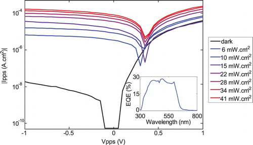
We begin by looking at the typical I–V characteristics for our OPDs as a function of incident illumination intensity in Figure . The OPD output current is modulated by the light intensity; the highest current density at 41 mW cm−2 with a reverse bias of −1 V is 0.135 mA cm−2 (27 μA) while the dark current is as low as 17.5 × 10⁻⁶ mA cm−2. This dark current compares favourably with dark currents of OPDs from all-organic PPSs; these dark currents range from 2.25 mA cm−2 for Jeong et al. with a P3HT/PCBM photodetector [Citation18] to 0.26 mA cm−2 for Someya et al. with their copper phthalocyanine/PTCDI: 3,4,9,10-perylene-tetracarboxylic-diimide photodetector.[Citation19] For the hybrid APS of Tedde et al.,[Citation11] the dark current reached 10−5 mA cm−2 with a photodetector made out of P3HT/PCBM. Our dark current could further be lowered by increasing the photoactive layer thickness to several microns,[Citation20] using different photoactive morphologies,[Citation21] spray coating [Citation22] or double layers using crosslinking agents.[Citation23] In addition, an EQE of 30% was also measured and is presented in Figure (inset). While Someya et al. do not provide their EQE, Jeong et al. showed better EQE performances with 50%. Tedde et al. devices also showed excellent characteristics with EQEs of up to 60%.
Figure 2. IV characteristics of bulk heterojunction photosensors for different illuminations (EQE in inset).
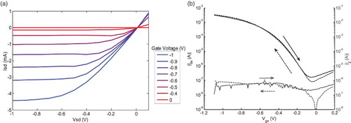
For the transistors used in this study, Figure (a) shows the output characteristics Isd as a function of Vsd at increasing gate voltages. The transistors illustrate gate bias stability and saturation with an increasing Vsd. This saturation occurs at Vsd = −0.5 V for a gate voltage of −1 V. Output currents reached more than −4 mA. Figure (b) shows the transistors' transfer characteristics where the maximum leakage current is Ig∼1 µA. Furthermore, at a sweep rate of 100 mV s−1, there is minimal device hysteresis. The threshold voltage Vth = −0.28 V, mobility µ∼4.3 cm2.V−1 s−1 and Ion/off ratio ∼104 were estimated as illustrated from the transfer curve using the equation µ = I * 2 L/(WC(Vg−Vth)2). It is assumed that at steady state, the capacitance of the dielectric is based on the concentration of ions. As the ionic liquid concentration is same as used as by Lee et al. the value of Ci = 30 µF cm−1 is used for the mobility calculation.[Citation24] The mobility is higher, and the Ion/off ratio lower than the one obtained by Lee et al. [Citation25] who reported µ∼3 cmV−1 s−1and Ion/off ratio ∼105 for a similar P3HT device. This is due to the higher gate leakage currents in these devices Ig∼1 µA compared with Ig∼100 nA measured in their devices. This leakage current could be lowered by a better localisation of the dielectric and gate materials over the channel thus avoiding overlap between the ion-gel and the source–drain electrodes. High-output currents are reached as ions from the ionic liquid dope the semiconductor; these currents should decrease with frequency.[Citation26]
Figure 3. (a) Output characteristics of an UV curable ion-gel OFET (b) Transfer characteristics of an ion-gel dielectric OFET at Vsd = −1 V showing minimal hysteresis and 1 µA maximum leakage current at expected operating voltages. Vg sweep rate was 100 mV s−1.
4. PPS and APS characteristics
The PPS configuration is a readout system (Figure (b)); it does not contain any in-pixel amplification which means that the PPS output current Ipps can only be smaller than the current provided by the photodiode. For Vph = −1 V, Ipps is recorded for several gate voltages and illuminations. The ratio between Ipps with 41 mW cm−2 and dark current lies below 30 at Vg = −1 V which is far lower than the photosensor 6 × 10³ on/off ratio at −1 V reverse bias due to transistor gate leakage current at low illumination. This shows that an ion-gel transistor is not able to act as a switch in a PPS pixel without optimisation of the gate deposition outlined previously. In the APS configuration however, ion-gel transistors are better suited.
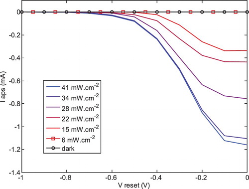
In an APS (Figure (c)) the illuminated photodiode generates a light-dependent voltage Vl which is applied to the gate of the APS transistor Taps, that is, for Taps the Vg = Vl. Thus, the output current Iaps from Taps is a scaled image of the photosensor current, although the amplification is non-linear with the light impinging on the photodiode.[Citation21] The second transistor in this circuit, Treset, acts as a variable load such that the gate voltage Vreset applied to Treset tunes the relationship between Vl and the incident light intensity Iph. Ultimately, Treset is used in the dynamic regime of the APS to unload the charges stored in Taps gate and thus reset the pixel for the next current reading. As such, the state of Taps (on/off) and the resulting photosensor current gain G, defined as the ratio of the output current Iaps to the current Iopd that would be generated by the OPD alone with the same incident light intensity Iph, is controlled by Vreset. The gain can also be tuned through the transistor geometry [Citation11]: a larger W/L ratio for Taps increases the gain.
Figure shows Iaps vs. Vreset for our APS architecture at several different incident illumination intensities. Maximal Iaps is obtained under high illumination and with most positive Vreset, that is, with Treset in its off-state. In this regime there is a clear direct relationship between Iph and Iaps, as one would expect for an amplified OPD signal. Considering the individual curves in Figure , at fixed light intensity, Iaps decreases as Vreset is made more negative. Indeed, as Vreset decreases, the charges stored in the gate capacitance of Taps are unloaded through a Treset in its on state. The pixel's dark current (no illumination) is −40 nA giving an APS on/off ratio, defined as the ratio between Iaps under 41 mW cm−2 and dark, of 3 × 10⁴. Note that this dark current does not arise from gate leakage in Taps because in this instance Vl is ideally zero. Even at high illumination, gate leakage in Taps (∼1 µA) does not contribute strongly to the output signal (∼1 mA). This is a key advantage of the APS over PPS pixels when using ion-gel or other relatively high leakage current transistors.[Citation27] The maximum gain G of this APS was found under a 41 mW cm−2 illumination and was calculated to be 40 with Vaps = Vph = −1 V. Taps is used here in the linear regime; different illuminations give different gate voltages driving Taps which result in a Taps current output modulation. With proper optimisation between the photodiode current window, Iaps, and the transistor geometry, specific illuminations could be detected with optimised gains depending on the target application.
Figure 4. Current Iaps for different photosensor reverse biases Vaps and Treset gate voltages. The maximum Iaps current under dark conditions and 6 mW cm−2 are, respectively, −40 nA and −3.5 µA.
These all-organic APSs characteristics can be compared with Tedde et al.’s devices. While their photodetectors were made out of similar materials, their transistors were fabricated with amorphous silicon as the semiconductor, source and drain electrodes were made out of Cr and the dielectric was a 200 nm Si3N4 layer on glass substrates. The electrical characteristics of this transistor are a saturation current of Isd = −3.4 μA at Vsd = −5 V and a leakage current of 0.57 pA. Using inorganic transistors created on glass, high temperatures could be used and output currents in the microampere range could be reached with a fairly small layout (W/L = 32 µm/4 µm). This hybrid APS, while not flexible, showed a gain of almost 10 at 50 μW cm−2 and was limited to detection of low illuminations. The gains reached by this hybrid APS are in the same range as the gains measured for the APS developed using IG transistors. At similar illumination levels, Tedde et al.'s devices are expected to show much better gains with optimised geometries. The integration time used in this study was 20 μs, while the time needed for the pixel to switch Treset off and measure the signal, including this integration time, was 50 μs. This means that this pixel can be driven at frequencies as high as 20 kHz which is far higher than the frequencies reached by the pixel described in this paper. With state-of-the-art ion-gel transistors, it is believed that the same kind of performances can be reached.
5. Conclusion
In summary, we have shown the electro-optical characteristics of a low-voltage, all-organic APS with a gain of 40. This light signal amplification is possible, thanks to the use of low-voltage OFETs with ionic dielectric. The APS layout allows the output signal to be free from gate leakage current under low illumination. One of the advantages of the APS lies in the fact that G can be tuned through the transistor geometry.[Citation11] A larger W/L ratio for the channel increases the gain. As all materials are solution processable organics and processes made around room temperature, this pixel layout is attractive for low-cost and flexible devices needing photodetection which include chemiluminescence detection,[Citation28] emotional lighting [Citation29] and X-ray photodetectors.[Citation20] Ion-gel transistors are useful for this APS configuration as the driving voltages of these transistors match the safe operating voltages of OPDs. The devices being fabricated on flexible PI and PET, further tests will characterise the flexibility of such APS devices.
Acknowledgements
We acknowledge the Australian Research Council (FT0990285). This work was performed in part using the NSW node of the Australian National Fabrication Facility (ANFF).
Disclosure Statement
No potential conflict of interest was reported by the author(s).
References
- Choi M-C, Kim Y, Ha C-S. Polymers for flexible displays: from material selection to device applications. Prog Polym Sci. 2008;33:581–630. doi: 10.1016/j.progpolymsci.2007.11.004
- Hauch JA, Schilinsky P, Choulis SA, et al. Flexible organic P3HT:PCBM bulk-heterojunction modules with more than 1 year outdoor lifetime. Sol Energ Mat Sol C. 2008;92:727–731. doi: 10.1016/j.solmat.2008.01.004
- Cantatore E, Geuns TCT, Gelinck GH, et al. A 13.56-MHz RFID system based on organic transponders. IEEE J Solid-St Circ. 2007;42:84–92. doi: 10.1109/JSSC.2006.886556
- Cho JH, Lee J, Xia Y, et al. Printable ion-gel gate dielectrics for low-voltage polymer thin-film transistors on plastic. Nat Mater. 2008;7:900–906. doi: 10.1038/nmat2291
- Choi JH, Lee SW, Kar JP, et al. Random network transistor arrays of embedded ZnO nanorods in ion-gel gate dielectric. J Mater Chem. 2010;20:7393–7397. doi: 10.1039/c0jm01313g
- Herlogsson L, Crispin X, Robinson ND, et al. Low-voltage polymer field-effect transistors gated via a proton conductor. Adv M. 2007;19:97–101. doi: 10.1002/adma.200600871
- Ng TN, Wong WS, Lujan RA, Street RA. Characterization of charge collection in photodiodes under mechanical strain: comparison between organic bulk heterojunction and amorphous silicon. Adv Mater. 2009;21:1855–1859. doi: 10.1002/adma.200803046
- Ahn SI, Kim WK, Ryu SH, et al. OLED with a controlled molecular weight of the PVK (poly(9-vinylcarbazole)) formed by a reactive ink-jet process. Org Electron. 2012;13:980–984. doi: 10.1016/j.orgel.2012.02.016
- Xia Y, Zhang W, Ha M, et al. Printed Sub-2 V Gel-electrolyte-gated polymer transistors and circuits. Adv Funct Mater. 2010;20:587–594. doi: 10.1002/adfm.200901845
- Tong X, Forrest SR. An integrated organic passive pixel sensor. Org Electron. 2011;12:1822–1825. doi: 10.1016/j.orgel.2011.07.012
- Tedde S, Zaus ES, Furst J, Henseler D, Lugli P. Active pixel concept combined with organic photodiode for imaging devices. IEEE Electr Device L. 2007;28:893–895. doi: 10.1109/LED.2007.905425
- Graf H-G, Harendt C, Engelhardt T, et al. High dynamic range CMOS imager technologies for biomedical applications. IEEE J Solid-St Circ. 2009;44:281–289. doi: 10.1109/JSSC.2008.2007437
- Hartley L, Kaler KVIS, Yadid-Pecht O. Hybrid Integration of an active pixel sensor and microfluidics for cytometry on a chip. IEEE T Circ Syst I: Regular Papers. 2007;54:99–110. doi: 10.1109/TCSI.2006.887456
- Ma W, Yang C, Gong X, Lee K, Heeger AJ. Thermally stable, efficient polymer solar cells with nanoscale control of the interpenetrating network morphology. Adv Funct Mater. 2005;15:1617–1622. doi: 10.1002/adfm.200500211
- Agostinelli T, Campoy-Quiles M, Blakesley J, Speller R, Bradley D, Nelson J. A polymer/fullerene based photodetector with extremely low dark current for x-ray medical imaging applications. Appl Phys Lett. 2008;93: 203305-203305-203303. doi: 10.1063/1.3028640
- Lee SW, Lee HJ, Choi JH, et al. Periodic array of polyelectrolyte-gated organic transistors from electrospun poly (3-hexylthiophene) nanofibers. Nano Lett. 2009;10:347–351. doi: 10.1021/nl903722z
- Briseno AL, Roberts M, Ling M-M, Moon H, Nemanick EJ, Bao Z. Patterning organic semiconductors using “dry” poly(dimethylsiloxane) elastomeric stamps for thin film transistors. J Am Chem Soc. 2006;128:3880–3881. doi: 10.1021/ja058226v
- Jeong SW, Jeong JW, Chang S, Kang SY, Cho KI, Ju BK. The vertically stacked organic sensor-transistor on a flexible substrate. Appl Phys Lett. 2010;97:253309. doi: 10.1063/1.3530448
- Someya T, Kato Y, Iba S, et al. Integration of organic FETs with organic photodiodes for a large area, flexible, and lightweight sheet image scanners. IEEE T Electron Dev. 2005;52:2502–2511. doi: 10.1109/TED.2005.857935
- Ng TN, Wong WS, Chabinyc ML, Sambandan S, Street RA. Flexible image sensor array with bulk heterojunction organic photodiode. Appl Phys Lett. 2008;92:213303. doi: 10.1063/1.2937018
- Agostinelli T, Campoy-Quiles M, Blakesley JC, Speller R, Bradley DDC, Nelson J. A polymer/fullerene based photodetector with extremely low dark current for x-ray medical imaging applications. Appl Phys Lett. 2008;93:203305. doi: 10.1063/1.3028640
- Tedde SF, Kern J, Sterzl T, Fürst J, Lugli P, Hayden O. Fully spray coated organic photodiodes. Nano Lett. 2009;9:980–983. doi: 10.1021/nl803386y
- Keivanidis PE, Khong S-H, Ho PKH, Greenham NC, Friend RH. All-solution based device engineering of multilayer polymeric photodiodes: minimizing dark current. Appl Phys Lett. 2009;94: 173303–173303. doi: 10.1063/1.3120547
- Lee SW, Lee HJ, Choi JH, et al. Periodic array of polyelectrolyte-gated organic transistors from electrospun poly(3-hexylthiophene) nanofibers. Nano Lett. 2010;10:347–351. doi: 10.1021/nl903722z
- Lee SW, Kim BS, Park JJ, et al. High performance foldable polymer thin film transistors with a side gate architecture. J Mater Chem. 2011;21:18804. doi: 10.1039/c1jm13079j
- Lee J, Kaake LG, Cho JH, Zhu XY, Lodge TP, Frisbie CD. Ion gel-gated polymer thin-film transistors: operating mechanism and characterization of gate dielectric capacitance, switching speed, and stability. J Phys Chem C. 2009;113:8972–8981. doi: 10.1021/jp901426e
- Herlogsson L, Noh YY, Zhao N, Crispin X, Sirringhaus H, Berggren M. Downscaling of organic field-effect transistors with a polyelectrolyte gate insulator. Adv Mater. 2008;20:4708–4713. doi: 10.1002/adma.200801756
- Wang X, Hofmann O, Das R, et al. Integrated thin-film polymer/fullerene photodetectors for on-chip microfluidic chemiluminescence detection. Lab Chip. 2007;7:58–63. doi: 10.1039/B611067C
- Jin Wook J, Young Wook P, Tae Hyun P, et al. The emission properties of integrated organic light emitting diodes with organic photo sensor for emotional lighting applications. IEEE Electron Device Lett. 2011;32:348–350. doi: 10.1109/LED.2010.2099099