
 ?Mathematical formulae have been encoded as MathML and are displayed in this HTML version using MathJax in order to improve their display. Uncheck the box to turn MathJax off. This feature requires Javascript. Click on a formula to zoom.
Abstract
Recent progress of high-speed all-optical logic gates based on dual semiconductor optical amplifiers (SOAs) has been reviewed in this article. These schemes include using quantum-dot semiconductor optical amplifier (QD-SOA) and two-photon absorption (TPA). Numerical simulation method was presented by solving the rate equations of gain dynamics in the SOA. Performance of all-optical logic operation is discussed by calculating the quality factor and plotting the eye diagram. Results show that the dual SOA scheme is a promising method for the realization of high-speed all-optical logic systems in the future.
PUBLIC INTEREST STATEMENT
All-optical logic gates operating at high-speed will play important roles in all-optical communications. This paper reviewed recent progress in high-speed all-optical logic gates based on quantum-dot semiconductor optical amplifier (QD-SOA). It covered recent achievements in using QD-SOA, two-photon absorption (TPA) and both to boost optical communication rate to the next level and to increase the quality factor. This paper provides motivation and detailed analysis of the pros and cons of various schemes of the all-optical logic gate. In addition, the numerical simulation of all-optical operation of these schemes are presented. This paper will be interesting to researchers in optical communication community.
1. Introduction
All-optical signal processing is expected to be increasingly important in future ultrahigh capacity telecommunication networks (Hillerkuss et al., Citation2011). Optical communication systems with per-channel capacity of 100 Gb/s are commercially available today and the capacity in research lab has been pushed to ~1 Tb/s. All-optical logic gates operating at high speeds are important components in the optical systems and will play important roles in future all-optical networks, including signal regeneration, all-optical packet routing and data encryption (Dimitriadou, Zoiros, Chattopadhyay, & Roy, Citation2013; Dorren et al., Citation2003; Willner, Khaleghi, Chitgarha, & Yilmaz, Citation2014; Zhang, Li, Hu, & Dutta, Citation2015a). During the past few decades, there have been extensive research on various schemes of optical logic gates including traditional Boolean logic functions such as XOR, OR, AND, INVERT (Bao et al., Citation2014; Chan, Chan, Chen, & Tong, Citation2004; Dimitriadou & Zoiros, Citation2013b, Citation2013a, Citation2012; Fu, Hu, & Gong, Citation2013; Hendrickson et al., Citation2013; Kotb & Zoiros, Citation2013, Citation2014; Li, Hu, Zhang, & Dutta, Citation2015; Li, Ma, Hu, & Dutta, Citation2012; Ma, Chen, Sun, & Dutta, Citation2010; Sun, Wang, Dong, & Dutta, Citation2005; Zhang, Li, Hu, & Dutta, Citation2015b). These schemes include using light beam interference in silicon photonic crystal (Fu et al., Citation2013), photonic crystal ring resonator (Bao et al., Citation2014), four-wave mixing in semiconductor optical amplifier (SOA) (Chan et al., Citation2004), binary phase shift keyed signal (Li et al., Citation2015), single semiconductor optical amplifier (Dimitriadou & Zoiros, Citation2013b, Citation2013a, Citation2012), and dual semiconductor optical amplifier Mach-Zehnder interferometer (SOA-MI) (Li et al., Citation2012; Sun et al., Citation2005; Zhang et al., Citation2015b). These schemes will require high-speed optical pulse train with an ultra-short pulse width as the data carriers. Significant progress in the generation of ultra-short pulse at high repetition rate (Hu, Zhang, Li, & Dutta, Citation2016; Leaird et al., Citation2001; Li et al., Citation2016; Zhang, Hu, Li, & Dutta, Citation2016; Zoiros et al., Citation2000). Among these schemes, the SOA-based MZI has the advantage of being stable, compact, and simple, which has been demonstrated to be capable of all-optical switching such as XOR, Set-Reset and flip-flop (Li et al., Citation2012; Ma et al., Citation2010; Sun et al., Citation2005; Zhang et al., Citation2015b). Schemes based on dual SOA-MZI (using SOAs with conventional double heterostructure active region) have been demonstrated to be capable of operating at 80 Gb/s (Ma et al., Citation2010; Sun et al., Citation2006). Faster operations will result in an unacceptably high bit error rate (BER) and pattern effects.
Recently, the operation speed of the dual SOA-MZI-based optical logic gates has been enhanced to 250 Gb/s using of SOAs based on quantum-dot (QD) active region and the two-photon absorption (TPA) related fast carrier recovery (Hu, Zhang, & Zhao, Citation2017; Li et al., Citation2012; Ma et al., Citation2010; Zhang et al., Citation2015a). QD-SOAs have high saturated output power, low noise figure, fast carrier relaxation rate between QD energy states and a much smaller heating impact on gain and phase recovery times which makes them suitable for high-speed Boolean logic operations (Berg & Mork, Citation2004; Ma et al., Citation2010). QD-SOA shows good potential to operate at high-speed data rates with good quality factor. The QD excited state carriers can act as a reservoir which results in an ultrafast gain recovery. The other method involves the use of two-photon absorption (TPA) effect which is an ultrafast nonlinear process in SOA under the existence of high-intensity ultrashort pulses. With a high-intensity pump light injected into SOA, a fast-changing TPA-induced phase shift becomes dominant in the total phase change experienced by a weak probe signal (Dorren et al., Citation2004; Kotb & Zoiros, Citation2014; Zhang et al., Citation2015b). As a result, the SOA will quickly respond to the injected short pulse in the active region which makes it suitable for high-speed operation. Several researchers have demonstrated that all-optical logic gates based on TPA effect in common bulk SOA are capable of handling data at the speed up to 250 Gb/s. TPA also has an effect on QD-SOA-based devices. During the propagation of sub-picosecond optical pulses, TPA will generate carriers in the bulk region of the QD-SOA, which also contributes to the carrier dynamics (Ju et al., Citation2006, Citation2006; Zhang & Dutta, Citation2018). By taking TPA into account, Ju et al. demonstrated that the pattern effects are reduced when a train of optical pulses is injected in a QD-SOA; thus, it is possible to operate at a higher speed (Ju et al., Citation2006). Ju’s simulation also has its limitations. It neglects gain saturation and nonlinear effects and is only based on inter-band carrier transitions. These effects dominate the device’s gain dynamics above a certain input power level.
In this work, high-speed all-optical XOR operation based on these three schemes is reviewed. Rate equation approach is discussed, which has been widely used to simulate the carrier dynamics on SOA systems assuming ultrafast dynamics. These schemes provide promising methods for the realization of high-speed all-optical logic operation in future telecommunication systems.
2. Working principle
Figure presents a schematic diagram for all-optical XOR gate based on dual SOA-MZIs. The principle of logic XOR operation utilizing the cross gain modulation (XGM) and cross-phase modulation (XPM) processes in SOAs has been well discussed and analyzed in Refs (Dutta & Wang, Citation2006; Dutta & Zhang, Citation2018; Sunet al., Citation2005). As shown in Figure , two identical SOAs are in the two arms of the interferometer. The function of A XOR B is realized as follows: Data streams A and B are carried by two optical pulse streams at wavelength λ1. They are injected into port 1 and 2, respectively. The wavelengths carrying data streams A and B are not necessarily the same. There is a clock stream centered at λ2 injected into port 3 and it is evenly split into the two arms of the MZI. The two beams then interact with data streams A and B and will experience a modulated gain and phase via XGM and XPM process. Initially, the MZI is unbalanced with a phase difference π between these two branches. As the two clock streams travel in the QD-SOAs, their phases and amplitudes are modulated. When they recombine at port 4, their interference will produce different results under different initial +conditions. For example, if the input A is ‘0ʹ and B is ‘0ʹ, then these two clock streams experience the same gain and phase shift in QD-SOA and when they recombine at port 4, and considering a phase difference π as the initial setup, they will undergo destructive interference and the output result is ‘0ʹ. If A is ‘1ʹ and B is ‘0ʹ, the gain and phase modulation of the two clock streams are different and their interference will produce ‘1ʹ. This realizes the functionality of XOR.
After screening the other wavelength using a band-pass filter (BPF), the output power at wavelength λ2 can be expressed as:
where Pcb is the control beam power at port 3, G1 and G2 are the gains from the SOA, which will be provided in the later section. Since the initial phase difference φ0 = π, then Equation (1) becomes:
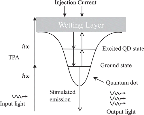
Figure 1. Schematic diagram of the dual SOA-MZI-based XOR gate. BPF: bandpass filter centered at λ2. Two phase shifters are used to induce a π phase difference at two arms.
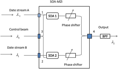
This scheme can also be used to realize the logic AND operation. By inputting data streams A and B into port 1 and 3, we will get a pattern of A AND B out from port 4. A low power CW light is normally injected into port 2 to cancel the background noise of data stream A out.
3. QD-SOA model
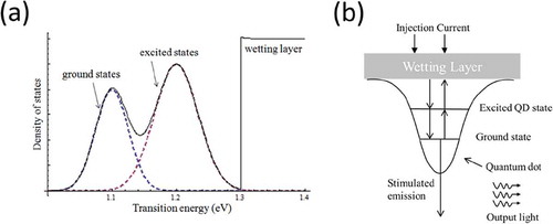
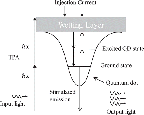
In the dual SOA-based model, QD-SOA has been used to replace the bulk SOA to enhance the all-optical logic operation speed to 250 Gb/s. The commonly discussed InAs/GaAs QD-SOA is a typical device used to construct the all-optical logic gate, in which InAs quantum dots are embedded in GaAs layers (Akiyama, Sugawara, & Arakawa, Citation2007; Ridha, Li, Rossetti, Patriarche, & Fiore, Citation2008; Sugawara et al., Citation2004). The gain of this type of device around 1.55 μm is typically ~15 dB and the noise figure is low at ~7 dB (Akiyama et al., Citation2007). Also, the gain of this device is nearly polarization-independent (Ridha et al., Citation2008). Generally, the three-level rate equation model has been adopted to simulate the carrier transitions in the device. The density of state of the InAs/InGaAsP/InP QD-SOA is shown in Figure ). From the graph, we see the carriers in the QDs are mostly populated on two groups of almost discrete energy levels: QD ground state and QD excited state. The wetting layer has a continuous set of energies, supplying the two levels with carriers through interstate transitions and is able to refill itself using external electric current injection. Figure ) illustrates the optical gain and carrier transition between the wetting layer (WL), the QD excited state (ES), and the QD ground state (GS). The GaAs layer is the “wetting layer” in Figure which is used to feed the ground state and excited state with carriers through interstate recombination. External current is applied to the device and mostly accumulated in the wetting layer. The device gain is determined by the carrier density of the QD ground state. In this model, the barrier dynamics is ignored and it is assumed that carriers are injected directly from the contacts into the WL (Berg, Bischoff, Magnusdottir, & Mork, Citation2001). Since the only recipient of the pump current is the WL, and the QD excited state serves as a carrier reservoir for the ground state with ultra-fast carrier relaxation to the latter, the device gain dynamics is affected by their carrier densities and transition rates.
Figure 2. (a) The QD-SOA density of state as a function of transition energy. (b) A schematic of carrier dynamics in an InAs/GaAs QD-SOA. Quantum dots are embedded in the wetting layer.
The change in carrier densities of the three energy levels are described by the following coupled rate equations (Berg et al., Citation2001; Ju et al., Citation2006; Ma, Sun, Chen, & Dutta, Citation2009):
where w, h, and f represent the occupation probability of the wetting layer, the QD excited state, and ground state, respectively; Nwm, Nesm, and Ngsm are the maximum densities of carriers in each state; the spontaneous radiation lifetime of each state is denoted by τar (“a” being “w”, “es” or “gs”); τa-b denotes the relaxation time between any state “a” and state “b”; Гd is the active layer confinement factor; I is the injected current; a is the differential gain; V is the volume of the active layer; Ad is the effective cross-sectional area of the active layer and S(t) is the total input light power.
The gain of QD-SOA including nonlinear processes such as carrier heating (CH) and spectral hole burning (SHB) effects is expressed as (Akiyama et al., Citation2000; Borri et al., Citation2001):
where N and Nt are the GS carrier density, the transparent GS carrier density, respectively; ε denotes the gain suppression factors. The refractive index of the active region is affected by the injected light and the change of temperature due to carrier heating. As a result, it will cause a phase change to any probe wave injected into the QD-SOA (Li et al., Citation2015):
where GL(t) is the linear gain factor of the device given by eg(t)L, L being the effective length of the active layer; α is the linewidth enhancement factor of the device corresponding to band-to-band transition and αCH is the linewidth enhancement factor of the device related to carrier heating process (Qasaimeh, Citation2005; Vazquez, Nilsson, Zhang, & Galbraith, Citation2006). The linewidth enhancement factor due to spectral hole burning is ~0 (Li et al., Citation2012).
As noted previously, we use a QD-SOA-MZI to realize high speed all-optical XOR and AND operation. The output of this scheme from the combination of two data streams is given by Equation (1), where G1(t) and G2(t) are the calculated total linear gain factors.
Figure 3. Simulation results of XOR gates operating at 250 Gb/s from a dual QD-SOA MZI scheme.
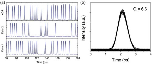
Figure 4. Calculated 250 Gb/s operation quality factor Q at different single pulse energy and transition lifetime from QD excited state to ground state. Injected current density is set to 1.8 kA/cm2. (a): Q factor dependence on single pulse energy, τe-g = 1 ps. (b): Q factor dependence on ES to GS transition lifetime, single pulse energy is 0.5 pJ. Q > 6 is typically needed for bit-error-rate of <10−9. The above figure shows Q > 6 is obtained at 250 Gb/s for pulse width of ~1 ps.
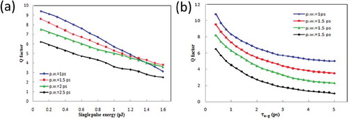
Figure presents the simulation results of the optical XOR gates from the dual QD-SOA MZI schemes. The simulated result is obtained by solving rate equations (3–5) and setting input light beam power within the non-saturated regime. The input Data 1 and Data 2 are generated from a random number generator. The output eye diagram is plotted by superimposing calculated “1” and “0” on each other to show qualitatively the output quality. The output quality can also be quantitively characterized by the Q factor, which is defined as Q = (P1-P0)/(σ1+ σ0) (Dutta & Wang, Citation2006). Here P1 is the average peak power of output signal “1”s and σ1 is the standard deviation of all “1”s. P0 and σ0 are defined analogously for output “0”s. The output bit error rate (BER) is related with the Q factor by: BER ≈ (2π)−1/2exp(-Q2/2)/Q (Ma et al., Citation2010). This scheme operating at 250 Gb/s has a Q factor at 6.6, which indicates a BER below 10−9.
The calculated quality factor shows a significant dependence on pulse energy and transition lifetime from QD excited state to ground state τe-g, as indicated in Figure . The calculation is done with an injected current density of 1.8 kA/cm2. Since the transition lifetime (τe-g) determines the speed of gain and phase recovery speed in the active region, Q-factor is higher for shorter transition times (Figure )). Also, shorter pulse width for a given pulse energy increases Q factor. There is a decrease in output quality with the increase in single pulse energy of the input data (for a given pulse width) (Figure )). As single pulse energy increases, the carrier density of the active region of the device is depleted more; thus, it takes longer to recover to the initial level.
4. TPA model
Another model to realize all-optical logic operation at 250 Gb/s is based on the two-photon absorption of bulk SOA. It is known that TPA of a pump beam can result in the fast phase change of a probe signal. Pump-probe experiments have shown that phase changes take place in a duration ~1 ps or less when the pump and probe signals are injected into a semiconductor optical amplifier (Dorren, Khoe, & Lenstra, Citation2002; Dorren et al., Citation2003, Citation2004). The magnitude of TPA-induced phase shift can be expressed as:
where β is TPA coefficient, α2 is linewidth enhancement factor associated with the TPA process, S(t) is the optical pump pulse intensity, and L is the effective length of SOA active region. The negative sign represents the observation that the TPA-induced phase change is in the opposite direction from that for gain change-induced phase change (Dorren et al., Citation2002, Citation2003). The typical α2 value of bulk SOA is around −4, TPA coefficient β is between 20 and 35 cm−1/GW. The input average power of the SOA used in this paper to obtain significant two-photon absorption is 20 mW in 0.5 ps (FWHM) which corresponds to a peak power of 160 mW at 250 Gb/s. For SOA with an effective length of 7 mm, TPA coefficient β = 30 cm−1/GW, and α2 = −4; the peak phase change experienced by the probe is ~0.4π. The induced phase changes are large enough for temporal interference of probe pulse traveling through the two arms of the MZI (Ma, Chen, & Dutta, Citation2009; Zhang et al., Citation2015b).
The optical powers needed for XGM (cross gain modulation) and XPM (cross-phase modulation) are considerably smaller (~1 mW). Thus, both XGM and XPM are present when the SOA is used in the MZI configuration to form the logic gates. However, these processes are proportional to the power and are slow (timescale ~20 ps) compared to TPA-related phase change which is fast (timescale (~0.5 ps) and is proportional to the square of the power. Thus, high powers are necessary for TPA-based MZI. The input average power of the SOA used to obtain significant two-photon absorption is 20 mW, which corresponds to a peak power of 160 mW at 250 Gb/s when the input pulse width is 0.5 ps. This peak power seems high at first glance; however, several studies have reported measurements on SOAs with high optical peak power. Thus, a few hundred mW of peak power in an ultra-short pulse is acceptable for SOAs. The effect of other nonlinearities such as four-wave mixing (FWM) is eliminated (or minimized) in the output with the use of a bandpass filter.
This scheme also utilizes XPM process in SOAs to realize logic operation. The major difference is that the input data pulses are of sufficiently short duration and has higher power; as a result, the pulses are of higher intensity to produce two-photon absorption and the resulting fast phase change. The average power of the data pulses is about a factor of 20 higher than that used in QD-SOA scheme and the pulse duration is shorter (<1ps). The output of the MZI in this scheme is given by the same equation as Equation (1); however, the temporal gain and phase change in the SOA satisfies the temporal gain rate equations (Mecozzi & Mork, Citation1997)
where h(t) is an integral of optical gain over the length of SOA and htotal equals the sum of hl, hCH, and hSHB. τc is the carrier lifetime, exp[h0] = G0 is the unsaturated power gain and Esat is the saturation energy of the SOA. Esat = Psat τc, Psat is the SOA’s saturation power. P(t) = k S(t) is the input pump power inside the SOA active region, k is the SOA active region cross section, here we use 0.5 μm2. S(t,0) is the instantaneous input optical intensity inside the SOA and hl, hCH, hSHB are the h-factor values for carrier recombination, carrier heating (CH) and spectral hole burning (SHB) respectively. Eqs. (10) and (11) account for the intra-band carrier dynamics (i.e. carrier heating and spectral hole burning effects). For the β value used here (20 cm/GW), the change in intensity due to two-photon absorption is low; hence, that term can be neglected in this model. The carrier density induced phase change is given by:
where α is the traditional linewidth enhancement factor, αCH is the carrier heating linewidth enhancement factor.
The calculated change in gain and phase as a function of time when a pulse train at 250 GHz is injected into the SOA is shown in Figure . It shows that the dominant phase change is due to two-photon absorption. The pulse width (full width at half maximum) is 0.5 ps, the average power is 21 mW and the SOA cross section is 0.5 μm2.
Figure 5. Calculated gain and phase change in an SOA due to a series of pulses shown in (a). (b) Gain modulation as a function of time, (c) phase modulation due to gain modulation as a function of time. The gain plotted is the value of G. (d) total phase modulation including two-photon absorption as a function of time. Note the periodic total phase change is primarily due to two-photon absorption in (d).
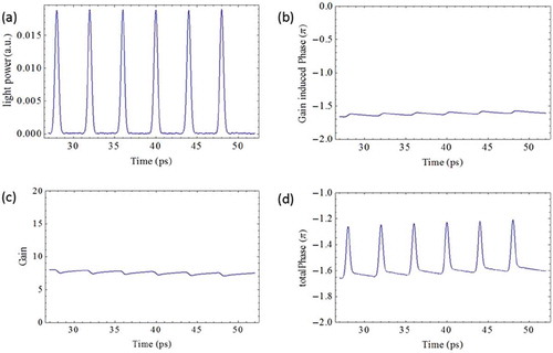
Figure 6. Simulation results of XOR gates operating at 250 Gb/s from a TPA based dual SOA MZI scheme. Data A and Data B are shown on the left. XOR and an eye pattern (after 100 pseudo-random A and B bits) are shown on the right.
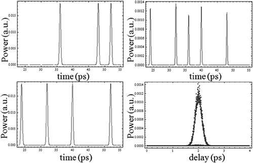
Figure 7. The calculated quality factor Q at different operating bit-rates and different input data stream average powers. Q > 6 is typically needed for bit-error-rate of <10−9. The above figure shows Q > 6 is obtained at 250 Gb/s for input powers of 24 dBm.
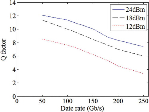
Figure shows the calculated XOR results for 250 Gb/s input data with Gaussian shapes. Signal A has (00001000011) pattern and signal B has (10010010001) pattern. Data streams A and B are on the left and the XOR output is on the upper right. The bottom right shows the eye diagram for an input of 100 random A and 100 random B bits. The Q-factor dependence on data rate and input peak power is presented in Figure . It is shown that, for sufficiently large input power (average power > 18 dBm), this TPA scheme has good quality (Q > 6) at high data rates up to 250 Gb/s. This can be explained as at low power levels, the phase due to TPA is small, and the pattern effect due to slower gain change-induced phase change is more significant. As the injected power increases, the TPA induced fast phase modulation becomes a major contribution of the total phase shift, and the pattern effect becomes relatively small, resulting in higher Q-factor.
Figure 8. A schematic of carrier dynamics with TPA in an InAs/GaAs QD-SOA.
5. TPA in QD-SOA
In the previous QD-SOA rate equation model provided in section 3, the effect of TPA is not considered. However, during the propagation of sub-picosecond optical pulses, two-photon absorption (TPA) will also generate carriers in the bulk region of the QD-SOA, which contributes to the carrier dynamics. Berg et al. (Berg et al., Citation2001) claimed that QD-SOA does not support terabit all-optical logic operation due to the slow recovery of carriers in wetting layers. However, in their model, they assumed that the direct injection of carriers into the wetting layer of a QD-SOA was only from the injected current. By taking TPA into account, Ju et al. demonstrated that the pattern effects are reduced when a train of optical pulses is injected in a QD-SOA; thus, it is possible to operate at a higher speed (Ju et al., Citation2006).
To include the TPA in the QD-SOA model, Equation (3) is modified to
where κ is the TPA coefficient and S(t) is the total input light power (Thapa, Zhang, & Dutta, Citation2018; Zhang, Thapa, & Dutta, Citation2018). The TPA generated carriers are taken into account by the additional term in the end. Figure depicts the carrier dynamics in QD-SOA considering the effects of TPA. The device gain is determined by the carrier density of the QD ground state. The TPA generates carriers in the bulk region. These carriers then relax to the WL, and eventually are captured into QDs on ultrafast timescale (Ju et al., Citation2006). This model ignores the barrier dynamics and assumes that carriers are injected directly from the contacts into the WL (Berg et al., Citation2001).
Figure 9. Simulation results of XOR gates operating at 320 Gb/s without the consideration of TPA. The input single pulse energy is 0.5 pJ and pulse width is 1 ps.
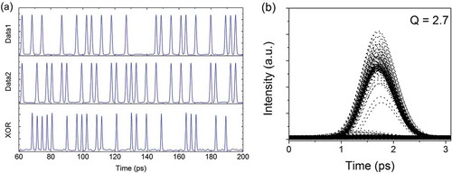
Figure 10. Simulation results of XOR gates operating at 320 Gb/s with the effects of TPA. The input single pulse energy is 0.5 pJ and pulse width is 1 ps.
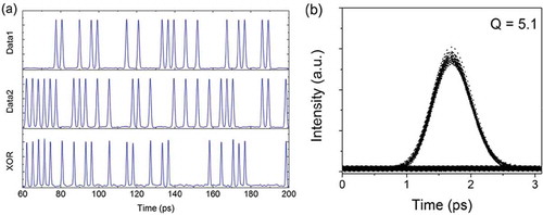
Figure 11. The dependence of Q factor on single pulse energy. The injected current is fixed at 250 mA and pulse width is 1 ps. (b) The dependence of Q factor on injected current. The input single pulse energy is fixed at 0.5 pJ and pulse width is 1 ps. (c) The dependence of Q factor on pulse width/bit period ratio at 320 Gb/s. Note that Q > 6 (needed for bit-error-rate < 10−9) can be obtained. The injected current is fixed at 250 mA and single pulse energy is set at 0.5 pJ. (d) The dependence of Q factor on data rate. The single pulse energy is 0.5 pJ and injected current is 250 mA. The ratio of the pulse width to bit period is fixed.
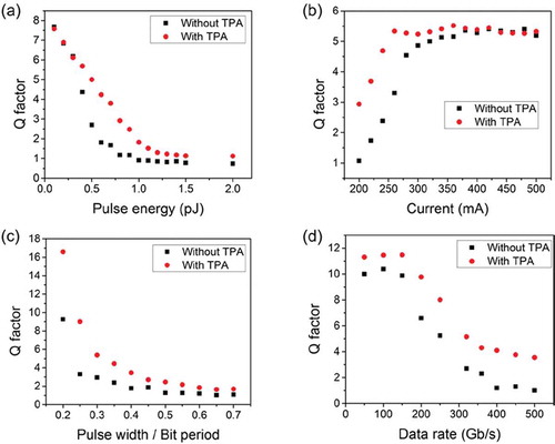
Figure and Figure show the results of XOR performance without and with the consideration of TPA, respectively. In the simulation, a PRBS signal is used as input data and we assume the data stream pulses to be Gaussian pulses. The single pulse energy is 0.5 pJ and full width at half maximum (FWHM) is 1ps. The injected current to the QD-SOA is 250 mA. From the comparison, we can see an obvious improvement of output quality with the consideration of TPA in the model. The eye diagram exhibits an open eye and less noise when the operating speed is 320 Gb/s with the consideration of TPA.
The dependence of Q-factor of XOR result on various parameters is depicted in Figure . The calculated Q factor shows a significant dependence on the injected current, initial pulse width, pulse energy and data rate as suggested in Figure . As we can see in Figure ), by fixing the inject current at 250 mA and FWHM 1ps, the output quality degrades when one increases the single pulse energy of the input data for both with and without TPA cases. Without the effects of TPA, the Q factor drops very fast when pulse energy is increased from 0.1 pJ to 0.5 pJ, while with TPA taken into account, the decrease of Q factor becomes slower. This is easy to understand. As we increase the single pulse energy, the peak power of the pulses is increased. The TPA process is enhanced when the injected pulse train has a higher peak power, which will mitigate the depletion of carrier density of the active region of the device. As a result, the dropping rate of output Q factor will become lower. In Figure ), Q factor increases with the injected current until the current reaches a certain level (~275 mA with TPA and 350 mA without TPA) and then it saturates. With TPA, it saturates at a smaller current level compared with that without TPA. The inject current produces carriers to the wetting layer; thus, in each energy level in the quantum dot, the carrier density is able to recover to its initial state. The more carriers produced, the faster the recovery time will become. This can reduce the pattern effect due to the long recovery time of the logic operation. The TPA process also contributes to the carrier recovery thus the Q factor can saturate at a lower current level than that without TPA. The Q factor decreases with the increase of pulse width and data rate for both cases. The overall Q factor of the TPA case is always higher than that without TPA. This demonstrates that TPA plays an important role in QD gain bleaching and reducing pattern effects for ultrafast optical logic operation.
6. Conclusion
All-optical XOR operating at high speed based on the dual SOA utilizing different models are reviewed. The rate equation models to simulate all-optical logic operation are discussed and presented. The impact on the output qualify (Q factor) from transition lifetime between QD excited state and ground state, pulse width, and single pulse energy are discussed. All-optical XOR gates are the fundamental blocks in the all-optical circuits and future optical communication systems. This dual SOA MZI scheme is simple, compact and is demonstrated to be capable of operating and high-speed which provides a promising method to realize all-optical network in the future.
Additional information
Funding
Notes on contributors
Niloy Dutta
Niloy Dutta is a professor at Department of Physics, University of Connecticut. His research group is doing research on optical communication, all-optical logic, supercontinuum generation, fiber lasers, etc. His group has published many papers about all-optical logic and fiber lasers on international journals and conferences. This paper reviewed the current status in all-optical logic gates and summarized the previous findings from this research group.
References
- Akiyama, T., Kuwatsuka, H., Simoyama, T., Nakata, Y., Mukai, K., Sugawara, M., … Ishikawa, H. (2000). Application of spectral-hole burning in the inhomogeneously broadened gain of self-assembled quantum dots to a multiwavelength-channel nonlinear optical device. IEEE Photonics Technology Letters, 12, 1–14.
- Akiyama, T., Sugawara, M., & Arakawa, Y. (2007). Quantum-dot semiconductor optical amplifiers. Proceedings of the IEEE, 95, 1757–1766.
- Bao, J., Xiao, J., Fan, L., Li, X., Hai, Y., Zhang, T., & Yang, C. (2014). All-optical NOR and NAND gates based on photonic crystal ring resonator. Optics Communications, 329, 109–112.
- Berg, T. W., Bischoff, S., Magnusdottir, I., & Mork, J. (2001). Ultrafast gain recovery and modulation limitations in self-assembled quantum-dot devices. IEEE Photonics Technology Letters, 13, 541–543.
- Berg, T. W., & Mork, J. (2004). Saturation and noise properties of quantum-dot optical amplifiers. IEEE Journal of Quantum Electronics, 40, 1527–1539. doi:10.1109/JQE.2004.835114
- Borri, P., Langbein, W., Hvam, J. M., Heinrichsdorff, F., Mao, M. H., & Bimberg, D. (2001). Spectral hole‐burning and carrier‐heating dynamics in quantum‐dot amplifiers: comparison with bulk amplifiers. Physica Status Solidi (b), 224, 419–423.
- Chan, K., Chan, C.-K., Chen, L. K., & Tong, F. (2004). Demonstration of 20-Gb/s all-optical XOR gate by four-wave mixing in semiconductor optical amplifier with RZ-DPSK modulated inputs. IEEE Photonics Technology Letters, 16, 897–899.
- Dimitriadou, E., & Zoiros, K. (2012). On the design of reconfigurable ultrafast all-optical NOR and NAND gates using a single quantum-dot semiconductor optical amplifier-based Mach–Zehnder interferometer. Journal of Optics, 14, 105401. doi:10.1088/2040-8978/14/10/105401
- Dimitriadou, E., & Zoiros, K. (2013a). Proposal for ultrafast all-optical XNOR gate using single quantum-dot semiconductor optical amplifier-based Mach–Zehnder interferometer. Optics & Laser Technology, 45, 79–88. doi:10.1016/j.optlastec.2012.07.024
- Dimitriadou, E., Zoiros, K., Chattopadhyay, T., & Roy, J. (2013). Design of ultrafast all-optical 4-bit parity generator and checker using quantum-dot semiconductor optical amplifier-based Mach-Zehnder interferometer. Journal of Computational Electronics, 12, 481–489.
- Dimitriadou, E., & Zoiros, K. E. (2013b). All-optical XOR gate using single quantum-dot SOA and optical filter. Journal of Lightwave Technology, 31, 3813–3821. doi:10.1109/JLT.2013.2287905
- Dorren, H., Hill, M., Liu, Y., Calabretta, N., Srivatsa, A., Huijskens, F., … Khoe, G. (2003). Optical packet switching and buffering by using all-optical signal processing methods. Journal of Lightwave Technology, 21, 2.
- Dorren, H., Yang, X., Lenstra, D., De Waardt, H., Khoe, G., Simoyama, T., … Hasama, T. (2003). Ultrafast refractive-index dynamics in a multiquantum-well semiconductor optical amplifier. IEEE Photonics Technology Letters, 15, 792–794.
- Dorren, H., Yang, X., Mishra, A. K., Li, Z., Ju, H., De Waardt, H., … Kawashima, H. (2004). All-optical logic based on ultrafast gain and index dynamics in a semiconductor optical amplifier. IEEE Journal of Selected Topics in Quantum Electronics, 10, 1079–1092. doi:10.1109/JSTQE.2004.835293
- Dorren, H. J., Khoe, G., & Lenstra, D. (2002). All-optical switching of an ultrashort pulse using a semiconductor optical amplifier in a Sagnac-interferometric arrangement. Optics Communications, 205, 247–252.
- Dutta, N. K., & Wang, Q. (2006). Semiconductor optical amplifiers. Singapore: World Scientific.
- Dutta, N. K., & Zhang, X. (2018). Optoelectronic devices. Singapore: World Scientific.
- Fu, Y., Hu, X., & Gong, Q. (2013). Silicon photonic crystal all-optical logic gates. Physics Letters A, 377, 329–333.
- Hendrickson, S., Weiler, C., Camacho, R., Rakich, P., Young, A., Shaw, M., … Jacobs, B. (2013). All-optical-switching demonstration using two-photon absorption and the Zeno effect. Physical Review A, 87, 023808. doi:10.1103/PhysRevA.87.023808
- Hillerkuss, D., Schmogrow, R., Schellinger, T., Jordan, M., Winter, M., Huber, G., … Frey, F. (2011). 26 Tbit s-1 line-rate super-channel transmission utilizing all-optical fast fourier transform processing. Nature Photonics, 5, 364–371.
- Hu, H., Zhang, X., Li, W., & Dutta, N. K. (2016). Hybrid mode-locked fiber ring laser using graphene and charcoal nanoparticles as saturable absorbers. In T. George, A. K. Dutta, M. S. Islam (Eds.), Micro- and Nanotechnology Sensors, Systems, and Applications VIII. International Society for Optics and Photonics. 983630-983630-983638.
- Hu, H., Zhang, X., & Zhao, S. (2017). High-speed all-optical logic gate using QD-SOA and its application. Cogent Physics, 4, 1388156. doi:10.1080/23311940.2017.1388156
- Ju, H., Uskov, A., Li, Z., Vázquez, J. M., Nötzel, R., Lenstra, D., … Dorren, H. (2006). Two-photon-absorption-assisted Tera Hertz optical gain modulation in quantum-dot optical amplifiers. Physica E: Low-dimensional Systems and Nanostructures, 32, 543–546.
- Ju, H., Uskov, A., Nötzel, R., Li, Z., Vázquez, J. M., Lenstra, D., … Dorren, H. (2006). Effects of two-photon absorption on carrier dynamics in quantum-dot optical amplifiers. Applied Physics B, 82, 615–620. doi:10.1007/s00340-005-2107-8
- Kotb, A., & Zoiros, K. (2013). Simulation of all-optical logic XNOR gate based on quantum-dot semiconductor optical amplifiers with amplified spontaneous emission. Optical and Quantum Electronics, 45, 1213–1221.
- Kotb, A., & Zoiros, K. (2014). Performance of all-optical XOR gate based on two-photon absorption in semiconductor optical amplifier-assisted Mach–Zehnder interferometer with effect of amplified spontaneous emission. Optical and Quantum Electronics, 46, 935–944. doi:10.1007/s11082-013-9807-9
- Leaird, D., Shen, S., Weiner, A., Sugita, A., Kamei, S., Ishii, M., & Okamoto, K. (2001). Generation of high-repetition-rate WDM pulse trains from an arrayed-waveguide grating. IEEE Photonics Technology Letters, 13, 221–223. doi:10.1109/68.914327
- Li, W., Hu, H., Zhang, X., & Dutta, N. K. (2015). High speed all optical logic gates using binary phase shift keyed signal based on QD-SOA. International Journal of High Speed Electronics and Systems, 24, 1550005. doi:10.1142/S0129156415500056
- Li, W., Hu, H., Zhang, X., Zhao, S., Fu, K., & Dutta, N. K. (2016). High-speed ultrashort pulse fiber ring laser using charcoal nanoparticles. Applied Optics, 55, 2149–2154. doi:10.1364/AO.55.002149
- Li, W., Ma, S., Hu, H., & Dutta, N. K. (2012). All optical latches using quantum-dot semiconductor optical amplifier. Optics Communications, 285, 5138–5143. doi:10.1016/j.optcom.2012.07.085
- Ma, S., Chen, Z., & Dutta, N. K. (2009). All-optical logic gates based on two-photon absorption in semiconductor optical amplifiers. Optics Communications, 282, 4508–4512.
- Ma, S., Chen, Z., Sun, H., & Dutta, N. K. (2010). High speed all optical logic gates based on quantum dot semiconductor optical amplifiers. Optics Express, 18, 6417–6422. doi:10.1364/OE.18.006417
- Ma, S., Sun, H., Chen, Z., & Dutta, N. (2009). High speed all-optical PRBS generation based on quantum-dot semiconductor optical amplifiers. Optics Express, 17, 18469–18477.
- Mecozzi, A., & Mork, J. (1997). Saturation effects in nondegenerate four-wave mixing between short optical pulses in semiconductor laser amplifiers. IEEE Journal of Selected Topics in Quantum Electronics, 3, 1190–1207.
- Qasaimeh, O. (2005). Linewidth enhancement factor of quantumdot lasers. Optical and Quantum Electronics, 37, 495–507.
- Ridha, P., Li, L., Rossetti, M., Patriarche, G., & Fiore, A. (2008). Polarization dependence of electroluminescence from closely-stacked and columnar quantum dots. Optical and Quantum Electronics, 40, 239–248.
- Sugawara, M., Ebe, H., Hatori, N., Ishida, M., Arakawa, Y., Akiyama, T., … Nakata, Y. (2004). Theory of optical signal amplification and processing by quantum-dot semiconductor optical amplifiers. Physical Review B, 69, 235332.
- Sun, H., Wang, Q., Dong, H., Chen, Z., Dutta, N. K., Jaques, J., & Piccirilli, A. (2006). All-optical logic XOR gate at 80 Gb/s using SOA-MZI-DI. IEEE Journal of Quantum Electronics, 42, 747–751. doi:10.1109/JQE.2006.878184
- Sun, H., Wang, Q., Dong, H., & Dutta, N. (2005). XOR performance of a quantum dot semiconductor optical amplifier based Mach-Zehnder interferometer. Optics Express, 13, 1892–1899. doi:10.1364/opex.13.001892
- Thapa, S., Zhang, X., & Dutta, N. K. (2018). Effects of two photon absorption on pseudo-random bit sequence operating at high speed. Journal of Modern Optics 66(1), 100–108.
- Vazquez, J., Nilsson, H., Zhang, J.-Z., & Galbraith, I. (2006). Linewidth enhancement factor of quantum-dot optical amplifiers. IEEE Journal of Quantum Electronics, 42, 986–993.
- Willner, A. E., Khaleghi, S., Chitgarha, M. R., & Yilmaz, O. F. (2014). All-optical signal processing. Journal of Lightwave Technology, 32, 660–680.
- Zhang, X., & Dutta, N. K. (2018). Effects of two-photon absorption on all optical logic operation based on quantum-dot semiconductor optical amplifiers. Journal of Modern Optics, 65, 166–173. doi:10.1080/09500340.2017.1382595
- Zhang, X., Hu, H., Li, W., & Dutta, N. K. (2016). High-repetition-rate ultrashort pulsed fiber ring laser using hybrid mode locking. Applied Optics, 55, 7885–7891. doi:10.1364/AO.55.007885
- Zhang, X., Li, W., Hu, H., & Dutta, N. K. (2015a). High-speed all-optical encryption and decryption based on two-photon absorption in semiconductor optical amplifiers. Journal of Optical Communications and Networking, 7, 276–285.
- Zhang, X., Li, W., Hu, H., & Dutta, N. K. (2015b). Two-photon absorption-based optical logic. In T. George, A. K. Dutta, M. Saif Islam (Eds.), Micro- and Nanotechnology Sensors, Systems, and Applications VII. International Society for Optics and Photonics. 946731-946731-946710.
- Zhang, X., Thapa, S., & Dutta, N. K. (2018). All-optical logic gates based on quantum-dot semiconductor optical amplifier. International Journal of High Speed Electronics and Systems, 27(01n02), 1840013.
- Zoiros, K., Stathopoulos, T., Vlachos, K., Hatziefremidis, A., Houbavlis, T., Papakyriakopoulos, T., & Avramopoulos, H. (2000). Experimental and theoretical studies of a high repetition rate fiber laser, mode-locked by external optical modulation. Optics Communications, 180, 301–315. doi:10.1016/S0030-4018(00)00708-2