
 ?Mathematical formulae have been encoded as MathML and are displayed in this HTML version using MathJax in order to improve their display. Uncheck the box to turn MathJax off. This feature requires Javascript. Click on a formula to zoom.
Abstract
Integrating diamonds with GaN presents a promising solution for enhancing heat dissipation. However, a critical challenge lies in developing an engineering substrate that facilitates the growth of high-quality GaN epitaxial layers, enabling the production of GaN-based devices with superior thermal management on a large scale. In this study, we have successfully developed an engineering substrate conducive to high-quality GaN growth. This accomplishment was achieved through the direct transfer of a 3 C-SiC thin film, originally grown on Si, to a diamond substrate at room temperature using the surface-activated bonding technique. After the transfer process, we observed the presence of a SiC amorphous layer at the interface, measuring approximately 18.5 nm in thickness. Notably, this thickness reduced to 14.5 nm after annealing at 1100 °C, indicating a transformation from amorphous to polycrystalline SiC due to recrystallization. Furthermore, it is crucial to highlight that no exfoliation of the 3 C-SiC/diamond bonding interfaces was observed even after subjecting them to annealing at 1100 °C. This observation is pivotal for ensuring the high-quality growth of GaN crystals on diamonds. The thermal boundary conductance of the 3 C-SiC/diamond interface reached nearly 93 MW/m2·K, demonstrating significant efficiency for device cooling. These compelling results highlight the potential of the 3 C-SiC/diamond engineering substrate to enable high-performance GaN-based devices, providing significantly enhanced thermal management capabilities. This breakthrough represents a major stride forward in the field.
1. Introduction
Diamond, known for its unparalleled thermal conductivity, presents an ideal material for effective heat dissipation in high-powered semiconductor devices, particularly GaN high electron mobility transistors (HEMTs) [Citation1–4]. However, integrating diamonds with GaN HEMTs demands advanced processing techniques and materials. Two main approaches have been explored: depositing diamond onto exposed GaN surfaces after removing Si from GaN-on-Si substrates, typically utilizing transition layers like SiNx or AlN [Citation3, Citation5, Citation6]; or bonding GaN to a diamond substrate after Si removal, employing adhesion layers such as metal, Si, and SiC [Citation7–9]. The former approach resulted in the production of a 4-inch GaN-on-diamond wafer [Citation10–12] and a low thermal boundary resistance between GaN and diamond achieved by reducing the thickness of the transition layer [Citation13–15]. Nevertheless, it is crucial to highlight that the grain size of polycrystalline diamond near the deposited transition layer was significantly small. Therefore, the thermal conductivity measured in the range of 500–700 W/m·K represents approximately 30% of the value observed in single-crystal diamond [Citation16]. This reduction in thermal conductivity presents a challenge, ultimately impeding effective thermal management. In the latter approach, the “device first” concept was employed, involving GaN device fabrication on a Si substrate before bonding to a diamond substrate [Citation17, Citation18]. This method, however, introduced irregularities and non-uniform strain during GaN device fabrication, negatively impacting device performance and reliability [Citation19]. As a result, it is less suitable for large-diameter wafer applications that require precise uniformity and consistency.
Transferring GaN layers to a diamond substrate before device fabrication proves to be a more effective approach compared to the conventional “device first” method. This “bonding first” concept provides a flat and uniform surface for GaN device fabrication, enhancing overall performance and reliability. It is particularly advantageous for large-diameter wafers, crucial for mass GaN-based device production. However, challenges arise from high-temperature annealing and the necessity to minimize thermal boundary resistance at the interface. Achieving ohmic contacts demands a high-temperature annealing process of about 700 °C [Citation20, Citation21]. Such temperatures can potentially jeopardize the thermal stability of the bonding interface, leading to thermal stress, cracking, and structural disparities between GaN and diamond due to their different crystal structures and thermal expansion coefficients. Furthermore, epitaxial GaN growth typically requires temperatures around 1100 °C [Citation22, Citation23], adding complexity to the bonding process. Nevertheless, reports indicate successful room-temperature bonding of GaN and diamond using a SiC layer with the surface-activated bonding (SAB) method [Citation9]. The interface with the SiC layer demonstrated excellent thermal stability. Additionally, promising results have been reported regarding the seamless transfer of AlGaN/GaN/3C-SiC thin films originally grown on Si (111) to a diamond substrate using a Si intermediate layer, enabling the successful fabrication of GaN HEMTs through the “bonding first” method [Citation24]. This structure exhibited exceptional thermal stability even under extreme conditions up to 1100 °C. The thermal boundary conductance (TBC) of the 3 C-SiC-diamond interface demonstrated efficiency in terms of device cooling [Citation25]. In addition, the cubic polytype of silicon carbide, known as 3 C-SiC, displays a thermal expansion coefficient that falls between those of GaN and diamond, making it a crucial intermediary material [Citation26]. A 1 μm-thick 3 C-SiC thin film has demonstrated exceptional thermal conductivity, reaching up to 200 W/m·K, setting new records [Citation27]. This congruence enabled the creation of an AlGaN/GaN/3C-SiC on diamond structure with both high thermal stability and an elevated TBC.
The difference in crystal structures between GaN and diamond indeed presents a challenge for AlGaN/GaN heterostructure growth directly on a diamond substrate [Citation28, Citation29]. The hexagonal structure of GaN does not readily align with the cubic structure of diamond, making it a technically complex process. The lattice constant of 3 C-SiC, at 0.436 nm, closely aligns with that of GaN at 0.45 nm. The introduction of 3 C-SiC, with its cubic structure, serves as a crucial mediator, bridging the structural mismatch during crystal growth [Citation30]. This pivotal development has paved the way for the successful cultivation of high-quality GaN epitaxial layers on 3 C-SiC/Si substrates. The transfer of 3 C-SiC thin films onto the diamond substrate serves as an engineering solution, streamlining the growth of impeccable GaN epitaxial layers. This technological leap enables the production of high-power and highly efficient GaN devices with diverse structures, built on the proprietary technology of the device manufacturer. Undoubtedly, this marks a significant stride in advancing GaN-based devices, endowing them with enhanced thermal management capabilities.
In this study, we report the production of a 3 C-SiC/diamond structure designed for GaN epitaxial growth. This was achieved through the direct transfer of 3 C-SiC layers, originally cultivated on a Si substrate, to a diamond substrate using the surface-activated bonding (SAB) technique. To comprehensively understand the structural nuances and atomic interactions at the bonding interface, we conducted a systematic investigation employing transmission electron microscopy (TEM) and energy-dispersive X-ray spectroscopy (EDX) after subjecting the interface to annealing at various temperatures. Additionally, we delved into the thermal conductivity (κ) of the 3 C-SiC layer and the TBC at the bonding interface using the time-domain thermoreflectance (TDTR) technique. These analyses shed light on the intricate thermal properties of this composite structure, presenting valuable insights for potential applications in high-performance electronic devices.
2. Experimental
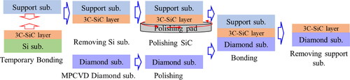
In this study, a 950-nm-thick 3 C-SiC layer grown on a Si (111) substrate using metal-organic chemical vapor deposition (MOCVD), and a diamond substrate synthesized via microwave plasma chemical vapor deposition (MPCVD) were employed. The diamond substrate measured 10 mm × 10 mm × 0.46 mm. The 3 C-SiC layer on Si was temporarily affixed to a support substrate, and subsequently, the Si substrate was removed through a combination of mechanical polishing and wet etching. The support substrate plays a role in maintaining the shape of the 3 C-SiC layer separated from the Si substrate. Before bonding, both the diamond surface and the 3 C-SiC backside were meticulously polished to achieve a flat surface. Atomic force microscopy (AFM) images revealed a notable decrease in the average roughness (Ra) of 3 C-SiC, dropping from 8.44 nm to 0.18 nm after polishing, as shown in . Following this, the diamond and 3 C-SiC layer grown on Si substrates were thoroughly cleaned with acetone, isopropyl alcohol, and a sulfuric acid-hydrogen peroxide mixture. Finally, the diamond and 3 C-SiC layer were directly bonded at room temperature using the surface-activated bonding (SAB) method. After bonding, the handle substrate was carefully removed, resulting in the successful transfer of the 3 C-SiC layer onto the diamond substrate. This transfer process is illustrated in . For a more comprehensive understanding of the diamond bonding procedure, further details can be referred to in the previous work [Citation31–33].
Figure 1. AFM images of 3 C-SiC back side (a) without and (b) with polishing.
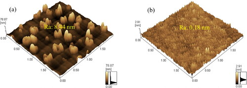
Figure 2. Process for transferring 3 C-SiC layer grown on a Si substrate to a diamond substrate.
The crystal structure and chemical composition of the 3 C-SiC/diamond interface with annealing at various temperatures were scrutinized using TEM and EDX in scanning transmission electron microscopy (STEM) with a JEOL JEM-2200FS analytical microscope. The TEM samples were prepared using the focused ion beam (FIB) technique at room temperature, utilizing the Helios NanoLab600i instrument from Thermos Fisher Scientific. The κ of the 3 C-SiC and TBC of the 3 C-SiC/diamond is determined using the DTR technique. Before TDTR measurements, a ∼90-nanometer-thick layer of aluminum was deposited on the sample surface to serve as the TDTR transducer. TDTR, an ultra-fast laser-based pump-probe technique is adept at assessing the thermal properties of bulk and nanostructured materials [Citation27]. The pump beam cyclically heats the sample surface while the probe beam detects the ensuing temperature variation via thermoreflectance. The resulting signal is processed using a photodetector and a Lock-in amplifier and is then fitted with an analytical heat transfer solution of the sample structure to infer unknown parameters [Citation34]. Additionally, picosecond ultrasonics was employed to determine the thicknesses of the Al and 3 C-SiC layers.
3. Results and discussion
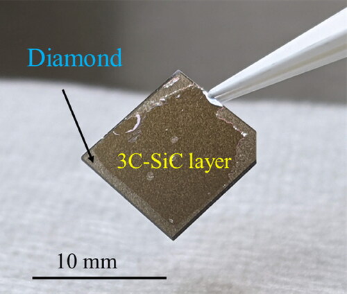
The optical microscopy image in displays the 3 C-SiC/diamond bonded sample. While some layer exfoliation is noticeable, approximately 85% of the layers’ surface area has been effectively transferred to the diamond substrate. This indicates that the bonding process has been largely successful, although there are isolated regions with incomplete bonding. Following the removal of the support substrate, a reduction in the bonded area of about 10% was observed. Bonding interface peeling occurs near the non-bonded area, which is attributed to the weak bonding strength. These results imply that achieving an entirely uniform bonding of 3 C-SiC and diamond might require adjustments in the 3 C-SiC transfer process.
Figure 3. Optical microscopy image of the 3 C-SiC/diamond bonded sample.
show low-magnification cross-sectional TEM images and high-resolution TEM (HRTEM) images taken along the 3 C-SiC zone axis and the diamond [001] zone axis of the as-bonded 3 C-SiC/diamond interface. Notably, an intermediate layer with a thickness of approximately 18.5 nm was observed at the interface. Interestingly, this layer exhibited an amorphous structure, as indicated by the absence of discernible lattice fringes. This amorphous nature was further confirmed by the application of a fast Fourier transform (FFT) analysis. The formation of this amorphous layer is attributed to the Ar fast atom beam irradiation during the bonding process. Similar results have been reported for interfaces involving Si/Si, Si/SiC, and Si/diamond, all of which were fabricated through the SAB method [Citation35–37]. This consistency across interfaces indicates a recurring phenomenon associated with the Ar fast atom beam irradiation during bonding.
Figure 4. TEM and HRTEM images taken along the 3 C-SiC zone axis (a and b) and the diamond [001] zone axis (b and c) of an as-bonded 3 C-SiC/diamond interface. Overlaid FFT images of the interface are presented.
![Figure 4. TEM and HRTEM images taken along the 3 C-SiC [1¯10] zone axis (a and b) and the diamond [001] zone axis (b and c) of an as-bonded 3 C-SiC/diamond interface. Overlaid FFT images of the interface are presented.](/cms/asset/12c5f08b-d1bd-4966-ab28-3bd8bbf9dad0/tfdi_a_2337352_f0004_c.jpg)
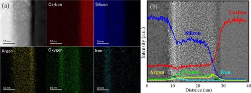
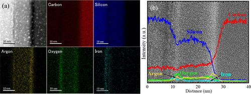
display EDS mappings and X-ray intensity profiles of the as-bonded 3 C-SiC/diamond interface, highlighting the distribution of C, Si, Ar, O, and Fe atoms (represented by red, blue, green, yellow, and cyan respectively). EDS analysis of the as-bonding interface disclosed a distinct heterointerface. In the EDS mappings, it was evident that an oxide layer and an Ar-rich layer formed within the amorphous layer. These were attributed to contaminants introduced by the residual oxygen within the vacuum chamber and Ar fast atom beam irradiation during the bonding process, respectively. Additionally, a minor peak corresponding to the intensity profile of Fe atoms was detected, likely stemming from contaminants within the vacuum chamber. The X-ray intensity profiles further revealed a step-like profile for silicon (Si) atoms within the amorphous layer. Furthermore, the intensity profiles of both carbon (C) and Si atoms exhibited a concave shape in the intermediate layer adjacent to the 3 C-SiC substrate. The observed pattern provides valuable insights into the atomic composition and distribution at the 3 C-SiC/diamond interface.
Figure 5. EDS mapping of the as-bonded 3 C-SiC/diamond interface (a) and X-ray intensity profiles for C, Si, O, Ar, and Fe atoms (represented by red, blue, green, yellow, and cyan respectively) across the interface (b). The inset TEM image provides context by indicating the corresponding location of the measured X-ray intensity profiles for C, Si, O, Ar, and Fe atoms.
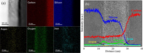
In the case of annealing at 700 °C, show low-magnification cross-sectional TEM images and HRTEM images taken along the 3 C-SiC zone axis and the diamond [001] zone axis of the 700 °C-annealed 3 C-SiC/diamond interface. Notably, no discernible lattice fringes were evident within the intermediate layer, and FFT analysis indicated its continued amorphous state even after annealing at 700 °C. Interestingly, the thickness of the amorphous layer formed at the interface decreased from about 18.5 to 16.5 nm, suggesting a recrystallization process occurred within the amorphous layer. show EDS mappings and X-ray intensity profiles of the 700 °C-annealed 3 C-SiC/diamond interface, highlighting the distribution of C, Si, Ar, O, and Fe atoms (represented by red, blue, green, yellow, and cyan respectively). The EDS mappings persistently indicate the existence of an oxide layer and an Ar-rich layer within the amorphous region. Notably, the intensity profiles of oxygen (O) and iron (Fe) atoms demonstrate a concentration towards the amorphous layer adjacent to the 3 C-SiC side. In contrast, argon (Ar) atoms exhibited higher concentrations near the amorphous layer adjacent to the diamond side. Moreover, the X-ray intensity profiles for Si and C atoms show no significant variation following the annealing process at 700 °C.
Figure 6. TEM and HRTEM images taken along the 3 C-SiC zone axis (a and b) and the diamond [001] zone axis (b and c) of a 700 °C-annealed 3 C-SiC/diamond interface. Overlaid FFT images of the interface are presented.
![Figure 6. TEM and HRTEM images taken along the 3 C-SiC [1¯10] zone axis (a and b) and the diamond [001] zone axis (b and c) of a 700 °C-annealed 3 C-SiC/diamond interface. Overlaid FFT images of the interface are presented.](/cms/asset/ffd1687e-6b3f-4b94-afbe-ff36e9966af6/tfdi_a_2337352_f0006_c.jpg)
Figure 7. EDS mapping of the 700 °C-annealed 3 C-SiC/diamond interface (a) and X-ray intensity profiles for C, Si, O, Ar, and Fe atoms (represented by red, blue, green, yellow, and cyan respectively) across the interface (b). The inset TEM image provides context by indicating the corresponding location of the measured X-ray intensity profiles for C, Si, O, Ar, and Fe atoms.
In the case of annealing at 1100 °C, show low-magnification cross-sectional TEM images and HRTEM images taken along the 3 C-SiC zone axis and the diamond [001] zone axis of the 3 C-SiC/diamond interface. Intriguingly, the thickness of the intermediate layer formed at the interface experienced a further reduction from approximately 16.5 to 14.5 nm. Lattice fringes, indicative of crystalline structure, were discernible within the intermediate layer. The FFT analysis confirmed that the intermediate layer had transitioned into a polycrystalline SiC. This transformation in both the thickness and crystal structure of the intermediate layer can be attributed to the recrystallization process following high-temperature annealing. illustrate EDS mappings and X-ray intensity profiles of the 1100 °C-annealed 3 C-SiC/diamond interface, providing insight into the distribution of C, Si, Ar, O, and Fe atoms (represented by red, blue, green, yellow, and cyan respectively). Notably, the oxide layer persisted, as discerned in the EDS mappings. The intensity profiles of Fe and Ar atoms witnessed a decrease akin to the background signal level, attributed to diffusion after the annealing process. The concave shape observed in the intensity profiles of both C and Si atoms at the interface disappeared. Additionally, the profile intensity of Si atoms within the intermediate layer experienced a significant increase. These findings strongly indicate the transformation of the amorphous layer into a polycrystalline SiC layer due to the high-temperature annealing at 1100 °C.
Figure 8. TEM and HRTEM images taken along the 3 C-SiC zone axis (a and b) and the diamond [001] zone axis (b and c) of a 1100 °C-annealed 3 C-SiC/diamond interface. Overlaid FFT images of the interface are presented.
![Figure 8. TEM and HRTEM images taken along the 3 C-SiC [1¯10] zone axis (a and b) and the diamond [001] zone axis (b and c) of a 1100 °C-annealed 3 C-SiC/diamond interface. Overlaid FFT images of the interface are presented.](/cms/asset/afb2abc7-d0f0-4b35-b2d6-495fb943f325/tfdi_a_2337352_f0008_c.jpg)
Figure 9. EDS mapping of the 1100 °C-annealed 3 C-SiC/diamond interface (a) and X-ray intensity profiles for C, Si, O, Ar, and Fe atoms (represented by red, blue, green, yellow, and cyan respectively) across the interface (b). The inset TEM image provides context by indicating the corresponding location of the measured X-ray intensity profiles for C, Si, O, Ar, and Fe atoms.
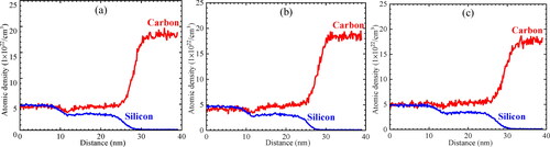
Density profiles of C and Si atoms across the as-bonded, 700 °C-annealed, and 1100 °C-annealed 3 C-SiC/diamond interfaces were shown in , respectively. A slight concave-shaped reduction in the C atomic density in the intermediate layer of the as-bonded interface, adjacent to the 3 C-SiC substrate, was observed. Conversely, the reduction in Si atomic density in the intermediate layer manifested as a step shape. The ratio between the C and Si atomic density was below 1.0 in the intermediate layer. These findings suggest that some Si atoms were removed during the bonding process, resulting in a Si atom-deficient amorphous layer in the 3 C-SiC. This amorphous layer is an atomic intermixing layer consisting of Si and C atoms. The concave-shaped reduction of the C atomic density in the intermediate layer diminished with an increase in the annealing temperature due to the diffusion of C atoms. After annealing at 1100 °C, no reduction in the C atomic density was observed. Meanwhile, the step-shaped reduction in the Si atomic density persisted even after annealing at 1100 °C.
Figure 10. Density profiles of C and Si atoms (red and blue, respectively) across the as-bonded (a), 700 °C-annealed (b), and 1100 °C-annealed (c) 3 C-SiC/diamond interfaces obtained by EDS.
show the picosecond ultrasonics and TDTR measurements on the Al-diamond sample. The echos from the Al-diamond interfaces are used to determine the Al thicknesses. The thermal conductivity (κ) of the diamond substrate is measured to be 1772 W/m·K, which is lower than the thermal conductivity of a perfect single-crystal diamond. The diamond substrate has a yellow color which shows a high concentration of nitrogen impurities in the diamond sample. We attribute the reduced thermal conductivity to the nitrogen impurity in the diamond sample. The Al-diamond thermal boundary conductance (TBC) is determined as 109 MW/m2·K. show the picosecond ultrasonics and TDTR measurements on the Al-3C-SiC-diamond sample. To determine the 3 C-SiC thickness, we use the sound velocity of 3 C-SiC along [111] direction as 12.5 km/s from the literature [Citation38]. The 3 C-SiC film thickness is measured as ∼905 nm. shows the TDTR data fitting of the experimental ratio signal with the analytical heat transfer solution of the 3 C-SiC/diamond sample with annealing at 1100 °C. The bonded 3 C-SiC/diamond interface shows nonhomogeneous and three different spots with high TDTR ratios are measured. The corresponding results are summarized in . The measured thermal conductivity of the 3 C-SiC thin film and the TBC of the 3 C-SiC/diamond interface are determined as 169 W/m·K and 93 MW/m2·K, respectively.
Figure 11. TDTR measurements on the diamond substrate and the 3 C-SiC/diamond sample with annealing at 1100 °C. (a) Picosecond ultrasonics measurements on the diamond substrate sample. (b) the data fitting of TDTR experimental data on the diamond substrate sample. (c) Picosecond ultrasonics measurements on the 3 C-SiC-diamond sample. (d) the data fitting of TDTR experimental data on the 3 C-SiC-diamond sample.
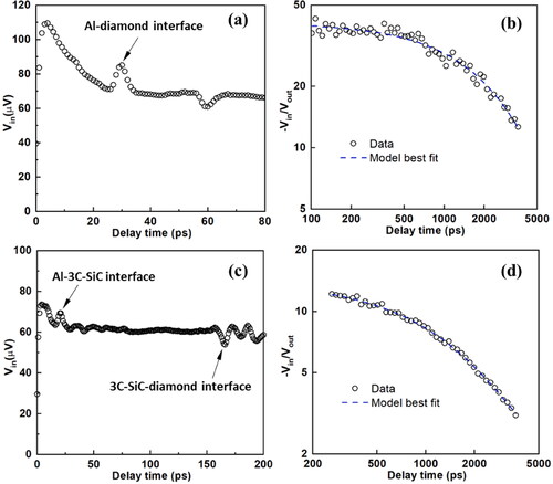
Table 1. Summary of TDTR results of the bonded 3 C-SiC-diamond sample.
We observed the amorphous layer formed at the as-bonded interface had a thickness of 18.5 nm, which is notably thicker compared to the interface fabricated using the SAB method [Citation39–41]. It is worth noting that, in general, an amorphous layer with a thickness typically less than 10 nm is formed at the interface due to the Ar fast atom beam irradiation during the bonding process. This amorphous layer can serve as a buffer layer, contributing to high thermal stability at elevated temperatures [Citation32, Citation42]. A thinner amorphous layer makes it difficult to withstand the high-temperature annealing process for the bonding interface with a larger thermal expansion coefficient between the bonded samples. To achieve higher thermal stability, the bonding interface should have a thicker amorphous layer. The thicker amorphous layer observed at the as-bonded 3 C-SiC/diamond is attributed to the utilization of a higher Ar fast atom irradiation energy. Notably, the thickness of the amorphous layer formed at the bonding interface can be effectively controlled by adjusting the irradiation energy.
The observed reduction in the thickness of the intermediate layer formed at the interface with increasing annealing temperature can be attributed to the recrystallization of the amorphous layer. This transformation leads to the conversion of amorphous SiC into polycrystalline SiC. This phenomenon, induced by plasma irradiation, has been extensively documented in previous studies [Citation26, Citation34, Citation43] observed at the interface. This underscores the successful direct bonding between 3 C-SiC and diamond, demonstrating the robustness of the bonding interface under the high growth temperatures required for GaN epitaxial layer growth, particularly at 1100 °C. The substantial intermediate layer played a crucial role in alleviating the residual stresses resulting from the disparate thermal expansion coefficients between 3 C-SiC and diamond. This observation aligns with findings in the 3 C-SiC/diamond bonding interface with a Si intermediate layer [Citation25].
The TBC of the 3 C-SiC/diamond direct bonding interface is notably lower than the nonequilibrium molecular dynamics simulation value (>1000 MW/m2·K) [Citation44]. This discrepancy is primarily attributed to the presence of the SiC polycrystalline layer at the interface, which adversely affects phonon scattering and reduces the TBC. To mitigate this issue, thinning the thickness of the SiC polycrystalline layer or improving its quality could be potential solutions. In related studies, K. Woo et al. and R. Soman et al. engineered the crystallinity and thickness of the SiC interlayer to achieve high TBC values of approximately 322 and 529 MW/m2·K for the SiC/diamond interface [Citation45, Citation46]. Furthermore, they observed that the TBC decreased with increasing SiC polycrystalline layer thickness and degradation in crystallinity. This trend was attributed to the heightened likelihood of phonon reflection and scattering resulting from these factors. The presence of Ar, Oxygen, and Iron atoms at the interface can be mitigated by enhancing the vacuum level and incorporating a protective cover inside the chamber. However, the influence of these residual atoms on the thermal properties of the interface remains unclear and warrants further investigation in future studies. As reported by K. Woo et al. [Citation45], the main factor affecting TBC is the thickness and crystallinity of the SiC polycrystalline layer. It is essential to reduce the thickness of the SiC polycrystalline layer by optimizing the bonding process and improving the crystal quality of the SiC layer through the post-bonding heat treatment process.
It is crucial to note that the TBC of the 3 C-SiC/diamond direct bonding interface surpasses that (55 MW/m2·K) of the 3 C-SiC/diamond interface with a Si intermediate layer [Citation25] by a factor of 1.69, indicating a substantial enhancement in thermal performance. Furthermore, the TBC of the 3 C-SiC/diamond direct bonding interface is more than 6 times larger than that of the SiC/diamond interface with a metal intermediate layer [Citation18]. This breakthrough holds significant promise for the overall enhancement of bonded interfaces. The process of transferring 3 C-SiC thin films onto a diamond substrate emerges as an engineering solution, streamlining the growth of pristine GaN epitaxial layers. This study presents a compelling avenue for achieving high-quality crystal growth of GaN-based devices on diamond substrates. Leveraging the SiC layer at the bonding interface not only facilitates effective thermal management and heightened heat dissipation but also leads to improved crystal growth, all while mitigating the adverse impacts of thermal stress and associated defects stemming from the bonding process. Continued research and development in this realm could pave the way for the widespread commercialization of GaN-based devices on diamond substrates, unlocking a wide array of applications.
4. Conclusion
We have achieved the successful direct transfer of a 3 C-SiC thin film grown on a Si (111) substrate to a diamond substrate at room temperature using the SAB method. Following the bonding process, an amorphous layer measuring approximately 18.5 nm thick was observed at the interface between the 3 C-SiC and diamond. Subsequent annealing processes led to a reduction in the amorphous layer’s thickness, ultimately resulting in the formation of a polycrystalline SiC layer. Specifically, after annealing at 1100 °C, the thickness decreased to 14.5 nm, indicating a successful transformation. Notably, the bonding interface exhibited exceptional thermal stability, with no voids observed even after the annealing process. This highlights the effectiveness of high-temperature annealing, not only in avoiding detrimental effects like interface cracking or defects but also in enhancing the overall quality of the interface. Furthermore, the high TBC of the 3 C-SiC/diamond direct bonding interface holds significant promise for efficient device cooling. The successful transfer of the 3 C-SiC thin film onto the diamond substrate, used as an engineering substrate, offers immense potential for the mass production of GaN-based devices on diamond substrates. This approach not only provides outstanding thermal management capabilities but also facilitates the growth of high-quality crystals, promising superior device performance.
Acknowledgments
The thermal boundary conductance of the 3C-SiC/diamond interface and the thermal conductivity of the 3C-SiC thin film were measured in collaboration with Dr. Zhe Cheng. 3C-SiC samples were provided by Air Water Co., Ltd.
Author contributions
Ryo Kagawa: Sample fabrication and manuscript writing. Yutaka Ohno: T EM analysis. Yasuyoshi Nagai: EDX analysis. Naoteru Shigekawa: Thermal analysis. Jianbo Liang: Data analysis and manuscript writing.
Additional information
Funding
References
- Liu T, Kong Y, Wu L, et al. 3-inch GaN-on-diamond HEMTs with device-first transfer technology. IEEE Electron Device Lett. 2017;38(10):1–12.
- Hirama K, Taniyasu Y, Kasu M. Electroluminescence and capacitance-voltage characteristics of single-crystal n-type AlN (0001)/p-type diamond (111) heterojunction diodes. Appl Phys Lett. 2011;98:011908-1–3.
- Zhou Y, Ramaneti R, Anaya J, et al. Thermal characterization of polycrystalline diamond thin film heat spreaders grown on GaN HEMTs. Appl Phys Lett. 2017;111:041901-1–5.
- Kuzmik J, Bychikhin S, Pogany D, et al. Thermal characterization of MBE-grown GaN/AlGaN/GaN device on single crystalline diamond. J Appl Phys. 2011;109:107–110.
- Mandal S, Yuan C, Massabuau F, et al. Thick, adherent diamond films on AlN with low thermal barrier resistance. ACS Appl Mater Interf. 2019;11(43):40826–40834.
- Siddique A, Ahmed R, Anderson J, et al. Structure and interface analysis of diamond on an AlGaN/GaN HEMT utilizing an in situ SiN x interlayer grown by MOCVD. ACS Appl Electron Mater. 2019;1(8):1387–1399.
- Wang K, Ruan K, Hu W, et al. Room temperature bonding of GaN on diamond wafers by using Mo/Au nano-layer for high-power semiconductor devices. Scr Mater. 2020;174:87–90.
- Mu F, He R, Suga T. Room temperature GaN-diamond bonding for high-power GaN-on-diamond devices. Scr Mater. 2018;150:148–151.
- Kobayashi A, Tomiyama H, Ohno Y, et al. Room-temperature bonding of GaN and diamond via a SiC layer. Functional Diamond. 2022;2(1):142–150.
- Francis D, Faili F, Babić D, et al. Formation and characterization of 4-inch GaN-on-diamond substrates. Diam Relat Mater. 2010;19(2–3):229–233.
- Cho J, Francis D, Altman DH, et al. Phonon conduction in GaN-diamond composite substrates. J Appl Phys. 2017;121:055105-1–9.
- Käding OW, Rösler M, Zachai R, et al. Lateral thermal diffusivity of epitaxial diamond films. Diam Relat Mater. 1994;3(9):1178–1182.
- Sun H, Simon RB, Pomeroy JW, et al. Reducing GaN-on-diamond interfacial thermal resistance for high power transistor applications. Appl Phys Lett. 2015;106(11):0–4.
- Malakoutian M, Field DE, Hines NJ, et al. Record-low thermal boundary resistance between diamond and GaN-on-SiC for enabling radiofrequency device cooling. ACS Appl Mater Interf. 2021;13(50):60553–60560.
- Yates L, Anderson J, Gu X, et al. Low thermal boundary resistance interfaces for GaN-on-diamond devices. ACS Appl Mater Interf. 2018;10(28):24302–24309.
- Angadi MA, Watanabe T, Bodapati A, et al. Thermal transport and grain boundary conductance in ultrananocrystalline diamond thin films. J Appl Phys. 2006;99:114301-1–6.
- Chao PC, Chu K, Creamer C, et al. Low-temperature bonded GaN-on-diamond HEMTs with 11 W/mm output power at 10 GHz. IEEE Trans Electron Dev. 2015;62(11):3658–3664.
- Minoura Y, Ohki T, Okamoto N, et al. Surface activated bonding of SiC/diamond for thermal management of high-output power GaN HEMTs. Jpn J Appl Phys. 2020;59(SG):SGGD03.
- Nakatsuka O, Kitada H, Kim Y, et al. Characterization of local strain around through-silicon via interconnects by using X-ray microdiffraction. Jpn J Appl Phys. 2011;50(5S1):05ED03.
- Lin ME, Ma Z, Huang FY, et al. Low resistance ohmic contacts on wide band-gap GaN. Appl Phys Lett. 1994;64(8):1003–1005.
- Wang DF, Shiwei F, Lu C, et al. Low-resistance Ti/Al/Ti/Au multilayer ohmic contact to n-GaN. J Appl Phys. 2001;89(11):6214–6217.
- Gibart P. Metal organic vapour phase epitaxy of GaN and lateral overgrowth. Rep Prog Phys. 2004;67(5):667–715.
- Ahn SH, Lee SH, Nahm KS, et al. Catalytic growth of high quality GaN micro-crystals. J Cryst Growth. 2002;234:70–76.
- Kagawa R, Kawamura K, Sakaida Y, et al. AlGaN/GaN/3C-SiC on diamond HEMTs with thick nitride layers prepared by bonding-first process. Appl Phys Express. 2022;15(4):041003.
- Kagawa R, Cheng Z, Kawamura K, et al. High thermal stability and low thermal resistance of large area GaN/3C-SiC/diamond junctions for practical device processes. Small. 2023;20(13):2305574-1–14.
- Moutanabbir O, Gösele U. Heterogeneous integration of compound semiconductors. Annu Rev Mater Res. 2010;40(1):469–500.
- Cheng Z, Liang J, Kawamura K, et al. High thermal conductivity in wafer-scale cubic silicon carbide crystals. Nat Commun. 2022;13:7201-1–9.
- Hirama K, Taniyasu Y, Kasu M. AlGaN/GaN high-electron mobility transistors with low thermal resistance grown on single-crystal diamond (111) substrates by metalorganic vapor-phase epitaxy. Appl Phys Lett. 2011;98:1–4.
- Komiyama J, Abe Y, Suzuki S, et al. Suppression of crack generation in GaN epitaxy on Si using cubic SiC as intermediate layers. Appl Phys Lett. 2006;88:091901-1–3.
- Katagiri M, Fang H, Miyake H, et al. MOVPE growth of GaN on Si substrate with 3C-SiC buffer layer. Jpn J Appl Phys. 2014;53(5S1):05FL09.
- Liang J, Nakamura Y, Zhan T, et al. Fabrication of high-quality GaAs/diamond heterointerface for thermal management applications. Diam Relat Mater. 2021;111:108207.
- Liang J, Masuya S, Kim S, et al. Stability of diamond/Si bonding interface during device fabrication process. Appl Phys Express. 2019;12(1):016501.
- Liang J, Kobayashi A, Shimizu Y, et al. Fabrication of GaN/diamond heterointerface and interfacial chemical bonding state for highly efficient device design. Adv Mater. 2021;33(43):13.
- Cheng Z, Mu F, Yates L, et al. Interfacial thermal conductance across room-temperature-bonded GaN/diamond interfaces for GaN-on-diamond devices. ACS Appl Mater Interf. 2020;12(7):8376–8384.
- Liang J, Miyazaki T, Morimoto M, et al. Electrical properties of Si/Si interfaces by using surface-activated bonding. J Appl Phys. 2013;114:183703-1–6.
- Liang J, Nishida S, Arai M, et al. Effects of thermal annealing process on the electrical properties of p +-Si/n-SiC heterojunctions. Appl Phys Lett. 2014;104:1–5.
- Liang J, Masuya S, Kasu M, et al. Realization of direct bonding of single crystal diamond and Si substrates. Appl Phys Lett. 2017;110:111603-1–4.
- Davydov SY. Effect of pressure on the elastic properties of silicon carbide. Phys Solid State. 2004;46(7):1200–1205.
- Howlader MMR, Suga T, Zhang F, et al. Interfacial behavior of surface activated p-GaP/n-GaAs bonded wafers at room temperature. Electrochem Solid-State Lett. 2010;13(3):H61.
- Higurashi E, Sasaki Y, Kurayama R, et al. Room-temperature direct bonding of germanium wafers by surface-activated bonding method. Jpn J Appl Phys. 2015;54(3):030213.
- Yamajo S, Yoon S, Liang J, et al. Hard X-ray photoelectron spectroscopy investigation of annealing effects on buried oxide in GaAs/Si junctions by surface-activated bonding. Appl Surf Sci. 2019;473:627–632.
- Liang J, Zhou Y, Masuya S, et al. Annealing effect of surface-activated bonded diamond/Si interface. Diam Relat Mater. 2019;93:187–192.
- Shamim MS, Narde RS, Gonzalez-Hernandez JL, et al. Evaluation of wireless network-on-chip architectures with microchannel-based cooling in 3D multicore chips. Sustain Comput: Info Syst. 2019;21:165–178.
- Dong H, Wen B, Zhang Y, et al. Thermal conductivity of diamond/SiC nano-polycrystalline composites and phonon scattering at interfaces. ACS Omega. 2017;2(5):2344–2350.
- Woo K, Malakoutian M, Jo Y, et al. Interlayer engineering to achieve <1 m 2 K/GW thermal boundary resistances to diamond for effective device cooling. International Electron Devices Meeting (IEDM), 2023;9:1–4.
- Soman R, Malakoutian M, Shankar B, et al. Novel all-around diamond integration with GaN HEMTs demonstrating highly efficient device cooling. Technical Digest – International Electron Devices Meeting, IEDM. 2022. p. 3081–3084.