
 ?Mathematical formulae have been encoded as MathML and are displayed in this HTML version using MathJax in order to improve their display. Uncheck the box to turn MathJax off. This feature requires Javascript. Click on a formula to zoom.
ABSTRACT
Harnessing electron spin is crucial in developing energy-saving and high-speed devices for the next generation. In this scheme, visualizing spin-polarized electronic states aids in designing and developing new materials and devices. Spin-resolved photoemission spectroscopy provides information on the spin-polarized electronic states. To investigate the spin-polarized electronic states in microscopic materials and devices, spin-resolved photoemission spectroscopy requires spatial resolution in a sub-micrometer scale. Here we show the imaging-type spin-resolved photoemission microscopy (iSPEM) with an ultraviolet laser developed at the National Institutes for Materials Science (NIMS). Our iSPEM achieves a spatial resolution of 420 nm, drastically improving by more than an order of magnitude compared to conventional spin-resolved photoemission spectroscopy instruments. Besides, the multichannel spin detector significantly reduces the data acquisition time by four orders of magnitude compared to the conventional instruments. The iSPEM machine elucidates the spin-polarized electronic states of sub-micrometer scale materials, polycrystals, device structure samples, and so on, which have yet to be the target of conventional spin-resolved photoemission spectroscopy.
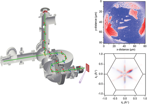
GRAPHICAL ABSTRACT
IMPACT STATEMENT
We have developed an imaging-type spin-resolved photoemission microscopy machine, realizing quick visualization of the spin-polarized electronic states of materials both in real and momentum spaces.
1. Introduction
The convergence of spintronics, topological physics, and quantum technology rapidly expands the potential for innovative changes in modern science and technology. These fields have developed independently, yet merging allows for new approaches. For example, topological spintronics aims to improve information processing and device technology by utilizing electron spins and topological properties [Citation1–3]. Quantum spintronics enables ultrafast quantum computing by controlling the spins in a qubit [Citation4,Citation5]. Using electron spin permits devices with high speed and low power consumption in these technologies.
The spin-polarized electronic bands characterize the properties of functional materials utilizing the spins. Therefore, visualization of spin-polarized electronic states is helpful for the development of new materials and devices. In addition, quantitative evaluation of both spin polarization and spin- orientation is essential for improving the performance of the materials and the devices. Spin- and angle-resolved photoemission spectroscopy (SARPES) is a powerful technique that can independently observe the energy, momentum, and spin of electrons [Citation6]. Here, conventional electronic structure studies using SARPES have been dominated by measurements of spin-polarized band structures of ideal single crystals with sizes typically ranging from several hundred micrometers to several millimeters. SARPES for such ideal systems has significantly contributed to the progress in condensed-matter physics and electronic properties [Citation7–9].
The development of SARPES instruments has been made a great effort, driven by the growing demand to investigate the spin-polarized electronic states of novel materials [Citation10]. In SARPES, the energy and momentum of the photoelectron are examined using a photoelectron analyzer first. Subsequently, the photoelectron is led to the spin detector for spin analysis. Before 2000, SARPES utilized a Mott-type spin detector [Citation11]. The efficiency of the spin detection with the Mott detector was extremely low, necessitating considerable time to acquire the data. The development of a very-low-energy-electron-diffraction (VLEED) type spin detector in the 21st century significantly improved the efficiency of SARPES measurements [Citation12], and SARPES has been widely employed in the study of electronic properties. Besides, the combination of a large hemispherical photoelectron analyzer, the VLEED spin detector, and a high-brilliant vacuum ultraviolet laser realized the high resolution of the SARPES (laser-SARPES), where the energy resolution of 1 meV and a wavenumber resolution of 0.01 Å−1 were achieved [Citation13]. The laser-SARPES has significantly advanced the understanding of the spin-polarized electronic states of topological materials [Citation14–20] and the spin interference in the photoexcitation process [Citation21,Citation22]. In addition to the development of the spin filters, tremendous efforts have been made to improve data acquisition methods in the spin detector. The conventional spin detectors employ a single-channel method, in which photoelectrons of an energy (E) and a momentum (kx, ky) are led to the spin detector, and their spin information is analyzed. Thus, spin-polarized band mapping over the whole Brillouin zone requires enormous time. This situation makes it difficult to systematically investigate the spin-polarized electronic states in various materials. Recently, a multichannel spin detector based on an imaging concept has been developed, allowing for much more efficient data acquisition in SARPES. The multichannel spin detector analyzes the spins of an E–kx or kx–ky image obtained by the two-dimensional photoelectron analyzer simultaneously, of which the measurement efficiency can be four orders of magnitude compared with the single-channel method [Citation23]. As the multichannel spin detectors, spin-polarized low-energy electron scattering (SPLEED) type using W(001) or Au/Ir(001) surfaces [Citation23–26], the VLEED type using an O/Fe(001) surface [Citation27], and an imaging Mott type have been reported [Citation28]. The VLEED-type spin detectors use exchange scattering on ferromagnetic surfaces to distinguish the spins. In contrast, the SPLEED-type spin detectors use spin-dependent diffraction intensity differences on heavy-element surfaces to identify the spins.
Photoemission microscopy offers tremendous opportunities for characterizing the electronic structure of microscopic materials and devices. Spin-integrated photoemission microscopy has been successfully performed at several synchrotron radiation facilities, allowing the measurement of valence bands with sub-micrometer spatial resolution [Citation29–32]. We have recently developed a spin-integrated photoemission microscopy apparatus incorporating a vacuum-ultraviolet laser as a lab-based machine [Citation33]. In the spin-resolved measurements, micro-SARPES has been carried out using a laser focused to 1–50 micrometers [Citation13,Citation34,Citation35]. Using the micro-SARPES, a weak topological insulator phase in bismuth iodate [Citation15] and a higher-order topological insulator phase of bismuth bromide chains [Citation17] have been successfully demonstrated. In general, the sizes of quantum and spintronics materials and devices are less than a few micrometers. Therefore, the spatial resolution of the spin-resolved photoemission microscopy requires less than the sub-micrometers to visualize the spin-polarized electronic state of the microscopic materials and devices. However, such a machine has not been realized so far.
In this article, we report on imaging-type spin-resolved photoemission microscopy (iSPEM) with high spatial resolution developed at the National Institute for Materials Science (NIMS). Our iSPEM machine is equipped with state-of-the-art photoemission microscopy technology and highly efficient spin-resolved data acquisition capability using the multichannel spin detector. We show the spatially resolved spin polarization imaging of the valence states of a polycrystalline iron (poly-Fe) in real-space measurement mode. The spatial resolution of the spin-resolved photoemission microscopy is 420 nm. As a demonstration in momentum space measurement mode, we show the quick imaging of the spin-resolved Fermi surface in the whole Brillouin zone of the bismuth (Bi) (111) surface.
2. Instruments
The iSPEM machine is based on the apparatus reported in reference 33, which consists of three ultra-high vacuum chambers: an analysis chamber, an intermediate chamber, and a sample preparation chamber. The analysis chamber is equipped with a vacuum ultraviolet laser (h = 10.9 eV) (OXIDE, Japan), a helium discharge lamp (He lamp) (h
= 21.2, 40.8 eV) (Scienta Omicron, Sweden), and a mercury vapor lamp (Hg lamp) (h
= 5.2 eV) (FOCUS GmbH, Germany) as excitation light sources. Nano-ESCA made by FOCUS GmbH, Germany, is employed for photoelectron analysis (). Photoelectrons emitted from the sample are accelerated to 12–20 kV by the electrostatic field between the sample and the first lens of the analyzer. Subsequently, the photoelectrons enter the photoelectron emission microscopy (PEEM) column. This PEEM lens system realizes photoelectron microscopy with high spatial resolution. In addition, real-space (x–y) imaging and momentum-space (kx–ky) imaging can be easily switched thanks to the PEEM lens system. Photoelectrons passing through the PEEM column are energy-filtered by an Imaging Double Energy Analyzer (IDEA). An iridium (001) single crystal passivated by a monolayer gold [Au/Ir(001)] is installed at the exit lens section of IDEA. Photoelectrons passing through IDEA are guided to the Au/Ir(001) crystal for spin analysis, where the two-dimensional x–y or kx–ky information is preserved before and after scattering by the Au/Ir(001) crystal. In our setup, the spin detector is arranged to detect the x-component of the spin polarization while the y- and z-components of the spin polarization cannot be measured. A spin-integrated image can be obtained by retracting the Au/Ir(001) crystal. The photoelectrons scattered by the Au/Ir(001) crystal are detected by a two-dimensional imaging unit. Here, we note that Nano-ESCA produces the x–y image in real-space mode and the kx–ky image in momentum-space mode, while the ARPES measurement using a typical hemispherical photoelectron analyzer acquires an E–kx image. Nano-ESCA can simultaneously measure electronic states within kx,y ~ ±6.2 Å−1, significantly reducing the data acquisition time compared with conventional ARPES instruments. Nano-ESCA eliminated the sample rotation for angle-resolved measurements in contrast to the conventional ARPES and SARPES. This capability provides a significant advantage in the band mapping of tiny samples. We note here that the balance between the extraction voltage of the photoelectron analyzer and the kinetic energy of photoelectrons determines the limitation of the measurable momentum range. The photoelectrons with higher kinetic energy cannot be collected even if the extraction voltage is increased.
Figure 1. Overview of the iSPEM instrument with the multichannel spin detector. Green lines represent the photoelectron trajectories.
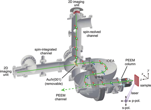
The iSPEM machine adopts the SPLEED-type spin detector using the Au/Ir(001) crystal. In this spin detector, the photoelectrons are reflected by the Au/Ir(001) crystal with the scattering energy at the working points (WP1 and WP2). The photoelectron spins are distinguished using the asymmetry of the spin-dependent scattering intensity at WP1 and WP2. This corresponds to observing the (0 0) spot intensity in low energy electron diffraction (LEED). The exit lens section of IDEA adjusts the energy of the photoelectron incident on the Au/Ir(001) crystal while keeping the image information. The details of the spin detector using the Au/Ir(001) crystal are described in the literature [Citation36,Citation37].
The multichannel spin detector offers the capability of dramatically reducing the data acquisition time compared with the single-channel spin detector. In the iSPEM machine, one obtains a camera image consisting of 1024 1024 ~ 106 data points, where the measurement area has approximately 800,000 data points. Here, if the 1024
1024 data points are binned into 256
256 points, about 50,000 data points are included in the measurement area. The 256
256-point image provides sufficient accuracy for spin-resolved measurements. Therefore, the multichannel spin detector reduces the data acquisition time by four orders of magnitude compared to the single-channel spin detector. Besides, the Nano-ESCA can collect the photoelectrons emitted in the range of 2π sr, which also contributes to the efficient measurements.
We describe how to extract the unknown spin polarization P of the photoelectron from the experimentally measured scattering intensity I1 and I2 at WP1 and WP2 [Citation25,Citation38]. The following equations give the intensities I1 and I2:
where I0 is the unknown photoelectron intensity incident to the Au/Ir(001) crystal, the R1 and R2 are reflectivity at WP1 and WP2, respectively. The values of R1 and R2 are experimentally evaluated using spin unpolarized photoelectrons emitted from a silver polycrystal and are determined to be 0.7% and 2.1%, respectively. S1 and S2 are the spin sensitivities at WP1 and WP2, the so-called effective Sherman functions. The manufacturing test evaluates these values as S1 = −0.68 and S2 = 0.55. From the simultaneous EquationEquations (1(1)
(1) and Equation2
(2)
(2) ), P and I0 are obtained as
By using (3) and (4), the spin-resolved photoelectron images and
are given by
We note that I1 and I2 obtained by the experiments does not directly provide spin-resolved electronic states.
3. Demonstration
3.1. Spin-resolved photoemission microscopy in real space
We show spin-polarized valence state imaging of poly-Fe in the real space mode to characterize our iSPEM. The clean surface of poly-Fe was obtained by repeated cycles of Ar+ sputtering and annealing at 500°C. The Hg lamp was used as an excitation light source. The iSPEM measurements were performed with a field of view (FoV) of 80 µm with the binding energy EB = 0.4 eV at room temperature.
In , we show the scattering energy (Es) dependence of the photoemission microscopy images by the Au/Ir(001) crystal, where only typical examples are displayed. The measurements were performed from the 9.0 eV to 13.0 eV scattering energies with 0.1 eV energy steps. Each image was recorded with a dwell time of 10 sec. In the images of Es = 10.5, 11.3, 11.7 eV, there are several dark gray areas in the light gray area. Light and dark gray areas are not discernible in the image obtained with Es = 12.0 eV. In contrast, the light and dark gray areas in the images of Es = 12.4 and 12.9 eV are reversed. This color contrast reflects the x-component of the spin polarization of magnetic domains in poly-Fe.
Figure 2. (a) Photoemission microscopy images of poly-Fe scattered by the Au/Ir(001) crystal, where only images at selected scattering energies are shown. (b) IV curves, where Iarea1 and Iarea2 are obtained by the summation of the intensity within the area 1 and area 2 shown in (a), respectively. The asymmetry (c) and the relative FOM (d) obtained by the formulas (7) and (8) are displayed.
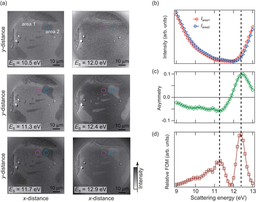
We determine the scattering energies (Es1 and Es2) for spin detection. shows the photoelectron intensities at area 1 and area 2 (Iarea1 and Iarea2) as a function of Es (IV curves). From the IV curves, the asymmetry (Asym) is calculated by
(). Here, we define the relative figure of merit (FOM) as follows:
From the FOM shown in , the working points (WP1 and WP2) for the spin detection are estimated to be Es1 = 11.2 eV and Es2 = 12.4 eV, respectively.
shows a spin-resolved photoemission microscopy image of poly-Fe using the data taken at WP1 and WP2. Here, the absolute value of the spin polarization cannot be determined since the magnetization direction of each magnetic domain of poly-Fe is unknown. By defining the spin quantization axis of the sample, the spin polarization projected on the x-axis can be evaluated quantitatively.
Figure 3. (a) Spin polarization imaging of poly-Fe. The x-spin component is detected. The spin polarization reflecting the magnetic domains in poly-Fe is visualized. Line profiles along #1 (b) and #2 (c) are displayed. Circles give the experimental data. Solid curves represent the fitting results by the step function convoluted with the Gaussian.
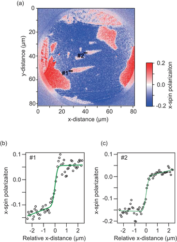
The spatial resolution of our iSPEM is evaluated from the profiles along #1 and #2 in ()). The profiles are fitted by a step function convoluted with a Gaussian. We defined the spatial resolution by the full width at half maximum of the Gaussian. As a result, the spatial resolution at #1 (#2) is estimated to be 420 nm (440 nm). The spatial resolution of this system in spin-integrated photoemission microscopy is 30 nm [Citation33]. The spatial resolution in spin-resolved mode is much lower than that in spin-integrated mode. One reason for this is that the vibration of the instrument affects the spatial resolution of the spin-resolved measurement because the data acquisition time for the spin-resolved measurement is much longer than that for the spin-integrated measurements. Another possible reason is the imperfectness of the Au/Ir(001) surface, which can result in the (00) diffraction spot broadening. A third consideration is the complexity of adjusting the electronic lens system around the Au/Ir(001) crystal at WP1 and WP2, resulting in defocusing the image after reflection by the Au/Ir(001) crystal. Among these causes, the vibration of the equipment reduces the spatial resolution by an order of magnitude (see Supplemental Material and Supplemental Video).
Several magnetic domain patterns are observed in . In particular, the magnetic domains around the center of the image have an elongated shape, similar to those observed in a photoelectron emission microscope combined with X-ray magnetic circular dichroism (XMCD-PEEM) of Co/FeMn [Citation39] and Dy-doped Nd-Fe-B magnets [Citation40], where elongated magnetic domains parallel to the magnetization direction appear. Although the materials are different, these magnetic domain shapes are similar to those in the present results. The iSPEM machine holds the potential to evaluate the magnetic domain shape and the spin polarization of materials in the laboratory without synchrotron radiation.
3.2. Spin-resolved photoemission spectroscopy in momentum space
We show a Fermi surface mapping of a Bi(111) single-crystal film by ARPES and SARPES with the vacuum ultraviolet laser. The Bi(111) surface states are spin-polarized due to strong spin-orbit interaction [Citation41,Citation42], making it suitable for the demonstration of SARPES. The Bi(111) single-crystal film was in situ grown on the Ge(111) substrate. The clean surface of the Ge(111) substrate was obtained by repeated cycles of Ar+ sputtering and annealing up to 600 ºC. Subsequently, a 100-bilayer Bi film was deposited on the Ge(111) substrate at room temperature. The ARPES and SARPES measurements were performed with the experimental geometry shown in . The photoelectrons were excited by the 10.9-eV photons. The light-incident plane is defined as the plane spanned by the light-incident axis and the normal axis of the sample surface. In the present study, we arranged the mirror plane of the sample perpendicular to the light incident plane. The electric field vector of the laser was parallel to the light incident plane (p-polarized light). The sample temperature was kept to 40 K during the measurements. In SARPES, we observed the x-component of the spin polarization. The real space FoV was set to 46 µm.
Figure 4. (a) Schematic drawing of the experimental geometry. Light blue parallelogram represents the mirror plane of crystal, which is perpendicular to both the light incident plane and the electric field vector of the light. Spin-integrated (b) and spin-resolved (c) Fermi surface mappings of Bi(111) are shown. Thin solid lines give edges of the surface brillouin zone (SBZ). (d) Spin texture of the spin-polarized surface states for Bi(111) based on the theoretical calculations [Citation48, Citation49]. The arrows represent the spin direction projected in the plane. Here, the information of the spin polarization value is omitted in this figure.
![Figure 4. (a) Schematic drawing of the experimental geometry. Light blue parallelogram represents the mirror plane of crystal, which is perpendicular to both the light incident plane and the electric field vector of the light. Spin-integrated (b) and spin-resolved (c) Fermi surface mappings of Bi(111) are shown. Thin solid lines give edges of the surface brillouin zone (SBZ). (d) Spin texture of the spin-polarized surface states for Bi(111) based on the theoretical calculations [Citation48, Citation49]. The arrows represent the spin direction projected in the plane. Here, the information of the spin polarization value is omitted in this figure.](/cms/asset/e418b73e-c366-4e59-817b-dccb20700891/tstm_a_2328206_f0004_oc.jpg)
shows the ARPES intensity mapping at the Fermi level of Bi(111). The data acquisition time is 10 sec. Our instrument enables the Fermi surface mapping of the whole Brillouin zone in a single measurement. In , a closed Fermi surface (S1) centered at the point, elliptical Fermi surfaces (S2) and a needle-like Fermi surface (S3) elongated in the
direction are observed. These S1-S3 are the surface states of Bi(111), being in agreement with the previous studies [Citation43,Citation44].
In an ideal model of the spin texture of the spin-orbit coupled surface states, the spin is oriented perpendicular to both the electron momentum and the surface normal [Citation45,Citation46], the so-called spin-momentum locking. Our iSPEM is arranged for the detection of the x-spin polarization. Thus, to observe the spin polarization of the Bi(111) Fermi surfaces elongated to the direction, the SARPES measurements were performed with the experimental geometry that the
axis is parallel to the y-axis. Here, the Bi(111) surface has three-fold rotational symmetry, so that one of the three equivalent
s is parallel to the y-axis as shown in . exhibits the spin-resolved Fermi surface mapping, for which the data acquisition time is 20 min. In the
direction on the ky-axis, the spin polarizations of S1, S2, and S3 are inverted with respect to ky = 0 due to the time-reversal symmetry. On the other hand, in the
direction rotated by ± 60º from the y-axis, the x-component of the spin polarization of S2 is reversed with respect to the
line. The ideal model of the spin-momentum locking cannot explain the observed spin polarization for S2. According to recent experimental and theoretical studies, the spin texture of spin-orbit coupled surface states depends on the symmetry of the surface structure and the details of the electronic orbitals [Citation47]. We refer to theoretical calculations of the spin texture for the Bi(111) surface states to understand our experimental results () [Citation48,Citation49]. The spin of S2 in the
mirror plane is exactly pointing in the direction perpendicular to the mirror plane. The general description of the spin-orbital texture in the mirror plane is described in the reference [Citation21]. On the other hand, the spins are pointing in a different direction from that predicted by the spin-momentum locking model away from the
mirror plane. The experimental results shown in are explained by the projection of the calculated spin texture onto the x-axis.
The x-component of the spin polarization observed in the SARPES measurements qualitatively agrees with theoretical calculations. Here, one should be careful in quantitatively treating the spin polarization of the spin-orbit coupled surface state observed by SARPES, i.e. the direction of the spin vector and the value of the spin polarization. The photoemission process is described by a dipole transition matrix element , where
is the initial state,
the final state, A the vector potential of the light, and p the electron momentum operator. The matrix element contains information not only on the initial state but also on the photoexcitation process. Therefore, the spin polarization of photoelectrons observed by SARPES can be modified due to the matrix element effect, which has been systematically studied in previous studies [Citation21,Citation22,Citation50,Citation51].
A great advantage of the iSPEM machine is the capability of spin-resolved photoemission imaging. Especially in real-space measurements, one can perform spin-resolved photoemission microscopy with high spatial resolution and high efficiency, as demonstrated in . In momentum space measurements, the real-space FoV determines the spatial resolution. The magnification of the real-space FoV can be continuously optimized from a few micrometers to several hundred micrometers, depending on the area of interest, which is another major advantage. In addition, the SARPES measurements in sub-micrometer scale (nano-SARPES) are available using a spot selector (continuously variable iris aperture) although the photoelectron intensity is smaller. Very recently, Xu et al. realized the SARPES measurement with a spatial resolution of less than 1 µm using a focused laser [Citation34]. Their machine employs the single-channel spin detector, and thus the efficiency for the spin detection is four orders of magnitude lower than that using the multichannel spin detector. In our system, however, the spot size of the laser is more than 100 µm, resulting in a photon density reduction of four orders of magnitude for a 1 µm FoV. Therefore, the efficiency of SARPES measurements in the momentum space with 1 µm spatial resolution using our iSPEM would be comparable to the machine reported by Xu et al. The combination of the focused incident light and the iSPEM would permit the nano-SARPES measurements with even higher efficiency and high spatial resolution.
4. Summary and outlook
We have developed imaging-type spin-resolved photoemission microscopy (iSPEM) with a 10.9-eV laser. Thanks to the multichannel spin detector, the data acquisition efficiency in spin-resolved photoemission spectroscopy has been improved by four orders of magnitude compared with the conventional machines using the single-channel one. The PEEM lens system has realized the high spatial resolution in iSPEM. In the real-space mode of iSPEM, the spatial resolution of 420 nm has been achieved, more than an order of magnitude higher than that of the conventional spin-resolved photoemission spectroscopy. In the momentum-space mode of iSPEM, the spin-resolved Fermi surface imaging of Bi(111) has been demonstrated.
The highly efficient spin detection capability and the high spatial resolution of iSPEM enable the observation of the spin-polarized electronic states of tiny samples and inhomogeneous samples, for instance, polycrystalline, powder, and combinatorial samples, which are challenging to measure the electronic states by the conventional spin-resolved photoemission spectroscopy. Besides, visualization of the spin polarization of functional electrons is significant for designing and developing spin-based devices. The iSPEM technique would dramatically advance the study of electronic properties in various materials, such as quantum, magnetic, and low-dimensional materials, as well as in devices utilizing these materials.
Supplemental Material
Download PDF (629.7 KB)Supplemental Material
Download Microsoft Video (AVI) (995.5 KB)Acknowledgements
The authors thank Nils Weber and Fumiya Arai for their technical support in developing the spectrometer. The authors also thank Shingo Takezawa for technical support in preparing the Bi/Ge(111) sample.
Disclosure statement
No potential conflict of interest was reported by the author(s).
Data availability statement
The data that support the findings of this study are available from the corresponding author upon reasonable request.
Supplementary material
Supplemental data for this article can be accessed online at https://doi.org/10.1080/27660400.2024.2328206
Additional information
Funding
References
- Tokura Y, Kawasaki M, Nagaosa N. Emergent functions of quantum materials. Nat Phys. 2017;13(11):1056. doi: 10.1038/nphys4274
- Gilbert MJ. Topological electronics. Commun Phys. 2021;4:70. doi: 10.1038/s42005-021-00569-5
- He QL, Hughes TL, Armitage NP, et al. Topological spintronics and magnetoelectronics. Nat Mater. 2022;21:15. doi: 10.1038/s41563-021-01138-5
- Awschalom DD, Bassett LC, Dzurak AS, et al. Quantum spintronics: engineering and manipulating atom-like spins in semiconductors. Science. 2013;339:1174. doi: 10.1126/science.1231364
- Lu Y, Sigov A, Ratkin L, et al. Quantum computing and industrial information integration: a review. J Ind Inf Integr. 2023;35:100511. doi: 10.1016/j.jii.2023.100511
- Johnson PD. Spin-polarized photoemission. Rep Prog Phys. 1997;60(11):1217. doi: 10.1088/0034-4885/60/11/002
- Okuda T, Kimura A. Spin- and angle-resolved photoemission of strongly spin–orbit coupled systems. J Phys Soc Jpn. 2013;82(2):021002. doi: 10.7566/JPSJ.82.021002
- Lv B, Qian T, Ding H. Angle-resolved photoemission spectroscopy and its application to topological materials. Nat Rev Phys. 2019;1:609. doi: 10.1038/s42254-019-0088-5
- Sobota JA, He Y, Shen ZX. Angle-resolved photoemission studies of quantum materials. Rev Mod Phys. 2021;93:025006. doi: 10.1103/RevModPhys.93.025006
- Okuda T. Recent trends in spin-resolved photoelectron spectroscopy. J Phys Condens Matter. 2017;29(48):483001. doi: 10.1088/1361-648X/aa8f28
- Gay TJ, Dunning FB. Mott electron polarimetry. Rev Sci Instrum. 1992;63:1635. doi: 10.1063/1.1143371
- Okuda T, Takeichi Y, Maeda Y, et al. A new spin-polarized photoemission spectrometer with very high efficiency and energy resolution. Rev Sci Instrum. 2008;79(12):123117. doi: 10.1063/1.3058757
- Yaji K, Harasawa A, Kuroda K, et al. High-resolution three-dimensional spin- and angle-resolved photoelectron spectrometer using vacuum ultraviolet laser light. Rev Sci Instrum. 2016;87(5):053111. doi: 10.1063/1.4948738
- Zhang P, Yaji K, Hashimoto T, et al. Experimental observation of topological superconductivity on iron-based superconductor topological superconductor. Science. 2018;360:182. doi: 10.1126/science.aan4596
- Noguchi R, Takahashi T, Kuroda K, et al. A weak topological insulator state in quasi-one-dimensional bismuth iodide. Nature. 2019;588:518. doi: 10.1038/s41586-019-0927-7
- Zhang P, Wang Z, Wu X, et al. Multiple topological states in iron-based superconductors. Nat Phys. 2019;15:41. doi: 10.1038/s41567-018-0280-z
- Noguchi R, Kobayashi M, Jiang Z, et al. Evidence for a higher-order topological insulator in a 3D material built from van der waals stacking of bismuth-halide chains. Nat Mater. 2021;20:473. doi: 10.1038/s41563-020-00871-7
- Zhang P, Noguchi R, Kuroda K, et al. Observation and control of the weak topological insulator state in ZrTe5. Nat Commun. 2021;12:406. doi: 10.1038/s41467-020-20564-8
- Lin C, Ochi M, Noguchi R, et al. Visualization of the strain-induced topological phase transition in a quasi-one-dimensional superconductor TaSe3. Nat Mater. 2021;20:1093. doi: 10.1038/s41563-021-01004-4
- Yoshizawa S, Kobayashi T, Nakata Y, et al. Atomic-layer rashba superconductor protected by dynamic spin-momentum locking. Nat Commun. 2021;12:1462. doi: 10.1038/s41467-021-21642-1
- Yaji K, Kuroda K, Toyohisa S, et al. Spin-dependent quantum interference in photoemission process from spin-orbit coupled states. Nat Commun. 2017;8(1):14588. doi: 10.1038/ncomms14588
- Kuroda K, Yaji K, Noguchi R, et al. Visualization of optical polarization transfer to photoelectron spin vector emitted from the spin-orbit coupled surface state. Phys Rev B. 2022;105:L121106. doi: 10.1103/PhysRevB.105.L121106
- Kolbe M, Lushchyk P, Petereit B, et al. Highly efficient multichannel spin-polarization detection. Phys Rev Lett. 2011;107(20):207601. doi: 10.1103/PhysRevLett.107.207601
- Tusche C, Ellguth M, Ünal AA, et al. Spin-resolved photoelectron microscopy using a two-dimensional spin-polarizing electron mirror. Appl Phys Lett. 2011;99:032505. doi: 10.1063/1.3611648
- Tusche C, Krasyuk A, Kirschner J. Spin resolved band structure imaging with a high-resolution momentum microscope. Ultramicroscopy. 2015;159:520. doi: 10.1016/j.ultramic.2015.03.020
- Tusche C, Chen YJ, Plucinski L, et al. From photoemission microscopy to an “all-in-one” photoemission experiment. E-J Surf Sci Nanotechnol. 2020;18:48. doi: 10.1380/ejssnt.2020.48
- Ji F, Shi T, Ye M, et al. Multichannel exchange-scattering spin polarimetry. Phys Rev Lett. 2016;116(17):177601. doi: 10.1103/PhysRevLett.116.177601
- Strocov VN, Petrovb VN, Dil JH. Concept of a multichannel spin-resolving electron analyzer based on Mott scattering. J Synchrotron Radiat. 2015;22:708. doi: 10.1107/S160057751500363X
- Dudin P, Lacovig P, Fava C, et al. Angle-resolved photoemission spectroscopy and imaging with a submicrometre probe at the SPECTROMICROSCOPY-3.2L beamline of Elettra. J Synchrotron Rad. 2010;17:445. doi: 10.1107/S0909049510013993
- Rotenberg E, Bostwick A. microARPES and nanoARPES at diffraction-limited light sources: opportunities and performance gains. J Synchrotron Rad. 2014;21:1048. doi:10.1107/S1600577514015409
- Avila J, Razado-Colambo I, Lorcy S, et al. ANTARES, a scanning photoemission microscopy beamline at SOLEIL. J Phys Conf Ser. 2013;425(19):192023. doi: 10.1088/1742-6596/425/19/192023
- Hoesch M, Kim TK, Dudin P, et al. A facility for the analysis of the electronic structures of solids and their surfaces by synchrotron radiation photoelectron spectroscopy. Rev Sci Instrum. 2017;88(1):013106. doi: 10.1063/1.4973562
- Yaji K, Tsuda S. Development of a photoemission microscopy apparatus using a vacuum ultraviolet laser. e-J Surf Sci Nanotechnol. 2024;22:46. doi: 10.1380/ejssnt.2023-066
- Xu RZ, Gu X, Zhao WX, et al. Development of a laser-based angle-resolved-photoemission spectrometer with sub-micrometer spatial resolution and high-efficiency spin detection. Rev Sci Instrum. 2023;94:023903. doi: 10.1063/5.0106351
- Iwata T, Kousa T, Nishioka Y, Laser-based angle-resolved photoemission spectroscopy with micrometer spatial resolution and detection of three-dimensional spin vector. Sci Rep. 2024;14:127. doi: 10.1038/s41598-023-47719-z
- Kirschner J, Giebels F, Gollisch H, et al. Spin-polarized electron scattering from pseudomorphic au on Ir(001). Phys Rev B. 2013;88(12):125419. doi: 10.1103/PhysRevB.88.125419
- Vasilyeva D, Tusche C, Giebels F, et al. Low-energy electron reflection from Au-passivated Ir(001) for application in imaging spin-filters. J Elect Spectr Rel Phenom. 2015;199:10. doi: 10.1016/j.elspec.2014.12.006
- Tusche C, Ellguth M, Krasyuk A, et al. Quantitative spin polarization analysis in photoelectron emission microscopy with an imaging spin filter. Ultramicroscopy. 2013;130:70. doi: 10.1016/j.ultramic.2013.02.022
- Kuch W, Offi F, Chelaru LI, et al. Huge magnetocrystalline anisotropy of x-ray linear dichroism observed on Co ∕ Fe Mn bilayers. Phys Rev B. 2007;75:224406. doi: 10.1103/PhysRevB.75.224406
- Yamaguchi R, Terashima K, Fukumoto K, et al. An XMCD-PEEM study on magnetized Dy-doped Nd-Fe-B permanent magnets. IBM J Res Dev. 2011;55:12. doi: 10.1147/JRD.2011.2159148
- Koroteev YM, Bihlmayer G, Gayone JE, et al. Strong spin-orbit splitting on bi surfaces. Phys Rev Lett. 2004;93(4):046403. doi: 10.1103/PhysRevLett.93.046403
- Hirahara T, Miyamoto K, Matsuda I, et al. Direct observation of spin splitting in bismuth surface states. Phys Rev B. 2007;76:153305. doi: 10.1103/PhysRevB.76.153305
- Hirahara T, Nagao T, Matsuda I, et al. Role of spin-orbit coupling and hybridization effects in the electronic structure of ultrathin bi films. Phys Rev Lett. 2006;97(14):146803. doi: 10.1103/PhysRevLett.97.146803
- Ito S, Feng B, Arita M, et al. Proving nontrivial topology of pure bismuth by quantum confinement. Phys Rev Lett. 2016;117(23):236402. doi: 10.1103/PhysRevLett.117.236402
- Hoesch M, Muntwiler M, Petrov VN. Spin structure of the Shockley surface state on au (111). Phys Rev B. 2004;69(24):241401. doi: 10.1103/PhysRevB.69.241401
- Yaji K, Harasawa A, Kuroda K, et al. Rashba spin splitting of L-gap surface states on Ag(111) and Cu(111). Phys Rev B. 2018;98(4):041404. doi: 10.1103/PhysRevB.98.041404
- Sakamoto K, Kobayashi T, Yaji K, et al. Spin-polarized electrons in atomic layer materials formed on solid surfaces. Prog Surf Sci. 2022;97(3):100665. doi: 10.1016/j.progsurf.2022.100665
- Saito K, Sawahata H, Komine T. Tight-binding theory of surface spin states on bismuth thin films. Phys Rev B. 2016;93(4):041301. doi: 10.1103/PhysRevB.93.041301
- Randeria MT, Feldman BE, Wu F, et al. Ferroelectric quantum hall phase revealed by visualizing Landau level wavefunction interference. Nat Phys. 2018;14(8):796–9. doi: 10.1038/s41567-018-0148-2
- Heinzmann U, Dil JH. Spin–orbit-induced photoelectron spin polarization in angle-resolved photoemission from both atomic and condensed matter targets. J Phys Condens Matter. 2012;24(17):173001. doi: 10.1088/0953-8984/24/17/173001
- Kuroda K, Yaji K, Nakayama M, et al. Coherent control over three-dimensional spin polarization for the spin-orbit coupled surface state of Bi2Se3. Phys Rev B. 2016;94(16):165162. doi: 10.1103/PhysRevB.94.165162