
 ?Mathematical formulae have been encoded as MathML and are displayed in this HTML version using MathJax in order to improve their display. Uncheck the box to turn MathJax off. This feature requires Javascript. Click on a formula to zoom.
Abstract
The properties of graphene, carbon sheets that are only one atom wide, have led researchers and companies to consider its synthesis, properties, and the applications in numerous fields. High-quality graphene is physically powerful, light, nearly transparent, and an exceptional conductor of heat and electricity. Its interactions with other materials and with light and its naturally two-dimensional nature produce unique properties, such as the bipolar transistor effect, ballistic transport of charges, and large quantum oscillations. The following review introduces the many potential applications of graphene.
Introduction
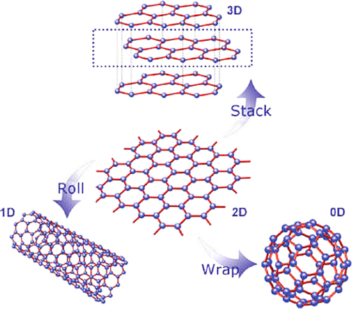
Graphene is a wonder material with many superlatives to its name. It is the thinnest material in the universe and the strongest ever measured. Graphene is a two-dimensional material with layers of carbon atoms that the six pieces of the rings are that together have been (CitationGeim 2009). Graphene, the latest member of carbon allotropes, is truly the basic building block of other important carbon allotropes, including 3D graphite, 1D carbon nanotubes (CNTs), and 0D fullerene (C60) (). Therefore, there has long been an interest of many earlier theoretical studies. Previous experimental works related to it are mostly about graphite intercalation compounds and graphite oxide (CitationDreyer et al. 2010).
Graphene is an exciting material (CitationGeim and Novoselov 2007). It has a large theoretical specific surface area (2630 m2g− 1), high intrinsic mobility (200,000 cm2 v− 1 s− 1) (CitationBolotin et al. 2008, CitationMorozov et al. 2008), high Young's modulus (1.0 TPa) (CitationLee et al. 2008) and thermal conductivity (5000 Wm− 1 K− 1) (CitationBalandin et al. 2008), and its optical transmittance (97.7%) and good electrical conductivity merit attention for applications such as for transparent conductive electrodes (CitationLi et al. 2009), among many other potential applications (CitationZhu et al. 2010).
The most general preparation method of graphene starts from the oxidation and exfoliation of graphite to graphene oxide (GO) (CitationPark and Ruoff 2009, CitationPark et al. 2009). The structure of graphene oxide sheets consists of basal plane of the sheet decorated with hydroxyl and epoxy functional groups, carbonyl groups are present not only as carboxylic acids along the sheet edge but also as organic carbonyl defects within the sheet (CitationStankovich et al. 2007, CitationLerf et al. 1998).
Throughout the past half decade, graphene has been studied in the context of many applications, such as polymer composites, energy-related materials, sensors, “paper”-like materials, field-effect transistors (FETs), and biomedical applications, due to its excellent electrical, mechanical, and thermal properties (CitationGeim and Novoselov 2007, CitationPark and Ruoff 2009). Graphene chemistry has the possibility of playing an ever more important role in future developments, such as stoichiometric derivatives that offer a way to control the electronic structure, which is of interest for many applications including electronics. The reduction of electrically insulating graphene oxide, which is exfoliated from graphite oxide (GO), and use of the colloidal suspensions of reduced graphene oxide are among the most promising ways to produce electrically conducting graphene-based platelets on a large scale (CitationPark and Ruoff 2009, CitationPark et al. 2009, CitationLi et al. 2008, CitationNiyogi et al. 2006, CitationSi and Samulski 2008), and therefore its potential in composites (CitationStankovich et al. 2006, CitationWang et al. 2010, CitationLiang et al. 2009), paper-like materials, and thin films (CitationChen et al. 2008, CitationDikin et al. 2007); as substrates (CitationLee et al. 2010, CitationKim et al. 2010); as a coating layer (CitationHan et al. 2010); and as transparent conductive films (CitationWatcharotone et al. 2007, CitationEda et al. 2008).
High yields of GO monolayers, 0.78 nm in thickness, can be readily prepared by treatment of graphite under strongly acidic and oxidizing conditions (CitationHummers and Offeman 1958, CitationPatil et al. 2009). The GO single sheets can be readily dispersed in water and mounted onto substrates using spin-, dip-, and spray-coating techniques, and reduced in situ to produce isolated graphene monolayers or transparent 2D films (CitationWatcharotone et al. 2007, CitationGómez-Navarro et al. 2007, CitationWang et al. 2008a), with conductivities ranging from as low as 2 S cm− 1 (CitationGómez-Navarro et al. 2007), or 23 S cm− 1 (CitationSchniepp et al. 2006), to a value of 550 S cm–1 for a 10 nm-thick film (CitationGómez-Navarro et al. 2007), as good as with polycrystalline graphite (1250 S cm–1) (CitationPatil et al. 2009).
Properties
Graphene, a single layer of carbon atom with a honeycomb structure, has attracted intense attention in the fields of physical, chemical, and biological sciences since its discovery in 2004 (CitationGeim and Novoselov 2007, CitationSensale-Rodriguez et al. 2011). It has been reported that graphene has very high stiffness and breaking strength. The values measured correspond to a Young's modulus of E = 1.0 TPa and intrinsic strength of 130 GPa, which would suggest that graphene is the strongest material ever measured (CitationRen et al. 2011). It also reported that graphene has a very high thermal conductivity, measured between 4.84 and 5.30 kW m− 1 K− 1 (CitationJeong et al. 2009). The carrier mobility and electron density of graphene have also been measured to extremely high values, 200,000 cm2 V–1 s–1 and 2 × 1011 cm−2, respectively.
Optical properties
The high-frequency conductivity for Dirac fermions in graphene has been stated to be a constant, equal to π e2/ 2 h, from the infrared through the visible range of the spectrum (CitationPeres et al. 2006, CitationGusynin et al. 2007). Inter-band optical transitions in graphene have been probed by infrared spectroscopy, and gate-dependent optical transitions have been reported (CitationWang et al. 2008b). Due to its unique conical and symmetric band structure, graphene has been proposed for a rich array of novel devices and applications. Its optical properties have also been extensively explored; on the other hand, to date, there are only a few studies of graphene-based THz devices in the literature, including emitters, detectors, and nano-antennas (CitationOtsuji et al. 2010, CitationKawano and Ishibashi 2010, CitationRudin 2009, CitationSun et al. 2009).
Electronic properties
The most explored aspect of graphene physics is its electronic properties. In spite of being recently reviewed (CitationGeim and Novoselov 2007, CitationNeto et al. 2009), this subarea is so important that it necessitates a short update. From the most general perspective, several features make graphene's electronic properties truly unique and different from those of any other known condensed matter system. Essentially discussed is of course graphene's electronic spectrum. Electron waves propagating through the honeycomb lattice completely lose their effective mass, which results in quasi-particles that are described by a Dirac-like equation rather than the Schrödinger equation (CitationGeim and Novoselov 2007, CitationNeto et al. 2009). The latter—so successful for the understanding of quantum properties of other materials—does not work for graphene's charge carriers with zero rest mass. Electron waves in graphene propagate within a layer that is only one atom thick, which makes them accessible and amenable to various scanning probes, as well as sensitive to the proximity of other materials such as high-κ dielectrics, superconductors, and ferromagnetics. This feature offers many enticing possibilities in comparison with the conventional 2D electronic systems (2DES). Graphene exhibits an astonishing electronic quality. Its electrons can cover submicron distance without scattering, even in samples placed on an atomically rough substrate, covered with adsorbates, and at room temperature. Finally, due to the mass-less carriers and little scattering, quantum effects in graphene are robust and can survive even at room temperature (CitationGeim 2009). An application of semi-classical analysis to graphene quantum electron dynamics is demonstrated for one important problem of constructions of semi-classical approximation of Green's function in electronic waveguide inside graphene structure with linear potential and omogeneous magnetic field. The problem can be described by the following 2D Dirac system with magnetic and electrostatic potentials in axial gauge A = 1/2B(−x2, x1, 0) (CitationNeto et al. 2009).
Where x = (x1, x2), u, v are the components of spinor wave function describing electron localization on sites of sublattice A or B of honeycomb graphene structure, e is the electron charge, c is the speed of light, and vF is the Fermi velocity, the symbol <,> means a scalar product, and σ = (σ1, σ2) with Pauli matrices (CitationGeim 2009).
Antibacterial properties
Researchers have made the unexpected finding that graphene-based nanomaterials possess excellent antibacterial properties. So far, biological studies of graphene have been relatively limited. Graphene oxide, graphene oxide, and reduced graphene oxide can effectively inhibit bacterial growth. Chunhai Fan, a professor in the Laboratory of Physical Biology at the Shanghai Institute of Applied Physics, tells Nanowerk, “This is a significant finding as both previous and our own studies have proven that graphene, particularly graphene oxide, is biocompatible and cells can grow well on graphene substrates.”
Mechanical properties
The mechanical properties of monolayer graphene including the Young's modulus and fracture strength have been investigated by numerical simulations such as molecular dynamics (CitationZhu et al. 2010).
Thermal properties
Since the carrier density of nondoped graphene is relatively low, the electronic contribution to thermal conductivity (Wiedemann–Franz law) is negligible. The thermal conductivity (κ) of graphene is thus dominated by phonon transport, namely diffusive conduction at high temperature and ballistic conduction at sufficiently low temperature (CitationYu et al. 2005).
Synthesis
Several methods have been proposed to obtain single-layer or few-layer graphene (FLG) at large scale; however, the methods proposed so far are not scalable, produce thick graphite, or highly defective graphene layers, or the cost of graphene production is so high that it becomes prohibitive for mass production (CitationForbeaux et al. 1998, CitationViculis et al. 2003, CitationWu et al. 2004, CitationGilje et al. 2007).
Chemical vapor deposition
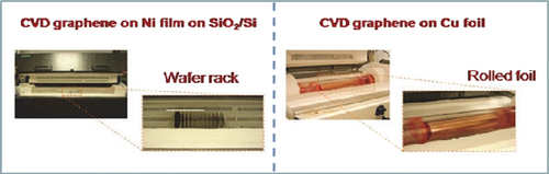
Chemical vapor deposition is a simple, scalable, and cost-efficient method to prepare single- and few-layer graphene films on various substrates; it opens a new route to large-area production of high-quality graphene films for practical applications ().
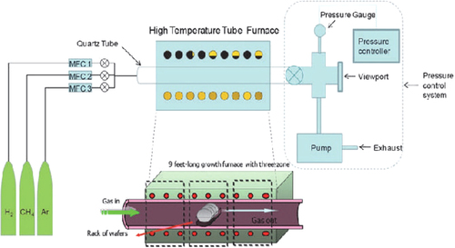
Synthesis of graphene on Ni supported on Si/SiO2 wafers facilitated the breakthrough approach for large-scale graphene production; particularly because Ni films provide an excellent geometrical fit of the ordered graphene/graphite phase of carbon to the crystalline metal surface as well as convenient interactions that favor bond formation between carbon atoms at specific conditions (CitationZhang et al. 2010, CitationEizenberg and Blakely 1979; ).
High temperature-high pressure technique
Graphene has been produced by a high pressure-high temperature (HPHT) growth process from the natural graphitic source material by utilizing the molten Fe–Ni catalysts for dissolution of carbon. The method may lead to a more reliable graphene synthesis and facili- tate its purification and chemical doping (CitationParvizi et al. 2008).
Chemical oxidation of graphite
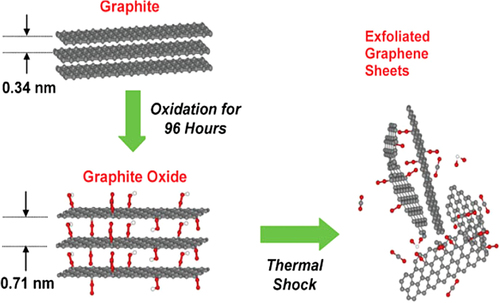
The most popular method employed for the synthesis of graphene is chemical oxidation of graphite (CitationDreyer et al. 2010). This method involves oxidation of graphite to GO using highly oxidizing reagents and subsequently reducing GO to graphene using various reductants (). Chemical oxidation of graphite is an established method using concentrated acids (sulfuric acid, nitric acid, and phosphoric acid) and highly oxidizing agents (potassium permanganate and potassium perchlorate) (CitationMing 2010). Since the 19th century, graphite oxide has been produced by Hummer's method, which typically involves oxidation of graphite in the presence of strong oxidants and acids for extended periods (CitationSu et al. 2009).
Formation of dimanganeseheptoxide from KMnO4 in the presence of strong acid (CitationKoch 1982).
Silicon carbide sublimation
Silicon carbide (6H-SiC) is heated between 1080°C and 1320°C, leading to the growth of graphene. The face of the SiC used for graphene creation, Siterminated or C-terminated, highly influences the thickness, mobility, and carrier density of the graphene (CitationCharrier et al. 2002).
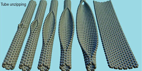
Unfolding CNTs
Graphene ribbons are produced by cutting and unfolding CNTs via chemical etching (KMnO4-H2SO4) or plasma etching. At this scale, the unzipping has been accomplished by harsh acids and the right thermodynamic conditions (CitationBaraton et al. 2011; ).
Figure 5. Modeling illustration of the SWCNT unzipped into monolayer graphene (CitationBaraton et al. 2011).
Applications
Graphene, with its unique combination of physical and electronic properties, is a very promising material not only for electronics, but also for biosensor and bioelectronic applications ().
Transistors
A quantitative understanding of the sensitivity of graphene solution gated field effect transistors (SGFET) capable of operation in aqueous environments is important (CitationFerrari et al. 2006). The transistor conductance can be significantly altered (106 on–off ratio at RT) by a reversible chemical modification (CitationEchtermeyer et al. 2008).
Biomedical applications
In 2008, from the first study on graphene for biomedical applications, much remarkable work has been carried out to explore the use of graphene for widespread biomedical applications, ranging from drug/gene delivery, biological sensing and imaging, antibacterial materials, to biocompatible scaffold for cell culture (CitationGuo and Dong 2011, CitationJiang 2011).
Biofunctionalization with DNA
The large 2D aromatic surface of graphene makes it an ideal substrate for adsorption of certain biomolecules. Importantly, ssDNA can be strongly interfaced onto the graphene surface, the tethering process of ssDNA on graphene is especially on thicker sheets (− 8 nm), and on wrinkled rather than flat surfaces of chemically modified graphene. Patterning ssDNA on graphene layers increases the hole density in the graphene layer in the order of 5.61 × 10¹²/cm2 (CitationMollazade et al. 2013).
Graphene-based FRET biosensors
There is increasing attention toward the use of graphene for the development of FRET biosensors. FRET involves the transfer of energy from a donor fluorophore to an acceptor fluorophore and is one of the advanced tools available for measuring nanometer-scale distance and changes, both in vivo and in vitro (CitationSelvin 2000).
Characterization
XRD theory and concept of interlayer distances of graphene
The principle of XRD for materials is based on Bragg's law, and it is expressed by
where λ is the wavelength of the X-ray, θ is the scattering angle, n is an integer representing the order of the diffraction peak, d is the interplane distance of the lattices, and (hkl) are Miller indices. The XRD peak of the (002) facet of GP gives rise to a critical d002 value as well as the information required for the lattice size and quality (). The GP thickness can be estimated using Sherrer's equation (CitationAhmadi et al. 2014, CitationNejati-Koshki et al. 2013, CitationPourhassan-Moghaddam et al. 2013, CitationMollazade et al. 2013, CitationRezaei-Sadabady et al. 2013, CitationValizadeh et al. 2012, CitationAkbarzadeh et al. 2012a, Citation2012b, Citation2012c, Citation2012d, CitationAkbarzadeh et al. 2013), which is expressed by D002 = Kλ/Bcosθ, where D002 is the thickness of crystallite (here, GP thickness), K is a constant dependent on the crystallite shape (0.89), λ is the X-ray wavelength, B is the full width at half maximum (FWHM), and θ is the scattering angle (CitationTang et al. 2012).
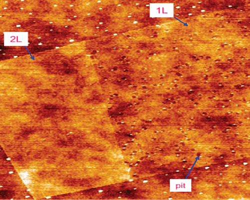
AFM
AFM studies have shown “flat” 10-nm domains of 0.5 nm roughness; other regions can show bowing and bending, with deviation from a hexagonal structure. Graphene is unusually susceptible to a Fermi-level shift because of chemical doping, which can result from edge chemical functionalization in finite-size pieces, and/or from charge transfer by adsorbed or bound species (CitationLiu et al. 2008; ).
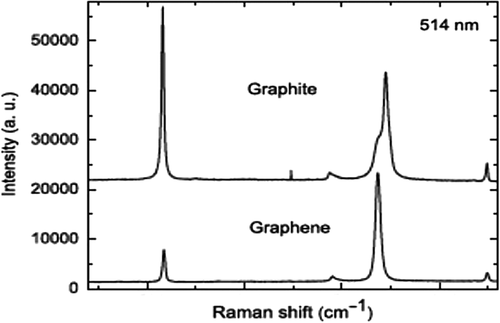
Raman spectra
The Raman spectra of graphene includes the G peak located at 1580 cm− 1 and 2D peak at 2700 cm− 1, caused by the in-plane optical vibration (degenerate zone center E 2 g mode) and second-order zone boundary phonons, respectively. The D peak, located at 1350 cm− 1 due to first-order zone boundary phonons, is absent from defect-free graphene, but exists in defected graphene. Raman spectra could be used to distinguish the “quality” of graphene and to determine the number of layers for n-layer graphene (for n up to 5) by the shape, width, and position of the 2D peak (CitationFerrari et al. 2006; and ).
Authors’ contributions
MK conceived the study and participated in its design and coordination. AA and MM participated in the sequence alignment and drafted the manuscript. EA helped in drafting the manuscript. All authors read and approved the final manuscript.
Acknowledgments
The authors thank the Department of Medical Nanotechnology, Faculty of Advanced Medical Science of Tabriz University, for all the support provided.
Declaration of interest
The authors report no declarations of interest. The authors alone are responsible for the content and writing of the paper.
References
- Ahmadi A, Shirazi H, Pourbagher N, Akbarzadeh A, Omidfar K. 2014. An electrochemical immunosensor for digoxin using core-shell gold coated magnetic nano-particles as labels. Mol Biol Rep. Epub Ahead of Print.
- Akbarzadeh A, Mikaeili H, Zarghami N, Mohammad R, Bsrkhordari A, Davaran S. 2012c. Preparation and in-vitro evaluation of adriamaycin-encapsulated Fe3O4 magnetic nanoparticles modified with biocompatible copolymer. Int J Nanomedicine. 7:1–16.
- Akbarzadeh A, Rezaei-Sadabady R, Davaran S, Joo SW, Zarghami N, Hanifehpour Y, et al. 2013. Liposome: classification, preparation, and applications. Nanoscale Res Lett. 8:102.
- Akbarzadeh A, Samiei M, Davaran S. 2012d. Magnetic nanoparticles: preparation, physical properties, and applications in biomedicine. Nanoscale Res Lett. 7:144.
- Akbarzadeh A, Samiei M, Joo SW, Anzaby M, Hanifehpour Y, Nasrabadi HT, Davaran S. 2012a. Synthesis, characterization and in vitro studies of adriamaycin encapsulated magnetic nanoparticles grafted to smart copolymers on A549 lung cancer cell line. J Nanobiotechnol. 10:46.
- Akbarzadeh A, Zarghami N, Mikaeili H, Asgari D, Goganian AM, Khaksar K, et al. 2012b. Synthesis, characterization and in vitro evaluation of novel polymer-coated magnetic nanoparticles for controlled delivery of adriamaycin. Nanotechnol Sci Appl. 5:1–13.
- Bae S, Kim SJ, Shin D, Ahn JH, Hong BH. 2012. Towards industrial applications of graphene electrodes. Phys Scr. 2012:014024.
- Balandin AA, Ghosh S, Bao W, Calizo I, Teweldebrhan D, Miao F, Lau CN. 2008. Superior thermal conductivity of single-layer graphene. Nano Lett. 8:902–907.
- Baraton L, He Z, Lee CS, Maurice JL, Cojocaru CS, Gourgues-Lorenzon AF, et al. 2011. Synthesis of few-layered graphene by ion implantation of carbon in nickel thin films. Nanotechnology. 22:085601.
- Bolotin KI, Sikes KJ, Jiang Z, Klima M, Fudenberg G, Hone J, et al. 2008. Ultrahigh electron mobility in suspended graphene. Solid State Commun. 146:351–355.
- Charrier A, Coati A, Argunova T. 2002. Solid-state decomposition of silicon carbide for growing ultra-thin heteroepitaxial graphite films. J Appl Phys. 92:2479–2484.
- Chen H, Müller MB, Gilmore KJ, Wallace GG, Li D. 2008. Mechanically strong, electrically conductive, and biocompatible graphene paper. Adv Mater. 20:3557–3561.
- De Arco LG, Zhang Y, Zhou C. 2011. Large Scale Graphene by Chemical Vapor Deposition: Synthesis, Characterization and Applications. 196:162–184.
- Dikin DA, Stankovich S, Zimney EJ, Piner RD, Dommett GH, Evmenenko G, et al. 2007. Preparation and characterization of graphene oxide paper. Nature. 448:457–460.
- Dreyer DR, Park S, Bielawski CW, Ruoff RS. 2010. The chemistry of graphene oxide. Chem Soc Rev. 39:228–240.
- Dreyer DR, Ruoff RS, Bielawski CW. 2010. From conception to realization: an historial account of graphene and some perspectives for its future. Angew Chem Int Ed. 49:9336–9344.
- Echtermeyer TJ, Lemme MC, Baus M, Szafranek BN, Geim AK, Kurz H. 2008. Nonvolatile switching in graphene field-effect devices. IEEE Electron Device Lett. 29:952–954.
- Eda G, Fanchini G, Chhowalla M. 2008. Large-area ultrathin films of reduced graphene oxide as a transparent and flexible electronic material. Nat Nanotechnol. 3:270–274.
- Eizenberg M, Blakely J. 1979. Carbon monolayer phase condensation on Ni (111). Surf Sci. 82:228–236.
- Ferrari A, Meyer JC, Scardaci V, Casiraghi C, Lazzeri M, Mauri F, et al. 2006. Raman spectrum of graphene and graphene layers. Phys Rev Lett. 97:187401.
- Forbeaux I, Themlin J-M, Debever J-M. 1998. Heteroepitaxial graphite on 6H-SiC (0001): Interface formation through conduction-band electronic structure. Phys Rev B. 58:16396.
- Geim AK, Novoselov KS. 2007. The rise of graphene. Nat Mater. 6: 183–191.
- Geim AK. 2009. Graphene: status and prospects. Science. 324: 1530–1534.
- Gilje S, Han S, Wang M, Wang KL, Kaner RB. 2007. A chemical route to graphene for device applications. Nano Lett. 7:3394–3398.
- Gómez-Navarro C, Weitz RT, Bittner AM, Scolari M, Mews A, Burghard M, Kern K. 2007. Electronic transport properties of individual chemically reduced graphene oxide sheets. Nano Lett. 7:3499–3503.
- Guo S, Dong S. 2011. Graphene nanosheet: synthesis, molecular engineering, thin film, hybrids, and energy and analytical applications. Chem Soc Rev. 40:2644–2672.
- Gusynin V, Sharapov S, Carbotte J. 2007. Anomalous absorption line in the magneto-optical response of graphene. Phys Rev Lett. 98:157402.
- Han TH, Lee WJ, Lee DH, Kim JE, Choi EY, Kim SO. 2010. Peptide/graphene hybrid assembly into core/shell nanowires. Adv Mater. 22:2060–2064.
- Huh SH. 2011 Thermal Reduction of Graphene Oxide: Chapter 5. In: Mikhailov S, (ed). Physics and Applications of Graphene - Experiments. InTech.
- Hummers Jr, WS, Offeman RE. 1958. Preparation of graphitic oxide. J Am Chem Soc. 80:1339–1339.
- Jeong H, Jin MH, So KP, Lim SC, Lee YH. 2009. Tailoring the characteristics of graphite oxides by different oxidation times. J Phys D Appl Phys. 42:065418.
- Jiang H. 2011. Chemical preparation of graphene-based nanomaterials and their applications in chemical and biological sensors. Small. 7:2413–2427.
- Kawano Y, Ishibashi K. 2010. A wide-band wavelength-tunable terahertz detector using a graphene transistor. In: IInfrared Millimeter and Terahertz Waves (IRMMW-THz), 2010 35th International Conference. IEEE, 5–10 September, Rome, Italy.
- Kim BH, Kim JY, Jeong SJ, Hwang JO, Lee DH, Shin DO, et al. 2010. Surface energy modification by spin-cast, large-area graphene film for block copolymer lithography. ACS Nano. 4:5464–5470.
- Koch KR. 1982. Oxidation by Mn207: An impressive demonstration of the powerful oxidizing property of dimanganeseheptoxide. J Chem Educ. 59:973.
- Lee C, Wei X, Kysar JW, Hone J. 2008. Measurement of the elastic properties and intrinsic strength of monolayer graphene. Science. 321:385–388.
- Lee DH, Kim JE, Han TH, Hwang JW, Jeon S, Choi SY, et al. 2010. Versatile carbon hybrid films composed of vertical carbon nanotubes grown on mechanically compliant graphene films. Adv Mater. 22:1247–1252.
- Lerf A, He H, Forster M, Klinowski J. 1998. Structure of graphite oxide revisited. J Phys Chem B. 102:4477–4482.
- Li X, Zhang G, Bai X, Sun X, Wang X, Wang E, Dai H. 2008. Highly conducting graphene sheets and Langmuir–Blodgett films. Nat Nanotechnol. 3:538–542.
- Li X, Zhu Y, Cai W, Borysiak M, Han B, Chen D, et al. 2009. Transfer of large-area graphene films for high-performance transparent conductive electrodes. Nano Lett. 9:4359–4363.
- Liang J, Huang Y, Zhang L, Wang Y, Ma Y, Guo T, Chen Y. 2009. Molecular-level dispersion of graphene into poly (vinyl alcohol) and effective reinforcement of their nanocomposites. Adv Funct Mater. 19:2297–2302.
- Liu L, Ryu S, Tomasik MR, Stolyarova E, Jung N, Hybertsen MS, et al. 2008. Graphene oxidation: thickness-dependent etching and strong chemical doping. Nano Lett. 8:1965–1970.
- Ming HN. 2010. Simple room-temperature preparation of high-yield large-area graphene oxide. Int J Nanomed. 6.
- Mollazade M, Nejati-Koshki K, Akbarzadeh A, Hanifehpour Y, Zarghami N, Joo SW. 2013. PAMAM dendrimers arugment inhibitory effect of curcumin on cancer cell proliferation: possible inhibition of telomerase. Asian Pac J Cancer Prev. 14:6925–6928.
- Morozov SV, Novoselov KS, Katsnelson MI, Schedin F, Elias DC, Jaszczak JA, Geim AK. 2008. Giant intrinsic carrier mobilities in graphene and its bilayer. Phys Rev Lett. 100:016602.
- Nejati-Koshki K, Akbarzadeh A, Pourhasan-Moghadam M, Abhari A, Dariushnejad H. 2013. Inhibition of leptinand leptin receptor gene expression by silibinin-curcumin combination. Asian Pac J Cancer Prev. 14:6595–6599.
- Neto AC, Avlund M, Hallatschek O, Nelson DR. 2009. The electronic properties of graphene. Rev Mod Phys. 81:109.
- Niyogi S, Bekyarova E, Itkis ME, McWilliams JL, Hamon MA, Haddon RC. 2006. Solution properties of graphite and graphene. J Am Chem Soc. 128:7720–7721.
- Otsuji T, Watanabe T, El Moutaouakil A, Karasawa H, Komori T, Tsuneyoshi S, et al. 2010. Emission of terahertz radiation from two-dimensional electron systems in semiconductor nano- heterostructures. Comptes Rendus Physique. 11:421–432.
- Park S, An J, Jung I, Piner RD, An SJ, Li X, et al. 2009. Colloidal suspensions of highly reduced graphene oxide in a wide variety of organic solvents. Nano Lett. 9:1593–1597.
- Park S, Ruoff RS. 2009. Chemical methods for the production of graphenes. Nat Nanotechnol. 4:217–224.
- Parvizi R, Teweldebrhan D, Ghosh S, Calizo I, Balandin AA, Zhu H, Abbaschian R. 2008. Properties of graphene produced by the high pressure-high temperature growth process. Micro Nano Lett IET. 3:29–34.
- Patil AJ, Vickery JL, Scott TB, Mann S. 2009. Aqueous stabilization and self-assembly of graphene sheets into layered bio-nanocomposites using DNA. Adv Mater. 21:3159–3164.
- Peres N, Neto AC, Guinea F. 2006. Dirac fermion confinement in graphene. Phys Rev B. 73:241403.
- Pourhassan-Moghaddam M, Rahmati-Yamchi M, Akbarzadeh A, Daraee H, Nejati-Koshki K, Hanifehpour Y, Joo SW. 2013. Protein detection through different platforms of immuno-loop-mediated isothermal amplification. Nanoscale Res Lett. 8:485.
- Rafiee J, Rafiee MA, Yu ZZ, Koratkar N. 2010. Superhydrophobic to superhydrophilic wetting control in graphene films. Adv Mater. 22:2151–2154.
- Ren P-G, Yan DX, Ji X, Chen T, Li ZM. 2011. Temperature dependence of graphene oxide reduced by hydrazine hydrate. Nanotechnology. 22:055705.
- Rezaei-Sadabady R, Zarghami N, Barzegar A, Eidi A, Akbarzadeh A, Rezaei-Tavirani M. 2013. Studies of the relationship between structure and antioxidant activity in interesting systems, including tyrosol, hydroxytyrosol derivatives indicated by quantum chemical calculations. Soft. 2:13–18.
- Rudin S. 2009. Plasma transport in graphene conduction channels and application for the detection of Terahertz signals. In: Semiconductor Device Research Symposium, 2009. ISDRS 9–11 December, College Park, MD.
- Schniepp HC, Li JL, McAllister MJ, Sai H, Herrera-Alonso M, Adamson DH, et al. 2006. Functionalized single graphene sheets derived from splitting graphite oxide. J Phys Chem B. 110:8535–8539.
- Selvin PR. 2000. The renaissance of fluorescence resonance energy transfer. Nat Struct Biol. 7:730–734.
- Sensale-Rodriguez B, Fang T, Yan R, Kelly MM, Jena D, Liu L, Xing H. 2011. Unique prospects for graphene-based terahertz modulators. Appl Phys Lett. 99:113104–113104–3.
- Si Y, Samulski ET. 2008. Synthesis of water soluble graphene. Nano Lett. 8:1679–1682.
- Stankovich S, Dikin DA, Dommett GHB, Kohlhaas KM, Zimney EJ, Stach EA, et al. 2006. Graphene-based composite materials. Nature. 442:282–286.
- Stankovich S, Dikin DA, Piner RD, Kohlhaas KA, Kleinhammes A, Jia Y, et al. 2007. Synthesis of graphene-based nanosheets via chemical reduction of exfoliated graphite oxide. Carbon. 45: 1558–1565.
- Su C-Y, Xu Y, Zhang W, Zhao J, Tang X, Tsai CH, Li LJ. 2009. Electrical and spectroscopic characterizations of ultra-large reduced graphene oxide monolayers. Chem Mater. 21:5674–5680.
- Sun D, Divin CJ, Berger C, de Heer W, Rioux J, Sipe J, Norris TB. 2009. THz emission from coherently controlled photocurrents in epitaxial graphene. In: Lasers and Electro-Optics, 2009 and 2009 International Quantum Electronics Conference. CLEO/QELS, 31 May–5 June, Baltimore, MD.
- Tang Y, Huang F, Zhao W, Liu Z, Wan D. 2012. Synthesis of graphene-supported Li4Ti5O12 nanosheets for high rate battery application. J Mater Chem. 22:11257–11260.
- Valizadeh A, Mikaeili H, Samiei M, Farkhani SM, Zarghami N, Kouhi M, et al. 2012. Quantum dots: synthesis, bioapplications, and toxicitynanoscale. Res Lett. 7:480.
- Viculis LM, Mack JJ, Kaner RB. 2003. A chemical route to carbon nanoscrolls. Science. 299:1361.
- Wang F, Zhang Y, Tian C, Girit C, Zettl A, Crommie M, Shen YR. 2008b. Gate-variable optical transitions in graphene. Science. 320:206–209.
- Wang H, Hao Q, Yang X, Lu L, Wang X. 2010. Effect of graphene oxide on the properties of its composite with polyaniline. ACS Appl Mater. Interfaces. 2:821–828.
- Wang X, Zhi L, Tsao N, Tomović Z, Li J, Müllen K. 2008a. Transparent carbon films as electrodes in organic solar cells. Angew Chem Int Ed Engl. 120:3032–3034.
- Watcharotone S, Dikin DA, Stankovich S, Piner R, Jung I, Dommett GH, et al. 2007. Graphene-silica composite thin films as transparent conductors. Nano Lett. 7:1888–1892.
- Wu Z, Chen Z, Du X, Logan JM, Sippel J, Nikolou M, et al. 2004. Transparent, conductive carbon nanotube films. Science. 305: 1273–1276.
- Yu C, Shi L, Yao Z, Li D, Majumdar A. 2005. Thermal conductance and thermopower of an individual single-wall carbon nanotube. Nano Lett. 5:1842–1846.
- Zhang Y, Gomez L, Ishikawa FN, Madaria A, Ryu K, Wang C, et al. 2010. Comparison of graphene growth on single-crystalline and polycrystalline Ni by chemical vapor deposition. J Phys Chem Lett. 1:3101–3107.
- Zhu Y, Murali S, Cai W, Li X, Suk JW, Potts JR, Ruoff RS. 2010. Graphene and graphene oxide: synthesis, properties, and applications. Adv Mater. 22:3906–3924.