
Abstract
Successive Ionic Layer Adsorption and Reaction (SILAR) was used to deposit nanocrystalline cadmium oxide (CdO) thin films on microscopic glass substrates for various cycles (40–120). This is based on alternate dipping of the substrate in CdCl2 solution made alkaline (pH ∼12) with NaOH, rinsing with distilled water, followed by air treatment with air dryer and annealing at 300 °C for 1 h in air. The prepared films were characterized by X-ray diffraction (XRD), UV–Visible Spectrophotomer (UV–Vis) and Scanning Electron Microscopy (SEM). The 80th cycle was observed to be the saturation stage for this reaction. The XRD results confirmed the films to be CdO with some Cd(OH)2 phase at higher deposition cycles. The films were polycrystalline in nature having high orientation along (1 1 1) and (2 0 0) planes. As the number of cycles increases the calculated average crystallite sizes increase gradually up till the 80th cycle after which a gradual decrease in the crystallite size was observed with increasing number of cycles. The films’ transmittance in the visible and near infrared region decreased as the number of cycles increased and ranged between 25 and 80%. This work shows the feasibility of using simple SILAR method at room temperature to obtain Cd(OH)2 films which are transformed to CdO thin films after annealing.
1 Introduction
Thin films that are simultaneously transparent to visible light and electrically conducting have been widely studied because of their wide range of applications (Zhu et al., Citation2013; Chu and Chu, Citation1990; Jefferson et al., Citation2008; Murthy and Rao, Citation1999"). Oxide films of cadmium, indium, as well as tin, in period five of the periodic table have been shown to have high transmittance in the visible and near infrared regions and high electrical conductivity (Murthy and Rao, Citation1999; Eze, Citation1998; Varkey, Citation1994; Dou, Citation1998; Elttaye et al., Citation2013"). These properties have made them good candidates for use as transparent conducting oxide (TCO), but of these three metals, oxide of cadmium appears to be least used. Cadmium oxide is a degenerate, n-type semiconductor with a wide energy band gap of about 2.16–2.42 eV at room temperature (Chu and Chu, Citation1990; Jefferson et al., Citation2008; Murthy and Rao, Citation1999; Eze, Citation1998"). CdO is used as a transparent conductive material and this transparent conducting property of CdO was first presented by Badeker in 1907 (Eze, Citation1998; Varkey, Citation1994; Dou, Citation1998"). The high conductivity exhibited by CdO results from the presence of anion vacancies or through doping (CitationChu and Chu, 1990) and it crystallizes in the sodium chloride (FCC) structure (CitationOrtega et al., 1999). CdO properties such as large band-gap, low electrical resistivity and high transmittance in the visible region make it useful for a plethora of applications such as photodiodes, phototransistors, photovoltaic cells, transparent electrodes, liquid crystal displays, IR detectors, and anti reflection coatings (Murthy and Rao, Citation1999; Eze, Citation1998; Lokhande, Citation2004; Ellis and Irvine, Citation2004; Baranov et al., Citation1997; Gupta et al., Citation2011"). The properties of CdO films can be optimized to a suitable parameter value in order to suit a particular application by controlling some of the process parameters like film thickness, concentration of solution, temperature of the substrate and the solution flow rate etc. (Varkey, Citation1994; Dou, Citation1998; Ortega et al., Citation1999; Lokhande, Citation2004; Ellis and Irvine, Citation2004; Baranov et al., Citation1997").
Figure 4 Plot of absorbance against wavelength of CdO thin films deposited on microscope glass slide at three different deposition cycles.
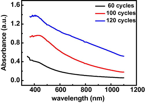
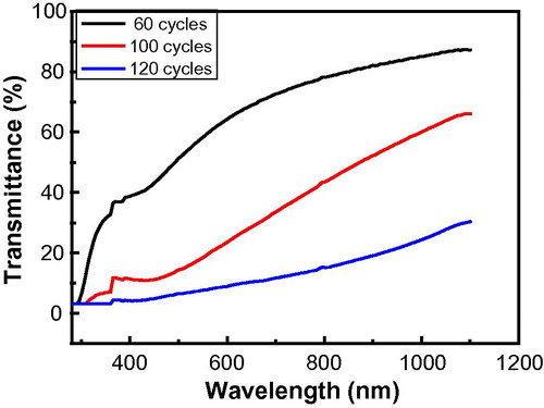
Figure 5 Plot of transmittance against wavelength of CdO thin films deposited on microscope glass slide at three different deposition cycles.
Many methods have been used to synthesize CdO for various applications. Such methods include but not limited to ion beam sputtering (CitationChu and Chu, 1990), magnetron sputtering (Baranov et al., Citation1997; Gurumurugan et al., Citation1996; Subramanyam et al., Citation1997",) spray pyrolysis (Murthy and Rao, Citation1999; Ismail, Citation2009; Mishra et al., Citation2009"), reactive pulsed laser deposition technique (CitationIsmail et al., 2007) thermal deposition (Eze, Citation1998; Suhail et al., Citation2012"), metal organic chemical vapor deposition (CitationEllis and Irvine, 2004), chemical bath deposition (de León-Gutiérreza et al., Citation2006; Khallaf et al., Citation2011; Al-Jawad and Alogili, Citation2009"), SILAR (Salunkhe and Lokhande, Citation2008, Gokul et al., Citation2013; Balu et al., Citation2012") etc.
Of all these methods, SILAR seems to be one of the less frequently used methods in the literature for CdO deposition. SILAR means ‘Successive Ionic Layer Adsorption and Reaction’ and is also known as a modified version of chemical bath deposition technique. It is one of the suitable chemical methods used for the formation of metal oxides in which the thin films are obtained by immersing a substrate into separately placed cationic and anionic precursor solutions (CitationPathan and Lokhande, 2004). This method is capable of producing metal oxide films at relatively low temperature and is relatively simple. It does not require expensive equipment, and there is minimal waste of chemicals when compared with other methods. Other advantages of SILAR are not limited to the fact the deposition rate and the thickness of the required film can be easily controlled over a wide range by changing the deposition cycle; and there are no restrictions on the substrate material, dimensions or surface profile to be used. Unlike power methods, for example, the frequency magnetron sputtering, SILAR does not cause local over heating that may be detrimental to the deposited material and it does not require vacuum at any stage compared to the vapor deposition methods (CitationBalu et al., 2012). However, the major disadvantage of SILAR is that for oxide films, the hydroxide phase is formed first which is then converted to the oxide on annealing. Noteworthy, this limitation is not peculiar to SILAR but is observed in other solution growth methods.
In this work, SILAR method was used to deposit thin films of CdO on microscopic glass substrates after various cycles (40–120) using CdCl2 as the Cd2+ ion source. The deposited films were characterized structurally, morphologically and optically. The effects of various cycles on the properties of the films were studied and their respective possible applications based on these properties were presented.
2 Experimental details
Glass slides were degreased in concentrated tetraoxosulphate (VI) acid (H2SO4), washed with detergent and distilled water, ultrasonicated in a mixture of acetone and double distilled water for 10 min and then dried in an oven. Cadmium oxide thin films were deposited onto the cleaned glass substrates by alternate immersion of the glass substrate in CdCl2 (Cd2+ ion source) and in double distilled water (OH- source) at room temperature. CdCl2 and H2O served as the cationic and anionic solutions respectively. The alkalinity of cadmium chloride solution was increased to pH ∼12 with the addition of sodium hydroxide. As the cleaned glass substrate was immersed in the alkaline cadmium chloride solution, cadmium complex adsorbed on the substrate. The glass substrate with the cadmium complex is then immersed in distilled water and the reaction occurred on the glass surface to form Cd(OH)2. The period of dipping the substrate in the cadmium bath was referred as “adsorption” and that in H2O as “reaction”. This process forms one cycle and was repeated severally (40–120) in order to increase the film thickness. After each cycle, the glass slide was rinsed with distilled water and after a complete cycle the films were dried with an air dryer. Finally, the deposited films were annealed in air at 300 °C for 1h to transform the hydroxide phase to the oxide.
2.1 Characterizations
The elemental composition of the samples was determined by X-ray Energy Dispersion spectroscopy (EDX) with accelerating voltage of 10 kV while phase identification was performed by means of X-ray diffraction (XRD) using a XPERT-PRO diffractometer with CuKα radiation on an operating voltage of 40 kV and current of 40 mA. The morphology and the crystal sizes were investigated with the aid of Scanning Electron Microscope SEM (model S-4700, HITACHI) operating at an acceleration voltage of 10 kV. The optical properties of the films were examined by using a UV–Visible spectrophotometer at normal incident of light in the wavelength range of 200–1100 nm. The band-gaps and the refractive index of the samples were calculated from the absorption spectra.
3 Results and discussions
3.1 Thin film formation
Dipping the glass slides in the beaker containing cadmium chloride and excess sodium hydroxide solution for 30 s causes a cadmium complex ion to adsorb on the substrate due to attractive forces between ions in the solution and that on the glass. The cadmium complex ions can be represented with the following equations:
The glass substrate with the adsorbed cadmium sodium oxide ion is immersed into a beaker of distilled water and the ion is converted into cadmium hydroxide. Sodium ion in the complex is attracted to the hydroxide ion to form sodium hydroxide while the CdO2− in the complex is attracted to the H+ to form the cadmium hydroxide ion.
On annealing at a temperature of 300 °C the cadmium hydroxide transforms into the oxide phase. The deposited films showed good adherence to the substrate after annealing.
3.2 Energy dispersion spectroscopy (EDX)
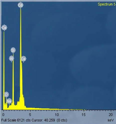
shows the EDX spectrum of the deposited films. The EDX spectrum shows the characteristic X-ray energy level of Cadmium (Kα = 3.133 KeV and Kβ = 3 keV) and oxygen (Kα = 0.523 KeV). Other elements present such as silicon, calcium and aluminum, are from the glass substrate while sodium is from the precursors used.
Figure 1 EDX spectrum of the deposited film.
3.3 X- Ray diffraction
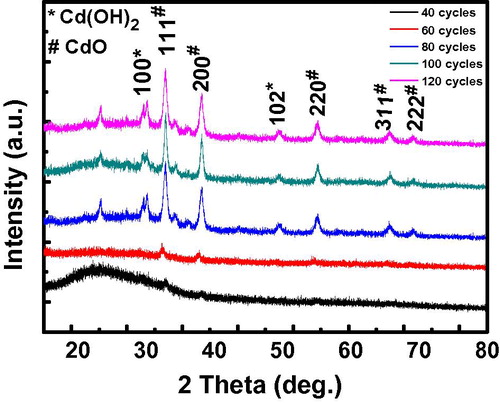
The XRD patterns of the deposited CdO films are shown in . The several peaks observed in all the diffractograms confirm the polycrystalline nature of the CdO films deposited. The prominent peaks observed in the diffraction pattern are due to diffraction from (1 1 1), (2 0 0), and (2 2 0) cubic phase formation as compared with standard X-ray diffraction data file JCPDS (file No. 75-0594). The peaks observed at 2θ = 29.6° and 49.5° corresponds, respectively, to the diffraction from (1 0 0) to (1 0 2) crystal planes of the hexagonal polycrystalline phase of Cd(OH)2 as confirmed from the ASTM card. This, therefore, implied that all the formed Cd(OH)2 were not transformed into CdO. However, these peaks are observed only for the 80–120 cycles implying that as the cycles increased, the rate of transformation of Cd(OH)2 to CdO is reduced. Hence, these higher cycle films need to be annealed at a temperature higher than 300 °C or for a longer time so that all the hydroxide phase can be transformed to the oxide. The 40 cycle film showed only (1 1 1) and (2 0 0) diffraction peak and it is observed that the number of peaks increased and became more defined as the number of cycles increased up to 80 cycles. This shows increase in the crystallinity and crystal size of the films. A slight decrease in peak intensity for 100 and 120 cycles compared to the 80 cycle film was observed. In thin film deposition by the SILAR method, there is a stage of saturation after which further cycles initiate no further reaction and/or the already deposited film begins to peel. This peeling disorients the crystals’ structure and this explains the difference in the peak intensity. Hence the 80th cycle seems to be that saturation stage for this reaction.
Figure 2 XRD patterns of CdO thin films prepared via SILAR method microscope glass slide at various deposition cycles.
The crystallite sizes were estimated using Scherrer relation,(1) Where K is a constant taken to be 0.9, λ is the wavelength, θ is the Bragg’s angle and β is full width half maximum (FWHM) of the preferential plane. The dislocation density (δ), defined as the length of dislocation lines per unit volume, has been estimated using the equation (CitationBilgin et al., 2005):
(2) Where δ is the measure of the amount of defects in a crystal.
shows the comparison of the observed d values obtained for various cycles with the standard values as well as the estimated grain sizes.
Table 1 Comparison of d values (Å) and hkl plane for the CdO films.
It can be seen from that the highest average crystallite size occurred in the film deposited at the 80th cycle. On the other hand, the obtained lesser values of δ (3.36 × 10¹⁶ and 4.93 × 10¹⁶ lines/m2) for the films formed after 40 and 60 cycles respectively indicate that the degree of crystallization is higher for these films. This is in comparison with the values obtained for 80, 100 and 120 cycles which are (8.43, 15.70, and 6.55) × 1016 lines/m2 respectively.
3.4 Scanning Electron Micrography
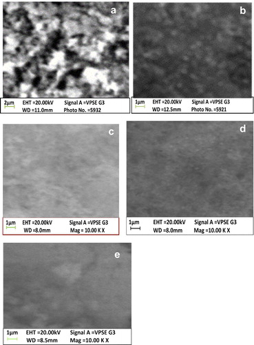
The three-dimensional surface morphological study of the CdO films for different cycles was carried out using SEM images as shown in . From the micrographs, it is evident that the samples are composed of the nanocrystalline grains along with some spongy clusters. The spongy cluster reduces as the number of cycle increases. It is observed that the Cd(OH)2/CdO films cover the whole length of the substrate used.
Figure 3 SEM micrographs of CdO thin films deposited on microscope glass after (a) 40 cycles (b) 60 cycles (c) 80 cycles (d) 100 cycles and (e) 120 cycles.
3.5 Optical studies
and show the absorbance and the transmittance spectrum respectively for the films. It is observed that the absorbance decreases gradually with increase in wavelength and as the number of cycles increased. The increased absorbance by the higher cycles is due to increase in the thickness. The thickness was estimated from the optical result using Eq. Equation(3)(3) :
(3) Where
T is the transmittance (0–1),
R is the reflectance
A = absorbance of the film,
α(λ) = absorption coefficient in (cm−1) and
d = thickness in (cm).
The presence of absorption edge (between 415–425 nm) indicates that the films have a good degree of crystallinity (Al-Hussam and Jassim, Citation2012; Balu et al., Citation2012"). The maximum transmittance in the wavelength range of 350–110 nm was found to be 87, 66, and 30 for 60, 100, and 120 cycles respectively. The lower cycle films could be used for optical coatings for solar cells as they exhibit high transparency.
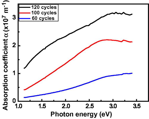
The dependence of absorption coefficient α on the photon energy is shown in . The values were obtained by using the relation:(4) Where T is the transmission and d is the thickness of the film. The absorption coefficient exhibits high values in the short wavelength region and this implies that there is a high probability of the transition being a direct allowed one (CitationSuhail et al., 2012). This means that the conduction band minimum and the valence band maximum occur at the same value of crystal momentum and the transition is caused only by a photon.
Figure 6 Variation in absorbtion coefficient with photon energy, (hν) for CdO thin films deposited via SILAR method at three different deposition cycles.
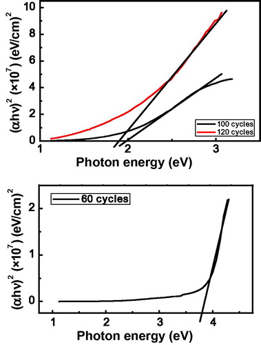
The optical energy band gap value (Eg) for the deposited CdO films was determined by using Tauc’s equation:(5) Where A is a constant, hν is the photon energy and α is the absorption coefficient, while n depends on the nature of the transition. For direct transitions n = ½ or ⅔, while for indirect ones n = 2 or 3, depending on whether they are allowed or forbidden respectively. It is found that the relation for n = ½ yields linear dependence, which describes the allowed direct transition. Eg is then determined by the extrapolation of the portion at (α = 0) as shown in . The values of 3.81 eV, 2.0 eV and 1.85 eV were estimated for the 60, 100, and 120 cycles respectively. Particles whose dimensions become comparable to the bulk exciton Bohr radius are observed to exhibit strong quantum confinement effect, which result in increase in the band gap with decreasing particle size (CitationAl-Hussam and Jassim, 2012). However, the bulk exciton Bohr radius of CdO is not available in the literature and it is therefore difficult to conclude as to which confinement regime the CdO nanocrystals belong (CitationGhosh and Rao, 2004). Hence, the CdO films may not obey the quantum confinement effect.
Figure 7 Plot of (αhν)2 vs. photon energy (hν) for CdO thin films showing the direct band gap at 3.81 eV (60 cycles), 2.0 eV (100 cycles) and 1.85 eV (120 cycles).
The obtained bandgap values for the higher cycles were slightly lower than what has been reported using SILAR method. For instance, CitationBalu et al. (2012) and CitationBeevi et al. (2010) while varying the concentration of the precursor obtained values in the range of 2.27–2.48 eV and 2.54–2.58 eV respectively. CitationMishra et al. (2009) obtained 2.37 eV using spray pyrolysis while CitationKhallaf et al. (2011) obtained 2.53 eV using chemical bath deposition method. The lower values could be attributed to the presence of Cd(OH)2 in the higher cycle films.
4 Conclusion
Transparent CdO thin films were fabricated by the cost effective SILAR method. XRD studies show that all the films are polycrystalline in nature with cubic structure having preferential orientation along (1 1 1) and (2 0 0) plane. The calculated average grain sizes increased between the 40 and 80 cycles and decreased gradually after the 80th cycle. Cd(OH)2 phase was detected at higher cycles hence these higher cycle films need to be annealed at a higher temperature(above 300 °C) in order to transform all the hydroxide to oxide. The maximum transmittance in the wavelength range of 350–110 nm was found to be 87, 66 and 30 for 60, 100 and 120 cycles respectively. The range of optical band gap estimated for various cycles of the CdO films is between 1.85 and 3.81 eV. The films were found to exhibit very promising physical properties which make them desirable for optical coating as well as other opto-electronic applications.
Notes
Peer review under responsibility of University of Bahrain.
Related Research Data
References
- A.M.A.Al-HussamS.A.-J.JassimSynthesis, structure, and optical properties of CdS thin films nanoparticles prepared by chemical bath techniqueJ. Assoc. Arab Univ. Basic Appl. Sci.1120122731
- S.M.H.Al-JawadH.K.J.AlogiliGrowth kinetics of chemically deposited CdO thin filmsEng. Tech. J.2711200923352344
- A.R.BaluV.S.NagarethinamM.SuganyaN.ArunkumarG.SelvanEffect of the solution concentration on the structural, optical and electrical properties of SILAR deposited CdO thin filmsJ. Electron Devices122012739749
- A.M.BaranovY.U.MalovS.A.TeryoshimV.O.ValdnerInvestigation of the properties of CdO filmsTech. Phys. Lett.23101997805806
- M.M.BeeviM.AnusuyaV.SaravananCharacterization of CdO thin films prepared by SILAR deposition techniqueInt. J. Chem. Eng. Appl.122010151154
- V.BilginS.KoseF.AtayI.AkyuzThe effect of substrate temperature on the structural and some physical properties of ultrasonically sprayed CdS filmsMater. Chem. Phys.942005103108
- T.L.ChuS.S.ChuDegenerate cadmium dioxide films for electronic devicesJ. Electron. Mater.199199010031005
- L.R.de León-GutiérrezaJ.J.Cayente-RomeroaJ.M.Peza-TapiaaE.Barrera-CalvaJ.C.Martínez-FloresM.Ortega-LópezSome physical properties of Sn-doped CdO thin films prepared by chemical bath depositionMater. Lett.60200638663870
- Y.DouN-type doping in CdO ceramics: a study by EELS and photoemission spectroscopySurf. Sci.3981998241258
- D.M.EllisJ.C.IrvineMOCVD of highly conductive CdO thin filmsJ. Mater. Sci.: Mater. Electron.152004369372
- A.-H.K.ElttayeH.M.AjeelA.I.KhudiarEffect of annealing temperature and doping with Cu on physical properties of cadmium oxide thin filmsJ. Mater. Res. Technol.222013182187
- F.C.EzeCdO thin films synthesized by a modified reactive thermal deposition processII Nuovo Cimento20D9199814211430
- M.GhoshC.N.R.RaoChem. Phys. Lett.3934–62004493497
- B.GokulP.MatheswaranR.SathyamoorthyInfluence of annealing on physical properties of CdO thin films prepared by SILAR methodJ. Mater. Sci. Technol.29120131721
- R.K.GuptaK.GhoshR.PatelP.K.KaholBandgap engineering of rare earth element doped nanostructured cadmium oxide thin filmsPhysica E4412011163167
- K.GurumuruganD.MangalarajA.S.K.NarayandassMagnetron sputtered transparent conducting CdO thin filmsJ. Electron. Mater.2551996765770
- R.A.IsmailB.G.RasheedE.T.SalamM.Al-HardyHigh transmittance–low resistivity cadmium oxide films grown by reactive pulsed laser depositionJ. Mater. Sci.: Mater. Electron.18200710271030
- R.A.IsmailImproved characteristics of sprayed CdO films by rapid thermal annealingJ. Mater. Sci.: Mater. Electron.2012200912191224
- P.H.JeffersonS.A.HatfieldT.D.VealK.P.DavidC.F.McConvilleJ.Zúñiga-PérezV.Muñoz-SanjoséBandgap and effective mass of epitaxial cadmium oxideAppl. Phys. Lett.9222008022101022103
- H.KhallafC.-T.ChenL.-B.ChangO.LupanA.DuttaH.HeinrichA.ShenoudaL.ChowInvestigation of chemical bath deposition of CdO thin films using three different complexing agentsAppl. Surf. Sci.257201192379242
- B.LokhandeStudies on cadmium oxide sprayed thin films deposited through non-aqueous mediumMater. Chem. Phys.842–32004238242
- R.L.MishraA.K.SharmaS.G.PrakashGas sensitivity and characterization of cadmium oxide (CdO) semi conducting thin film deposited by spray pyrolysis techniqueDig. J. Nanomater. Biostruct.432009511518
- L.C.S.MurthyK.S.R.K.RaoThickness dependent electrical properties of CdO films prepared by spray pyrolysis methodBull. Mater. Sci.2261999953957
- M.OrtegaG.SantanaA.Morales-AcevedoOptoelectronic properties of CdO–Si heterojunctionsSuperficies y Vacío91999294295
- H.M.PathanC.D.LokhandeDeposition of metal chalcogenide thin films by successive ionic layer adsorption and reaction (SILAR) methodBull. Mater. Sci.272200485111
- R.R.SalunkheC.D.LokhandeEffect of film thickness on liquefied petroleum gas (LPG) sensing properties of SILAR deposited CdO thin filmsSens. Actuators, B12912008345351
- T.K.SubramanyamB.R.KrishnaS.UthannaB.S.NaiduP.J.ReddyPhysical investigations on d.c. magnetron reactive sputtered cadmium oxide filmsJ. Mater. Sci. Lett.16199715761579
- M.H.SuhailI.S.IbrahimG.M.RaoCharacterization and gas sensitivity of cadmium oxide thin films prepared by thermal evaporation techniqueJ. Electron Devices132012965974
- A.VarkeyTransparent conducting cadmium oxide thin films prepared by a solution growth techniqueThin Solid Films23921994211213
- Y.ZhuR.J.MendelsbergJ.ZhuJ.HanA.AndersTransparent and conductive indium doped cadmium oxide thin films prepared by pulsed filtered cathodic arc depositionAppl. Surf. Sci.2652013738744