
 ?Mathematical formulae have been encoded as MathML and are displayed in this HTML version using MathJax in order to improve their display. Uncheck the box to turn MathJax off. This feature requires Javascript. Click on a formula to zoom.
Abstract
Silicon carbide (SiC) MOSFETS are increasingly favoured in power electronics for their improved properties compared to silicon-based counterparts, such as IGBTs. Their ability to operate at higher switching frequencies and execute faster switching transients is notable. However, these features also raise significant concerns with electromagnetic interference (EMI). To exploit the full capabilities of SiC-based technology, meticulous design strategies encompassing the power stage, commutation loop, and gate drive are essential. This paper conducts a comprehensive review of existing gate drive techniques aimed at enhancing the performance of SiC devices. Moreover, this study introduces an innovative approach for optimizing switching processes through the use of active gate drivers (AGD). By pre-mapping the gate-source voltage profiles for different conditions (such as load current, temperature, and DC-link voltage), it is possible to achieve a significantly improved switching trajectory. This optimization process can be applied on a cycle-by-cycle basis in practical scenarios. Herein, pre-mapping and optimization have been experimentally confirmed in a half-bridge configuration. Through simulation, it is demonstrated that optimizing the switching trajectory can lead to a balanced compromise between EMI and switching losses, showcasing the potential for significant performance enhancements in SiC device operation.
1. Introduction
Elevating the performance and efficiency of power electronics, silicon carbide (SiC) power transistors have emerged as pivotal elements in the field's development. Their impact is pronounced, with SiC semiconductors being integrally used in industries such as automotive, energy, and manufacturing. The advantages of SiC technology, including fast switching speeds and reduced channel resistance, contribute to enhanced efficiency, reduced heatsink requirements, superior dynamic performance, and the facilitation of innovative applications.
Performance improvements from Silicon devices stem from enhanced material properties. However, regardless of the topology used, fast switching which characterizes SiC power transistors causes multiple challenges in the application, namely the need for improved filtering of electromagnetic interference (EMI), careful commutation loop design, and improved gate drive.
Adjusting the gate resistance or applying the appropriate voltage waveform to the MOSFET gate can mitigate EMI and switching losses [Citation1]. Recent studies have also explored passive techniques for optimizing these parameters [Citation2]. The design of the gate drive stage is crucial in power electronics, particularly with active gate drives, due to its significant impact on system performance.
This paper is an extension of [Citation3], and is organized as follows: Section 2 covers an overview of a switching model for a hard-switched SiC half-bridge. Next, Section 3 covers a basic overview of switching influence on EMI, with a focus on conducted emissions of a half-bridge. In Section 4 a comparative analysis of advanced gate drivers is shown. Section 5 covers the switching optimization, direct and inverted maps for an active gate driver. Section 6 showcases experimental verification of the concept, while Section 7 simulates the optimized active switching strategy for a three-phase inverter. Finally, a conclusion and result summary is given in Section 8.
2. SiC MOSFET hard-switching model
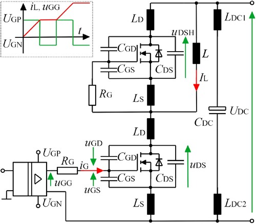
The most used building block of modern power electronics converters is a two-quadrant half-bridge. Its model is depicted in Figure , showing well documented parasitic elements, which will be discussed further on. To design an appropriate gate drive for the SiC MOSFET, it is required to study the basic model of the SiC MOSFET switching in a half-bridge configuration.
Figure 1. Half-bridge with parasitic elements in the commutation loop.
2.1. Half-bridge parasitic elements and switching process
The basic building elements of a half-bridge are a transistor pair and a DC-link capacitor. However, additional parasitic elements appear due to the layout of individual connecting elements, printed circuit board (PCB) or module segments, and component internals.
Identifying parasitic elements in the switching loop necessitates analysing inductances from filter capacitors, connecting buses, and transistor terminals. The total parasitic inductance, , is the sum of all inductances in the commutation loop (single transistor + DC-link). The inductance of the source is especially important as it reduces switching speed and affects voltage overshoots. Lower voltage overshoots enable the transistors to operate at higher voltages, improving the utilization of SiC MOSFETs and power densities of converters [Citation4, Citation5]. In addition to the commutation loop inductance, the parasitic capacitance to the heatsink and the internal parasitic capacitances of the MOSFET need to be considered. The parasitic capacitances of MOSFETs are highly non-linear and greatly affect the switching. They are labelled as
and
. The gate voltage at which the channel current is just barely supported is defined as:
(1)
(1) Here
and
are plateau and threshold voltages respectively. The plateau voltage is channel current dependent and for a given load current (
),
is lower for turn-off and higher for turn-on due to displacement currents flowing through MOSFET parasitic capacitances [Citation6]. Because of this, the plateau voltage is often numerically solved. However, most studies often use an approximation and use the load current (
) as the channel current. Transconductance (
), is defined as the slope of the MOSFET transfer characteristics in an ohmic region at a specific operating point:
. The resonant circuit formed by parasitic capacitances and inductances often leads to ringing at the switching transition's conclusion [Citation4]. For symmetrical high-side and low-side transistors, the ringing frequency is determined by the RLC circuit of the switching loop and one transistor's parasitic capacitance, given by:
(2)
(2) Lowering parasitic inductance reduces the energy in parasitics, thereby diminishing EMI. Yet, it's shown that the majority of converter noise stems from the switch's current and voltage changes.
2.2. Switching model
The model, applicable to many topologies, describes the low-side MOSFET during turn-on and turn-off in a typical double-pulse test setup where an inductive load is connected across the high-side MOSFET [Citation7]. It is assumed that the high-side transistor has been just turned off and its body diode continues to conduct the load current. In addition, it is assumed that the load current () is constant during the complete low-side impulse duration, i.e. turn-on and turn-off period. The mathematical model which defines the current-voltage relations of the MOSFET in the switching process is shown in Figure , with governing equations in Table .
Table 1. System equations for half bridge in Figure .
Here is the total (external and internal) resistance of the gate. For simplicity, most of the non-dominant inductive parasitic elements are omitted from the model. The parasitic inductance of the source (
) causes most of the oscillations and overshoots, while the parasitic inductance on the gate (
) for a conventional gate driver (CGD) typically does not cause voltage oscillations if designed properly.
Turn-on and turn-off both have distinct subintervals, i.e. stages , as also depicted in Figure (a,b), respectively. The following is a model for MOSFET switching with asymmetric gate supply. Turn-on starts with a rising edge of a gate drive
from
to
.
Figure 2. (a) Theoretical turn-on waveforms of with subintervals (1) to (4) and (b) theoretical turn-off waveforms for subintervals (5) to (8) showing drain-source voltage, drain current, gate-source voltage and gate current with corresponding interval durations. Current and voltage overshoots caused by reverse recovery current and parasitic inductances are shown but omitted from the model.
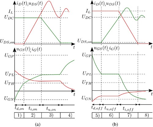
2.2.1. Turn-on delay
After the turn-on voltage is asserted, a delay takes place until the voltage rises to the and the MOSFET starts to overtake the current of its counterpart. Since the drain-source voltage
does not change, the parasitic capacitance
can be viewed as a short circuit. Neglecting all parasitic inductances and the stated conditions, the solutions of the equations are:
(8)
(8)
(9)
(9) At the same time,
, and the observed transistor current is still
. For a complex model, in which
is included, the gate voltage follows the envelope defined by (Equation9
(9)
(9) ), while any gate-source inductance causes high-frequency oscillations.
2.2.2. Current rise time
This subinterval starts when , and ends when
is valid. This coincides with drain current
rising to load current
. The transistor current takes over the complementary transistor's body diode current. The MOSFET is in the saturation region, and the channel current is determined by the transconductance while
is valid. If the drain inductance is ignored, the gate voltage continues to rise with the same conditions as before.
(10)
(10)
(11)
(11)
(12)
(12) Here
holds. Equation (Equation12
(12)
(12) ), i.e. channel current expression, follows from (7) if source parasitic inductance is ignored. The remaining loop inductances cause the drain-source voltage drop (
) if present or not ignored. The
displacement current is zero if its voltage is unchanged (when
). Due to the symmetry of the components, the current gradient (
) is equal to the current gradient of the opposing intrinsic diode [Citation8]. A drain current overshoot due to reverse recovery is observed during this time if applicable.
2.2.3. Voltage fall time
Voltage fall starts when becomes equal to the load current, and when
. It ends when
falls to the ohmic voltage drop in conduction (
). In this sub-interval, parasitic capacitances determine the voltage gradients. Due to the Miller effect,
for this subinterval appears to be very large, so both the gate-source voltage
and the gate current
are constant. The gate current drains the charge from the Miller capacitance
. From the Equation (4) and previous considerations:
(13)
(13)
(14)
(14) Because of high
sensitivity to
, this capacitor's value must be approximated as the mean of voltage-dependent capacitance
, as in [Citation9].
(15)
(15) The effects of displacement currents flowing through both opposite
and
and observed transistor
can be included in the model by utilizing (7), however, often
holds, so the influence of this effect can be neglected for turn-on transition.
Due to the symmetry of low and high-side transistors, their drain-source voltage gradients are equal but of opposite signs.
(16)
(16) Here it should be also noted that for CGD turn-on
decreases linearly with increasing load current
due to Miller plateau voltage shifting up.
2.2.4. Gate voltage rise time
The gate voltage must rise to the terminal voltage , so the voltage and current curves continue from their previous values. The Miller capacitance
is charged to the gate voltage, and no longer appears very large from driver side. The voltage
is stabilized at the value
, while the current is stabilized at the value of the load current
.
(17)
(17)
(18)
(18) MOSFET turn-off can be viewed as the four previously mentioned time intervals in reverse order. The current-voltage relationships shown in (3)–(7) can still be applied.
2.2.5. Turn-off delay
Starts with the turn-off voltage () appearing at the output stage of the gate drive, and lasts until the gate-source voltage drops to the plateau voltage (
):
(19)
(19)
(20)
(20) During this subinterval,
holds true, and the observed transistor current is still
.
2.2.6. Voltage rise time
In this subinterval, the voltages of the commutation loop change with the Miller effect. Analogous to the voltage fall time interval, for a large enough current, the following applies: (21)
(21)
(22)
(22) However, this voltage gradient model is valid for load currents above a transistor-specific kink current
[Citation2], where voltage rise time becomes less dependent on load current. On the contrary, for currents lower than
, the sum of currents in (7) are such that
, and all of the load current
distributes to charge all of the parasitic capacitances. This type of switching is essentially lossless and typically called ZVS in literature [Citation2, Citation9].
(23)
(23) For load currents larger than
during turn-off, the portion of load current is flowing to the channel as well, instead of only charging both
capacitances. Therefore, using (7), boundary condition is when
, and
can be found as:
(24)
(24) It should also be noted that, analogous to
, a charge-equivalent capacitance using (Equation15
(15)
(15) ) needs to be calculated for
.
2.2.7. Current fall time
Starts when and is valid until
, that is, until the drain current
drops to
. The MOSFET is in the saturation region.
(25)
(25)
(26)
(26)
(27)
(27) If stray inductances are not ignored, an overshoot is seen on drain-source voltage
.
2.2.8. Gate voltage fall time
The gate voltage must drop to the terminal voltage , continuing with the current-voltage relations of the previous interval, with the current
.
(28)
(28)
(29)
(29)
Therefore it is possible to calculate the approximate current and voltage rise and fall times during turn-on and turn-off (according to [Citation10]) and from this follows the Table in which . From these results, it is possible to estimate the losses and EMI of the converter.
3. Fundamental EMI analysis for a half-bridge
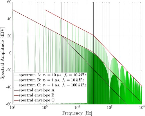
According to the considerations from the previous chapter, it is possible to achieve switching gradients of up to . However, the high switching speed increases EMI. From a practical standpoint, EMI generated by power converters is divided into conducted emissions, transmitted by a conductor leads and radiated emissions, transmitted to the surrounding space.
Table 2. Approximate duration of SiC MOSFET switching subintervals.
Conducted EMI can be further divided into differential mode (DM) and common mode (CM) interference [Citation11].
DM noise pair appears on both of the bus lines of the DC-link in counter-phase (
and
CM noise appears in-phase in both bus lines (
Because power electronics converters are inherently pulsed devices, certain parts of the commutation loop (mainly the switch node) have pulsed currents and voltages with finite rise and fall times. Therefore, it is important to analyse the spectrum resulting from the trapezoidal waveform. Using Fourier transform of a trapezoidal waveform with amplitude A, rise time and duty cycle
, magnitude and phase of nth harmonic are obtained (Equation37
(37)
(37) ), with switching frequency,
, being the fundamental harmonic [Citation12]:
(37)
(37) It is assumed that the voltage rise time is equal to the fall time. By taking the envelope of the spectrum, i.e. taking the absolute value, converting to decibels and using the limiting value of
, it can be seen that the cutoff frequencies above which
term is active are:
(38)
(38)
(39)
(39) By shortening the rise time, the term with
shifts the second cutoff frequency higher, resulting in an increase of
for a band above
, as observed in Figure .
According to the above consideration, the linear dependence of the noise bandwidth on rise and fall times is visible. Furthermore, this implies a possible trade-off between switching losses and the permissible EMI by the relevant standards [Citation1].
Figure 3. Spectrum of a trapezoidal voltage with and
as parameters, and signal amplitude
with cutoff frequencies
and
highlighted.
4. Comparative analysis of advanced gate drivers
4.1. Gate drivers for SiC MOSFETs
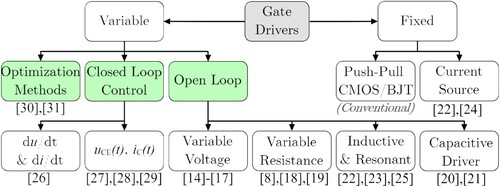
Gate drivers for SiC MOSFETs mostly use an isolated DC/DC converter as an asymmetric voltage source and are driven with CMOS or bipolar push-pull outputs to which the gate resistor is connected. Many of the methods shown in Figure point out that switching can be further optimized. As mentioned before, by controlling the gate voltage and the current
, it is possible to control
and
, and thus the switching losses, and EMI.
Figure 4. Classification of previously demonstrated gate drives for SiC MOSFET and IGBT with main AGD groups highlighted.
4.1.1. Conventional gate drive (CGD) for SiC MOSFETs
Conventional methods that use a fixed driver stage can be divided into those with symmetric and asymmetric external gate resistance. In SiC MOSFETs, switching with symmetrical (i.e. single resistor for turn-on and turn-off) is rarely used due to poor performance. Different gate resistors allow for greater adaptability of the gate drive. Typically, it takes longer to reach the first turn-off subinterval than the first turn-on subinterval because of the asymmetric power supply. For this reason, and to prevent erroneous turn-on caused by the Miller effect, the turn-off resistance is typically smaller than the turn-on resistance. Different resistance can be achieved utilizing a diode connected to the gate or by split push-pull output [Citation13].
4.1.2. Voltage-fed AGD
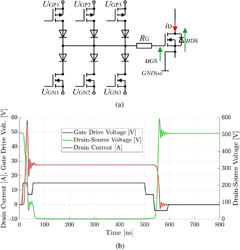
In this category, a predefined voltage profile is applied to the gate of a MOSFET. Waveforms for these methods are generalized in Figure (b), with a schematic in Figure (a).
Figure 5. (a) Generalized voltage-fed AGD and (b) simulated characteristic waveforms for turn-on and turn-off. Middle voltage lasting for
during turn-on and
during turn-off. Resulting rising and falling voltage gradients shown are
and
respectively for
inductive clamped load. Simulation is performed in LTSpice using Wolfspeed C3M0065100K MOSFET.
In [Citation14], a gate drive using four voltage levels was proposed. An ASIC is used to drive the logic of an H-bridge connected to the gate and source. The gate voltage is set to the absolute maximum during turn-on, then reduced to the recommended voltage after . During turn-off, the voltage returns to
after the complementary transistor turns on, resulting in a faster turn-on. The method reduces losses by
, but increases
.
In [Citation15], a similar method is presented that uses an auxiliary circuit triggered by power stage conditions to reduce voltage and current gradients during turn-on and turn-off. The gate voltage is reduced to minimize losses and shorten the turn-on delay time. A comparator is triggered by the parasitic inductance of the source to reduce the output voltage, and after a defined delay time, the output voltage returns to the standard value. This process is reversed during turn-off, reducing overshoot and EMI. Compared to CGD, current overshoot is reduced twofold and voltage overshoot by for the same turn-on losses.
In [Citation16], a described method uses multiple voltage levels only during turnoff. A positive intermediate voltage is used, which can temporarily put the transistor in the saturation region, depending on the set level. The operating principles are similar, with predefined instances of setting the medium voltage level and returning to the allowed negative voltage. However, the method requires additional care due to the effect of threshold voltage reduction with increasing temperature.
The method described in [Citation17] uses voltage-fed AGD to characterize and extract the SiC MOSFET switching parameters. It uses multiple gate drives between multiple voltage rails. The control logic is on the primary side, while the level-shifting is executed through signal isolators. The results are arranged in maps as it will be done in this paper, however, different variables are evaluated, such as overshoot voltage, and no optimization nor other influences is used to determine the optimum mid-level voltage time.
4.1.3. Variable resistance gate driver
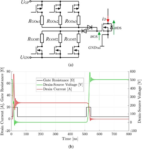
Similar to the aforementioned, all resistive methods aim to reduce voltage and current gradients and accelerate transients in the remaining subintervals of the switching, and as such can be seen in Figure (b), with schematic in Figure (a).
Figure 6. (a) Generalized variable resistance gate driver and (b) simulated response for turn-on and turn-off, and
, with increased resistance lasting
during rise and fall times. Resulting rising and falling voltage gradients shown are
and
respectively for
inductive clamped load. Simulation is performed in LTSpice using Wolfspeed C3M0065100K MOSFET.
A broadly applicable method described in [Citation18] changes the gate resistance in four stages and reduces current overshoot from to
, with lower switching losses by
. In turn-on and turn-off, it utilizes initial and final values of
and
during switching transients. Using the drain-source voltage divider and the shunt in the source, the current and voltage are measured and used to trigger resistance switchover, with triggering reference values also being adjustable with a DA converter.
The method described in [Citation19] uses two resistance levels for turn-on and turn-off and is measuring , using it as feedback to adjust the switching trajectory using comparators. In right conditions, the method reduces
from
to
and
from
to
, while simultaneously increasing losses by approximately
. This method can be improved by dynamically changing the comparator thresholds as favourable operating conditions occur for a narrow operating point range.
The method [Citation8] has current feedback using a shunt connected to the source. The method uses main and two auxiliary resistors, where one of the auxiliary resistors assists during turn-on, and the other during turn-off during current and voltage rise times. The time intervals in which the additional resistors will be turned on are defined with thresholds that, depending on the current, are changed by the DA converter. The method successfully reduces the voltage overshoot from to
with an increase in turn-off losses from
to
.
4.1.4. Capacitor-assisted active gate drivers
Krishna and Hatua [Citation20] describe a method for turning on and off a SiC MOSFET using three p-channel and three n-channel MOSFETs to indirectly control the charge injected into the gate. There are three complementary stages during turn-on and turn-off. The first transistor is used as a current source, the second as a capacitive impulse charge, and the third transistor completes the turn-on. The method prolongs by
and reduces overshoot peak from
to
.
In [Citation21] method for faster turn-off using an auxiliary capacitor to decrease the time spent in Miller's plateau is proposed. The MOSFET is first turned on through a single gate resistor, after which the second one is added in parallel. In turn-off, the gate is discharged with a current spike through a capacitor after which a Miller clamp is turned on. The method reduces turn-on losses by , but may not be efficient beyond the design operating point.
4.1.5. Resonant SiC MOSFET gate drives
Resonant drivers contain inductors connected to the gate which are current-biased and improve the speed of gate charging.
One of the proposed resonant methods evaluates the temperature dependence of MOSFET parameters [Citation22]. The method uses the peak gate current as temperature detection. The resonant gate drive is composed of an H-bridge with an air-core inductor. The circuit pre-charges the coil by connecting it between supply rails. Then low-side transistor is turned off with an inductor discharging through the gate in on-state, another high-side transistor pulls the gate to the positive rail. The inductor is then negatively pre-charged (mirror-symmetrical to turn-on) for turn-off and later clamped to negative rail. The method has been validated only on low DC link voltage.
Method described in [Citation23] uses a p and n-channel pair with a diode-inductor connection between them. One end of the inductor is also connected to the gate of the SiC MOSFET. In turn-on, the p-channel driver turns on, while the n-channel driver delays its turn-off, pre-charging the inductor. After a predetermined delay, the n-channel MOSFET turns off and the inductor discharges to the gate. By natural commutation, the current of the inductor drops to zero. The turn-off clamps the gate and source with an n-channel transistor. The method was tested on a boost converter with output voltages and
. The switching losses were reduced by
, while the current rise time was shortened from
to
. A common disadvantage of resonant gate drive is the inherent lengthening of the dead time, which introduces a delay in the control loop.
4.1.6. Current source gate drivers
Second method introduced in [Citation22] and method [Citation24] use controlled but unadjustable current mirrors during turn-on. A pair of p-channel MOSFETs or PNP BJTs are connected to the positive rail and used as current sources. The disadvantage of the method is the difficulty of achieving symmetrical switching of the SiC MOSFET, as a current sink is also required for this. Thus, only a turn-on is often realized, while the turn-off uses a single pulldown to a negative voltage or 0 V. However, Pilli et al. [Citation24] show improvements in terms of shorter turn-on delay times, which expands the bandwidth of a main control loop. For increased turn-off losses of and increased turn-on losses of
there is a decrease in
in turn-off by
and
in turn-on of
.
Additionally, the variable current source method described in [Citation25] uses inductive components in an H-bridge-like topology with an auxiliary leg to pre-charge and release the gate current while limiting the oscillatory behaviour of the gate loop. The method is able to produce two gate current pulses, which aims to decouple from
control. The method reduced the switching losses, but it increased
. The main application are dead-time sensitive topologies like dual-active bridge, as it reduces turn-on and turn-off delay times.
4.2. Advanced and closed loop IGBT gate drivers
Since the IGBT is a mature semiconductor technology, the most advanced active switching methods are more developed than for SiC MOSFETs. An additional advantage is lower switching speed, which makes it significantly easier for IGBTs to achieve closed-loop control. Below is an overview of methods that have been developed exclusively for IGBTs.
4.2.1. Gate drives for IGBT with closed loop and control
The most advanced methods control the and
in a closed loop, with step-functions as the references of gradients. The [Citation26] method uses mostly analogue control and it assumes that
is zero during voltage rise and fall times. This enables a common control loop for current and voltage gradients with an analogue PI controller. The method was validated on IGBT modules and when compared to a CGD a reduction of turn-on losses by
times and turn-off losses by
times were seen, with
increasing 4 times.
4.2.2. Drivers with real-time trajectory management
Due to parameter variability (temperature, load current, etc.), method [Citation27] uses adaptive real-time switching control on an FPGA, where a parametric lookup table (LUT) for the gate voltage sequence is used. Individual switching stages are detected by a comparator circuit. A DA converter sets the current source reference. Adaptive control uses a signum algorithm optimization.
The [Citation28] method uses voltage drive as in Figure (a), but with 64 possible voltage levels in 60 time slots. This switching sequence is then prepared in the FPGA every second. An external device measures and evaluates the output currents and voltages of the IGBT and determines the next switching sequence with the optimization algorithm adaptable to parameter changes. The method reduces switching losses up to , using voltage overshoot as a constraint variable.
A method similar to the previous, but utilizing 64 current sources is likewise applied to IGBT and uses in-the-loop optimization with a particle-swarm algorithm, however, it requires high performance hardware such as PC to run optimization during converter operation [Citation29].
4.3. Optimization methods for SiC MOSFET switching
The methods which feature variously applied optimization techniques in different scenarios are the current state-of-the-art. The basic method described in [Citation30] uses the four-level active gate drive with continuously adjustable gate voltages. It extracts datasheet parameters to optimize for ,
and switching losses. However, it does not utilize the variability of mid-level time, but rather mid-level voltage only, which limits its controllability range. Also, the method does not vary its parameters regarding load current or DC-link voltage and would greatly benefit from the improved model by using real test values, as neither parasitic elements nor device-to-device variations are accounted for in the datasheet. As the method is not compared to the results of conventional gate drive, it is difficult to evaluate its effectiveness.
Today's most advanced method has been presented in [Citation31]. It uses artificial neural networks (ANN) with variable gate resistances to optimize the active gate drive. A neural network is trained offline with a recorded dataset, and the ANN outputs a mid-level resistance duration depending on external circuit parameters. The method yields lower average
for the same switching losses but requires a large dataset for training and the control in the low current range is very limited.
5. Switching optimization with an AGD
The most prevalent active gate driving methods use either variable voltage or variable resistance. The reason is the similarity to the conventional gate drive, as the logical progression to adding complexity is typically adding one more level of either voltage or gate resistance during turn-on or turn-off. As seen in the previous chapter, gate drivers are commonly voltage sources with external gate resistances for turn-on and turn-off, models of which are well-known and have been studied thoroughly. For the selected gate drive topology, voltage-fed AGD with separate levels for turn-on and turn-off is selected to be further examined. This is because current source drivers typically introduce a delay or have drive strength or bandwidth issues [Citation32], while other topologies require a deeper understanding of their influence on the switching process in all modes of converter operation, including failures. Due to the relatively simple output stage and more straightforward component selection, which do not feature energy storage, it is uncomplicated to envisage voltage-fed AGD usage in power converters both at discrete and IC levels.
Considering the findings in the previous chapters, a gate voltage profile can be optimized for every switching event. This means that the part of the EMI spectrum on which the gate drive has influence is kept constant under every switching condition regardless of load current (), semiconductor temperature, etc. It will later be shown that since
and
are monotonically increasing functions, the optimum switching will be achieved for the shortest possible mid-level time (
). To generalize this problem, it is possible to map out all of the possible switching sequences for a certain active gate drive. If the half-bridge observed is symmetrical, i.e. uses the same transistor for the high and low sides, then also mapping a single direction of current is sufficient to find all of the possible switching states. For the reverse current direction, the diagonally opposite diode and transistor pair commutate, however, the switching events remain the same.
5.1. Methodology of gate drive mapping
As Section 2 has shown, for a given transistor, its is dependent on the half-bridge load current, gate resistance, and the injected gate voltage. Furthermore, gate voltage shaping has yielded favourable results in previous works [Citation28]. For the context of this paper, gate voltage threshold temperature dependency will be ignored, however, this additional parameter can be included in a physical setup. If a “pre-mapping” of a switching device exists, then an optimum voltage sequence can be generated at the gate given the power stage conditions i.e. load current and required
.
To confirm the validity of this concept, a simulation framework that generates maps of the versus load current
and various gate voltage sequences during turn-on and turn-off was implemented. The mapping is achieved through a MATLAB script which executes LTSpice as a simulation tool with an appropriate gate drive voltage sequence. For each load current condition i.e. from 0 to rated and for each voltage level and each voltage-level duration, a piece-wise linear (PWL) file is generated and Spice simulation is started by a command prompt batch file. The simulation performs a single pulse test with a current source as a load. After the Spice simulation converges, the output file is read back to MATLAB where
during both turn-on and turn-off is read as rise time. The turn-on or turn-off switching energy are calculated from the results of the same simulation as (Equation40
(40)
(40) ) and (Equation41
(41)
(41) ):
(40)
(40)
(41)
(41) Since the sampling time of the Spice tool is variable, the points are linearly interpolated to a sample time of
. The
values are taken as average on a time interval from
to
of DC-link voltage. After the calculation, the results are saved to a map and a new simulation is started with the next circuit parameters and a new gate voltage profile PWL file. The resulting map is a discrete function of two variables
with gate resistance
, mid-level gate voltage
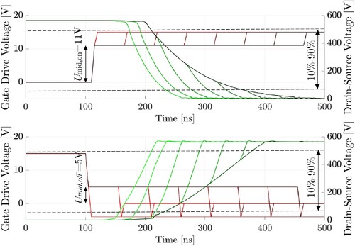
and voltage sequence type as a parameter. In this paper, two sequences were examined, namely “pullback-like” (as in Figure (b)), and “staircase-like” sequences (as in Figure ). In each examined case, the DC-link voltage was set to
. To enhance global convergence, the simulation circuit excludes external parasitic elements, such as commutation loop inductances, because they do not affect
, but rather influence
, justifying their omission. As Figure suggests, the drain-source voltage of a transistor, and therefore half-bridge AC node, is broken in two distinct sections, i.e. section during
with low
, and section after
with high
, for both turn-on and turn-off.
Figure 7. Gate voltage sequences: and
for turn on and turn-off. Displays simulated signal shaping and
duration influence on
for IMZ120R045M1. The mid-level gate drive voltages are
and
. The selected duration
ranges from 0 to
in
increments. Simulation is performed with
, and with load current of
.
5.2. Direct maps
To optimize the switching, both turn-on and turn-off maps need to be examined. Since the plateau voltage varies with current, is temperature-dependent and varies for turn-on and turn-off [Citation6]. Turn-on and turn-off events were mapped with different
voltages in the appropriate range for possible Miller plateau levels (this is transistor-dependent). The reasoning behind
and
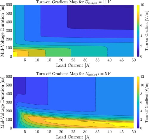
selection will be explained in the upcoming subsection. The resulting maps are shown in Figure . Examining the two different sequences (i.e. “pullback” and “staircase”), the “staircase” sequence was selected because of its straightforward hardware realization, safety (no re-turn off is possible after the current commutation) and a lack of additional timing parameters (peak-gate voltage duration before “pullback”).
Figure 8. A contour plot of direct maps for turn-on and turn off of Infineon IMZ120R045M1 SiC MOSFET in half-bridge. DC-link voltage used is
. External
is used to provide a balance of controllability and achievable time resolution. Gate time constant is
. A high-sensitivity area can be observed for a range of
to
. Voltages of
and
are selected from a set of maps to optimize between controllability and losses. Similar results were obtained for Cree C3M0065100K SiC MOSFET.
5.3. Map inversions and optimum switching time
Optimum switching requires knowing the exact mid-voltage () pulse duration (
) and its value given the current condition and required
. The goal is to minimize switching energy for turn-on and turn-off while keeping
as constant as possible. To obtain the inverted map, i.e.
the direct maps need to be restricted to their monotonic intervals. This is because an inverse of a function exists if and only if each input point corresponds to a single unique output point (bijective function).
For both turn-on and turn-off, the area for which the function is defined (i.e. domain) is bounded by two curves. This is also the area where can be controlled, and has to be taken into consideration. This is the controllability area and is the domain of the inverted function
and can be bounded by four lines for turn-off, and two for turn-on.
5.3.1. Turn-on area of controllability
The area in which turn-on gradient can be controlled is bounded by two curves. The upper bound is defined by the expression (Equation42(42)
(42) ), and corresponds to
when
is too short to influence the switching. For this case, mid-level voltage is shorter than turn-on delay, i.e.
holds.
(42)
(42) The lower bound is defined by the relation (Equation43
(43)
(43) ). In this case
lasts longer than Miller plateau time, and
holds.
(43)
(43)
5.3.2. Turn-off area of controllability
For turn-off, non-linear curves are approximated as piecewise linear lines, as in (Equation23(23)
(23) ). The upper bound of the area of controllability is defined by (Equation44
(44)
(44) ) and corresponds to the
curve when
is too short to influence the switching. Here
holds.
(44)
(44) Conversely, the lower bound of the area of controllability is defined by the curve (Equation45
(45)
(45) ). In this case,
lasts longer than Miller plateau time, and AGD can no longer influence
in switching. Here
holds.
(45)
(45) For both cases, currents
and
can be calculated as:
(46)
(46)
(47)
(47)
Inverted maps in Figures and were obtained using a search algorithm. Before, upper and lower boundaries were set to limit the search to a controllable area. In practice, a 2D cross-section of the direct map was found first and the longest monotonic sequence was extracted from it to obtain the search boundaries. Then, an optimum point for which is satisfied is found with sequential quadratic programming method, which yields a single inverted map point. The algorithm is repeated for all
and
vector points.
5.4. Gate resistor and mid-voltage selection
From Equations (Equation42(42)
(42) )–(Equation45
(45)
(45) ) it can be seen that
greatly influences the area of controllability. In general, gate resistance for AGD must be selected low enough so that it does not limit the upper bounds of controllability and can achieve fast enough
for shortest
times, Also, gate resistance needs to be high enough to allow for achievable
time resolutions to influence switching in a physical setup using FPGA (for example in around nanosecond range), though for SiC devices, typical
is in the range of
up to
for large modules, which yields controllable gate time constants.
Figure 9. A contour plot of inverted maps for turn-on with
and
, and for
. The controllability area is maximized for
. A tradeoff exists between the area of controllability and total losses. The highest difference is seen for large drain currents.
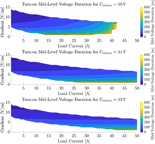
Figure 10. A contour plot of inverted maps for turn-off
and
and for
. The area of controllability is maximized for
, however, lower losses are achieved for
. Controllability is severely limited for
.
Additionally, to improve the overall EMI performance of AGD further, the for AGD needs to be empirically in the range of
to
of the CGD
needed for the required
to minimize the slope of individual
pieces (Figure ).
To minimize losses, has to be selected so that it is as low as possible for turn-off and as high as possible for turn-on, while
is still controllable for the required current range.
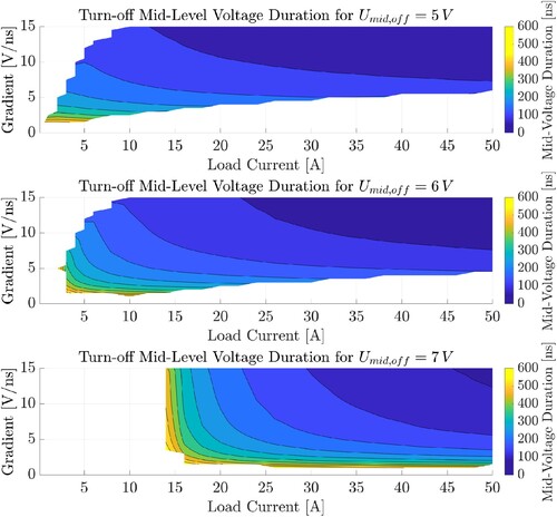
5.5. Switching losses
For CGD, losses can be estimated according to [Citation33]: (48)
(48)
(49)
(49) Where
are losses due to reverse recovery. Relationship between
and
is non-linear, however since it is monotonic for observed mid-level times, the optimum switching strategy is to select the lowest possible
which yields selected
, for example
. This way losses are minimized in every switching cycle. As switching energy is also calculated alongside
values, it is arranged for turn-on and turn-off in a map as depicted in Figure as well. The figure also highlights the optimum switching trajectory for constant
gradient.
Figure 11. Switching loss map of IMZ120R045M1 with optimum switching path for currents up to
highlighted. For turn-off, AGD affects switching above
for any combination of
and
.
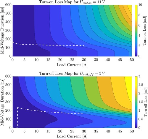
6. Experimental verification
To verify the findings from the previous chapter, a special test setup has to be designed. Since no commercial gate driver allows for slope shaping by dynamically changing and
in both turn-on and turn-off events, Infineon 1ED3890 was selected as an appropriate IC for turn-off gradient control only. The device settings are reconfigurable through I2C, where turn-off
can be reconfigured in
steps analogous to waveforms in Figure . In addition, the test fixture was developed in a half-bridge configuration with the possibility of interchanging the gate drive PCBs for further research. The current measurement was performed with PEM CWT1 Rogowski coil, and the voltage measurement was made using two Tektronix THDP0200 differential probes with short voltage clips to reduce couplings as is depicted in Figure .
Figure 12. Test setup for experimental verification of direct maps, consisting of HVDC source, inductor and PC with UART communication to main MCU for test parametrization.
The setup is automated and the pulse sequence is controlled through a microcontroller (MCU) stacked on top of the gate drive board which is depicted alongside the half-bridge test fixture in Figure . The MCU controls the duration of a single pulse, i.e. the PWM pin of the low-side SiC device, and reconfigures pulse duration (i.e. load current), mid-voltage duration and mid-voltage level
with a 3-second pause in between. The oscilloscope is set to store every shot captured in normal mode. The current is controlled with pulse duration in
to
range, while
is controlled in
to
range and
from
to
in
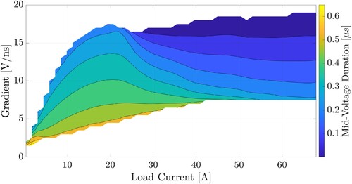
steps. In total, 1056 shots for transistor current, drain-source voltage and gate-source voltage were captured, their value later extracted and fitted to a map depicted in Figure for
.
Figure 13. Test hardware PCB stack depicting the (a) gate drive (GD) and (b) half-bridge with bulk capacitance and
Cera-Link capacitor. Additional high and low-side transistor footprint slots are added for potential usage in parallel testing.
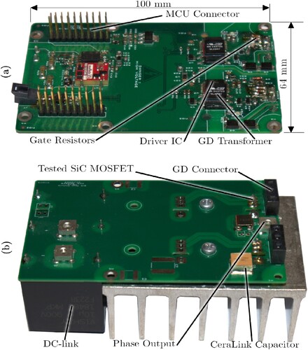
Figure 14. Scatter plot of measured points in an experimental verification of direct maps on a half-bridge setup for IMZ120R045M1. The DC-link voltage used is with gate resistance of AGD
, and with
of
.
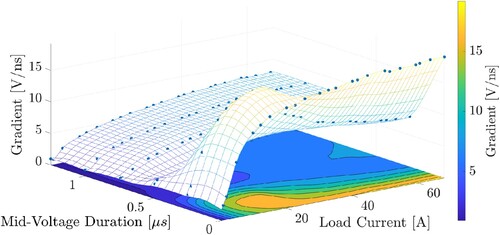
Although the direct comparison of maps is not possible due to differences between setup and simulation, i.e. differences in gate resistance, the existence of parasitics in the commutation loop and production tolerances, maps can be qualitatively compared. The performance measurements show that during turn-off events can be controlled by applying different durations of mid-voltage levels similarly as was predicted by the simulations. Moreover, the measurements show that the shape of the map from Figure qualitatively follows Figure , therefore justifying the usage of the proposed method.
Furthermore, by interpolating measured points to a finer grid, an inverted map with visible controllability area can be obtained as in Figure . An inverted map was obtained using the method described in the previous chapter. Having the current dependant inverted map datasets pre-loaded in an MCU or FPGA enables a cycle-by-cycle control on an improved hardware setup that is currently under construction. Although the proposed method could be applied to many topologies which use a half-bridge as a building block, the automotive three-phase inverters are seen as the best candidate due to their beneficial influence on common mode and high demand in the future.
Figure 15. A contour plot of an experimental inverted map for DC-link voltage and
with
. Areas of controllability have been following a similar domain shape as with inverted simulated maps.
7. Simulated validation of optimized switching strategy
To compare the optimum switching strategy to the conventional gate drive, a simulated application of the three-phase inverter was employed. The three-phase inverter model consisted of six IMZ120R045M1 SiC MOSFETs. Six PWL files containing optimized injected gate voltages as well as load current signals were generated using MATLAB script. This way cycle-by-cycle control is employed and any operating point for the inverter could be tested.
In general, can be kept constant to limit the insulation strain and minimize peak EMI noise. For standard industrial drives, a typical limit of
to
is employed [Citation34]. Mid-level time duration
for input
and required
is extracted from the inverted map and fitted to a polynomial. Moreover, for the uncontrollable parts of the switching cycle, i.e. when
, duration
is set.
Parasitics were omitted from the main simulation circuit to take the worst possible case of into the account, since additional parasitic slow down the switching further. To evaluate the active gate drive performance, the simulation uses worst-case modulation index for CM noise (
or
). This is because all of the three phases of the inverter then switch simultaneously and therefore generate a square wave-like CM voltage of triple the fundamental frequency instead of a stepped sine wave, like for high modulation indexes. The simulated time-domain common-mode signal was then fed to a virtual EMI receiver [Citation35] for
RBW, sweeping from
to
. The resulting spectral response is depicted in Figure (a).
Figure 16. (a) Spectral response of peak CM noise of a three-phase inverter for RBW in
steps and from
to
, and (b)
in turn-off for every switching cycle for a sinusoidal current. Turn-on
is symmetric along zero-crossing. Switching frequency used is
with a fundamental output frequency of
, while load current sine wave peak is
. AGD exploits the unused area close to
as much as possible.
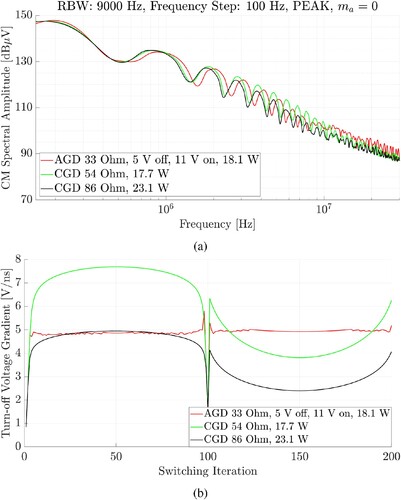
The comparison between the optimized AGD, equivalent losses CGD and equivalent maximum CGD has been shown in Table . While Peak CM emissions remain in the same range, Figure shows that the time-dependent
curve using AGD is fixed to
. CGD reaches set
level in just one operating point, significantly increasing the losses.
For practical application, inverted maps can be pre-loaded into a DSP, so that close to optimal time can be found cycle-by-cycle. Small corrections to
for temperature and DC-link voltage dependency with predictive methods could be employed to compensate for modelling inaccuracies.
Table 3. Optimized AGD and CGD inverter parameters and comparison.
8. Conclusion
SiC MOSFETs can now be used as easily as Si MOSFETs or IGBTs, with improved performance and potential for widespread use. The higher cost of SiC-based converters and potential EMI issues are the main obstacles to their adoption. Broader use is expected to bring costs down, while EMI issues could be reduced by passive filters or with appropriate conventional gate driving.
In this paper, an overview of various active and advanced gate driving techniques were studied with several design practices for conventional SiC-based converters. Existing advanced solutions adjust the gate voltage or resistance to dynamically change the and/or
. Typically, the advanced methods shorten the remaining transient phenomena after the transitions.
This paper gives the simplified switching model, which can be applied to both CGD and AGD. More importantly, an advanced and optimized active gate driving strategy with an explanation of underlying phenomena was introduced.
Within this, a strategy for cycle-by-cycle optimization of SiC MOSFETs switching is proposed to enable trade-off between switching losses and by keeping
as close to constant as possible. The method yielded
lower total losses for the same maximum
, with peak EMI within the same range. Employing the proposed method has shown that there is still room for improvement in active gate driving strategies.
taut_a_2362525_sm5028.png
Download PNG Image (779.4 KB)
taut_a_2362525_sm5033.png
Download PNG Image (271.8 KB)
taut_a_2362525_sm5037.png
Download PNG Image (890.1 KB)
taut_a_2362525_sm5039.png
Download PNG Image (756 KB)
taut_a_2362525_sm5030.png
Download PNG Image (408.7 KB)
taut_a_2362525_sm5040.png
Download PNG Image (562.5 KB)
taut_a_2362525_sm5031.png
Download PNG Image (293.5 KB)
taut_a_2362525_sm5032.png
Download PNG Image (341.1 KB)
taut_a_2362525_sm5029.png
Download PNG Image (682 KB)
taut_a_2362525_sm5035.png
Download PNG Image (1.3 MB)
taut_a_2362525_sm5026.png
Download PNG Image (309.6 KB)
taut_a_2362525_sm5038.png
Download PNG Image (422.2 KB)
taut_a_2362525_sm5034.png
Download PNG Image (468.8 KB)
taut_a_2362525_sm5025.png
Download PNG Image (73.8 KB)
taut_a_2362525_sm5043.png
Download PNG Image (389.9 KB)
taut_a_2362525_sm5036.png
Download PNG Image (74.7 KB)
taut_a_2362525_sm5027.png
Download PNG Image (5.2 MB)
taut_a_2362525_sm5024.jpg
Download JPEG Image (981.2 KB)
taut_a_2362525_sm5042.png
Download PNG Image (254.5 KB)
taut_a_2362525_sm5041.png
Download PNG Image (669.8 KB)
Disclosure statement
No potential conflict of interest was reported by the author(s).
References
- Oswald N, Anthony P, McNeill N, et al. An experimental investigation of the tradeoff between switching losses and EMI generation with hard-switched All-Si, Si-SiC, and All-SiC device combinations. IEEE Trans Power Electron. 2014;29(5):2393–2407. doi: 10.1109/TPEL.2013.2278919
- Haider M, Fuchs S, Zulauf G, et al. Analytical loss model for three-phase 1200 V SiC MOSFET inverter drive system utilizing Miller capacitor-based dv/dt-limitation. IEEE Open J Power Electron. 2022;3:93–104. doi: 10.1109/OJPEL.2022.3143995
- Ivaniš T, Kovačić M. An overview of advanced gate driver concepts for SiC semiconductors. In: 2023 International Conference on Electrical Drives and Power Electronics (EDPE). Slovakia: The High Tatras; 2023. p. 1–9.
- Hegarty T. Texas instruments, The engineer's guide To EMI In DC-DC converters (Part 3): understanding power stage parasitics. Application note; March 2018.
- Kovacevic-Badstuebner I, Stark R, Grossner U, et al. Parasitic extraction procedures for SiC power modules. In: CIPS 2018; 10th International Conference on Integrated Power Electronics Systems. Stuttgart, Germany; 2018. p. 1–6.
- Liu S, Song S, Xie N, et al. Miller Plateau corrected with displacement currents and its use in analyzing the switching process and switching loss. Electronics. 2021;10:2013. doi: 10.3390/electronics10162013
- Wu Y, Li H, Li C, et al. Analytical modeling of SiC MOSFET during switching transient. In: 2018 IEEE International Symposium on Electromagnetic Compatibility and 2018 IEEE Asia-Pacific Symposium on Electromagnetic Compatibility (EMC/APEMC). Singapore; 2018. p. 1187–1192.
- Acharya S, She X, Tao F, et al. Active gate driver for SiC-MOSFET-based PV inverter with enhanced operating range. IEEE Trans Ind Appl. 2019;55(2):1677–1689. doi: 10.1109/TIA.2018.2878764
- Kasper M, Burkart RM, Deboy G, et al. ZVS of power MOSFETs revisited. IEEE Trans Power Electron. 2016;31(12):8063–8067.
- Nayak P, Hatua K. Modeling of switching behavior of 1200 V SiC MOSFET in presence of layout parasitic inductance. In: 2016 IEEE International Conference on Power Electronics, Drives and Energy Systems (PEDES). Trivandrum; 2016. p. 1–6.
- Hegarty T. Texas instruments, The engineer's guide to EMI in DC-DC converters (Part 2): noise propagation and filtering. Application note; January 2018.
- Oswald N, Stark BH, Holliday D, et al. Analysis of shaped pulse transitions in power electronic switching waveforms for reduced EMI generation. IEEE Trans Ind Appl. 2011;47(5):2154–2165. doi: 10.1109/TIA.2011.2161971
- Peftitsis D, Rabkowski J. Gate and base drivers for silicon carbide power transistors: an overview. IEEE Trans Power Electron. 2016;31(10):7194–7213.
- Zhang Z, Dix J, Wang FF, et al. Intelligent gate drive for fast switching and crosstalk suppression of SiC devices. IEEE Trans Power Electron. 2017;32(12):9319–9332. doi: 10.1109/TPEL.2017.2655496
- Yang Y, Wen Y, Gao Y. A novel active gate driver for improving switching performance of high-power SiC MOSFET modules. IEEE Trans Power Electron. 2019;34(8):7775–7787. doi: 10.1109/TPEL.63
- Zhao S, Dearien A, Wu Y, et al. Adaptive multi-level active gate drivers for SiC power devices. IEEE Trans Power Electron. 2020;35(2):1882–1898. doi: 10.1109/TPEL.63
- Philipps DA, Xue P, Ubostad TN, et al. Low inductive characterization of fast-switching SiC MOSFETs and active gate driver units. IEEE Trans Ind Appl. 2023;59(5):6384–6398. doi: 10.1109/TIA.2023.3282930
- Nayak P, Hatua K. Active gate driving technique for a 1200 V SiC MOSFET to minimize detrimental effects of parasitic inductance in the converter layout. IEEE Trans Ind Appl. 2018;54(2):1622–1633. doi: 10.1109/TIA.2017.2780175
- Camacho AP, Sala V, Ghorbani H, et al. A novel active gate driver for improving SiC MOSFET switching trajectory. IEEE Trans Ind Electron. 2017;64(11):9032–9042. doi: 10.1109/TIE.2017.2719603
- Krishna MV, Hatua K. An easily implementable gate charge controlled active gate driver for SiC MOSFET. In: IECON 2018 – 44th Annual Conference of the IEEE Industrial Electronics Society. Washington (DC); 2018. p. 999–1004.
- Yamaguchi K, Katsura K, Yamada T, et al. Comprehensive study on gate driver for SiC-MOSFETs with gate boost. IEEJ J Ind Appl. 2018;7(3):218–228. Online ISSN 2187-1108, Print ISSN 2187–1094.
- Niu H, Lorenz RD. The effect of gate drive topology on online silicon carbide MOSFET junction temperature sensing. In: 2015 IEEE Energy Conversion Congress and Exposition (ECCE). Montreal (QC); 2015. p. 7015–7022.
- Anthony P, McNeill N, Holliday D. High-speed resonant gate driver with controlled peak gate voltage for silicon carbide MOSFETs. IEEE Trans Ind Appl. 2014;50(1):573–583. doi: 10.1109/TIA.28
- Pilli NK, Chauhan AK, Singh SK, et al. An inductor-less, discontinuous current source gate driver for SiC devices. IEEE Access. 2019;7:34227–34237. doi: 10.1109/Access.6287639
- Rødal GL, Peftitsis D. An adaptive current-source gate driver for high-voltage SiC mosfets. IEEE Trans Power Electron. 2023;38(2):1732–1746. doi: 10.1109/TPEL.2022.3208827
- Lobsiger Y, Kolar JW. Closed-loop di/dt and dv/dt IGBT gate driver. IEEE Trans Power Electron. 2014;30(6):3402–3417. doi: 10.1109/TPEL.2014.2332811
- Dang L, Kuhn H, Mertens A. Digital adaptive driving strategies for high-voltage IGBTs. In: 2011 IEEE Energy Conversion Congress and Exposition. Phoenix (AZ); 2011. p. 2993–299.
- Cheng YS, Mannen T, Wada K, et al. Optimization platform to find a switching pattern of digital active gate drive for reducing both switching loss and surge voltage. IEEE Trans Ind Appl. 2019;55(5):5023–5031. doi: 10.1109/TIA.28
- Cheng YS, Yamaguchi D, Mannen T, et al. High-speed searching of optimum switching pattern for digital active gate drive to adapt to various load conditions. IEEE Trans Ind Electron. 2022;69(5):5185–5194. doi: 10.1109/TIE.2021.3084169
- Du X, Wei Y, Stratta A, et al. A four-level active gate driver with continuously adjustable intermediate gate voltages. In: 2022 IEEE Applied Power Electronics Conference and Exposition (APEC). Houston (TX), USA; 2022. p. 1379–1386.
- Wiesemann J, Dumtzlaff J, Mertens A. Control of an active gate driver for an electric vehicle traction inverter using artificial neural networks. In: 2022 24th European Conference on Power Electronics and Applications (EPE'22 ECCE Europe). Hanover, Germany; 2022. p. 1–10.
- Patmanidis K, Kist T, Glavanovics M, et al. Configurable gate driver for a stress test bench of newly developed discrete silicon power devices. Microelectron Reliab. 2021;124:Article ID 114283. doi: 10.1016/j.microrel.2021.114283
- Christen D, Biela J. Analytical switching loss modeling based on datasheet parameters for mosfets in a half-bridge. IEEE Trans Power Electron. 2019;34(4):3700–3710. doi: 10.1109/TPEL.2018.2851068
- Velander E, Bohlin G, Sandberg Å, et al. An ultralow loss inductorless dv/dt filter concept for medium-power voltage source motor drive converters with SiC devices. IEEE Trans Power Electron. 2018;33(7):6072–6081. doi: 10.1109/TPEL.63
- Bendicks A, Dörlemann T, Krause C, et al. MATLAB/Octave function to evaluate time-domain signals according to the measurement bandwidth and average/peak detector of EMI test receivers. In: Proceedings Conference on Electromagnetic Compatibility. Cologne, Germany; 12–14 July 2022.