
 ?Mathematical formulae have been encoded as MathML and are displayed in this HTML version using MathJax in order to improve their display. Uncheck the box to turn MathJax off. This feature requires Javascript. Click on a formula to zoom.
ABSTRACT
An accurate method to model the optical behaviour of liquid crystal (LC) devices, particularly suited to devices where diffractive effects are present is described here. An accurate electromagnetic modelling programme that takes into account the full non-uniformity and anisotropy of the LC has been developed. This is combined with an existing in-house LC finite element modelling programme based on the Landau – De Gennes theory, that uses the order tensor representation of the LC orientation and allows an accurate descriptions of structures containing LC defects and small features. The electromagnetic model is based on the total field/scattered field (TF-SF) approach to electromagnetic scattering problems and is implemented using finite differences in the frequency domain (FDFD) in a form that can accommodate perfectly matched layers (PMLs) and periodic boundary conditions. The resultant matrix problem is solved efficiently using an especially adapted form of a sweeping preconditioner and the generalised minimum residual method (GMRes). This method has been implemented in 2D and is demonstrated here with the design and analysis of a reconfigurable blazed phase grating that utilises an LC defect to produce an abrupt fly-back, with the capability of short periods and high diffraction efficiency.
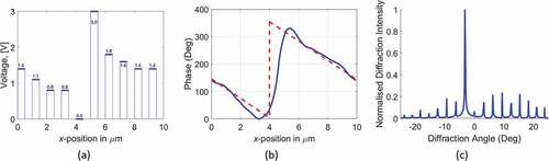
GRAPHICAL ABSTRACT
1. Introduction
In comparison with other commonly used optical materials, liquid crystals (LC) have a large birefringence that can be controlled with relatively low electric fields, making them very attractive for many photonic, microwave and terahertz applications. In photonics, apart from traditional displays, they are ubiquitous in diffractive devices, programmable holograms and spatial light modulators, with applications in communications and many other fields [Citation1–7] and more recently, LC geometric phase lenses for beam steering, microscopy, laser tweezing and LiDAR [Citation8–11]. Diffractive LC devices are also the basis for new display systems such as head-up, holographic, diffractive and 3D displays [Citation12], and in general, applications where phase modulation is necessary, something that is not possible with emissive systems. Another range of applications is in shaping and controlling electromagnetic wave propagation in photonics, microwave and terahertz waveguiding devices [Citation13–17].
In many of these applications, changes in the material characteristics (LC orientation, presence of defects) and dimensions of the device features and size and spacing of electrodes, occur at length scales comparable to the wavelength used and accurate modelling becomes essential to design and optimise these devices. This includes not only the balance between biasing electric fields and elastic interactions which will determine the LC orientation and then, the permittivity distribution, but also the accurate modelling of electromagnetic wave propagation through this fully anisotropic and non-uniform material.
We describe here a finite difference in the frequency domain (FDFD) method to model electromagnetic wave propagation, combined with a finite element LC model that yields the permittivity distribution for any state of switching of the LC material. A finite element programme based on the Landau-De Gennes theory [Citation18–20] is used to find the distribution of the LC orientation over the LC cell, from which the high frequency or optical tensor permittivity distribution is calculated. This is then imported into the FDFD electromagnetic solver.
The numerical solution of electromagnetic problems of this kind is normally not simple. Fine discretisation of the problem domain is needed and the problem often presents ill-conditioning, which is usually exacerbated by the use of absorbing conditions that are necessary in many problems of interest. All these circumstances combined will cause low convergence rates, long computation times and large memory requirements. To try to overcome these problems, we use here a procedure that combines an adapted form of a sweeping preconditioner [Citation21], within the total field – scattered field (TF-SF) approach to electromagnetic scattering problems [Citation22–26].
The method has been implemented in two dimensions and is demonstrated here with the design and analysis of a reconfigurable blazed phase grating that uses LC defects to introduce an abrupt fly-back and reduced grating period.
Liquid crystal diffraction gratings and spatial light modulators (SLMs) in general, are common component in numerous optical systems. See for example [Citation27,Citation28]. LC-blazed gratings and SLMs are for many applications realised using arrays of LC cells in transmission or commercial liquid crystal on silicon (LCOS) panels for reflective devices, that consist of square pixels with a small inter-pixel gap. The characteristics of the device are determined by the voltages applied to the electrodes in each pixel. In this way, a blazed grating can be realised arranging the voltages in a stepped manner to achieve the desired-phase response [Citation3,Citation29–32], aiming at a piecewise constant phase distribution on the output plane. However, a number of pixels are required for each period of the grating, leading to small deflection angles. In these conditions, defects are unwanted and the inter-pixel crosstalk, although helping to smooth out the phase in the ramped part of the blazed grating, prevents a sharp fly-back. These effects are increased when the pixel size is reduced, which is necessary to achieve larger deflection angles. Here we study how a LC defect can be utilised to introduce a sharp change in LC orientation with the accompanying change in the phase response in the output plane. A preliminary generic design is presented and routes to optimisation are indicated.
2. Theory
2.1. Liquid crystal modelling
The LC modelling used here is based on the Landau – de Gennes theory and describes the local LC orientation and order by the order tensor Q, from where the director and the scalar order parameters can be extracted [Citation18,Citation19,Citation33,Citation34]. The order tensor, or Q-tensor, is symmetric and traceless and can be specified by five scalar values. This formulation, allowing the LC order to vary, is particularly adequate to study LC defects and other situations where the order varies substantially.
A variational approach, implemented with the finite element method in 3D, is used to find the dynamic evolution of the Q tensor distribution that yields stationary values to the Gibbs free energy functional:
where fB is the Landau-de-Gennes bulk thermotropic energy that can be written as a power expansion in the scalar invariants of the Q-tensor about the nematic-isotropic transition and truncated to terms of order four:
where A, B and C are material-dependent parameters.
The elastic distortion energy density fD can be written as an expansion in the gradients of the Q-tensor as:
where are elastic coefficients that can be expressed in terms of the material’s Frank elastic constants and
is the Levi-Civita tensor.
The electric energy density fE, associated to the applied electric fields is given in general by:
where φ is the electric potential
The surface term in (1) corresponds to the anchoring energy that represents the attachment between the LC and the bounding surfaces. This can be described by [Citation19,Citation34,Citation35]:
The principal axes of anchoring are the easy direction and two mutually orthogonal unit vectors such that
. The constants W1 and W2 define the azimuthal and polar surface anchoring strength and a determines the resultant easy surface order.
The modelling of the LC hydrodynamics is done following the approach by Sonnet et al. [Citation36,Citation37], which is numerically equivalent to the Qian and Sheng formulation [Citation38], a generalisation of the Eriksen and Leslie theory for the variable order case. With this, and not considering translational flow, the Q-tensor evolution is characterised by:
where μ1 is proportional to the rotational viscosity and f is the total energy density.
Once the Q-tensor distribution is found, the permittivity distribution is then calculated as where
is the LC director,
is the relative permittivity calculated in the direction perpendicular to the long axis of the LC molecules and
is the dielectric anisotropy.
The solution of the coupled equations that describe the LC physics and the electrostatic potential is implemented using the finite elements method [Citation18–20], to find the dynamic evolution of the LC orientation and order distribution. The problem domain is discretized with a mesh of first-order elements. Neglecting translational flow in the LC, the variables on the nodes of the mesh are the five parameters that describe the Q-tensor plus the electric potential. The solution process consists of a time stepping procedure that calculates iteratively the electric potential and the Q-tensor. At each time step, the potential distribution is found first from the current value of the Q-tensor, and then the Q-tensor is calculated in an iterative nonlinear Crank-Nicolson scheme using Newton-Raphson iterations to deal with the nonlinearity. These calculations are repeated within the same time step until consistency between electric potential and Q-tensor distributions is achieved before progressing in the time stepping procedure.
To accelerate the solution process, variable time stepping is implemented using an estimate of the time derivative error to calculate an appropriate step size. Adaptive mesh refinement has also been implemented to even-up the error distribution and increase the efficiency of the calculations [Citation34].
2.2. Electromagnetic modelling
The propagation of electromagnetic waves through the LC cell is modelled using finite differences in the frequency domain (FDFD) [Citation25,Citation26,Citation39,Citation40]. The calculation method starts by formulating Maxwell’s curl equations in the form [Citation41,Citation42]:
where is the scaled magnetic field and we assume
is scalar and uniform. Taking the curl of the first equation and substituting the second in the right-hand side leads to the Helmholtz equation for the electric field:
Writing this equation in matrix form and assuming uniformity along y for the 2D case gives:
where .
The domain is discretised using a regular rectangular grid and assuming that the general direction of propagation is z, the nodes are numbered following a frontal arrangement based on layers perpendicular to the z-axis. This is an arbitrary choice, a simple addressing strategy and doesn’t restrict the solutions but is convenient if the propagation is predominantly along the z-direction. The discretised form of the equations for the three components of the electric field from (8) are then assembled, forming a vector of unknowns of the form: for each of the nodes of the grid (denoted by the number in the superscript). This arrangement is more convenient than grouping by field component because it yields a more compact sparsity pattern of the resultant matrix. Similarly, a unified vector of the source terms is defined as:
.
EquationEquation (9)(9)
(9) becomes now a matrix equation of the form: A f = g.
2.2.1. Mesh truncation
The problem domain and the corresponding mesh need to be terminated with proper boundary conditions. Electric or magnetic walls, where Dirichlet or Neumann boundary conditions apply, as well as periodic boundary conditions, present no implementation problems and bring no undesired consequences to the solution of the resultant matrix problem. If the domain is naturally unbounded, the mesh is usually terminated using an absorbing boundary condition that prevents outgoing waves to be artificially reflected back into the truncated domain. For this purpose, we use the stretched-coordinate formulation of perfectly matched layers (SC-PML) [Citation43–45]. Although the Uniaxial PML formulation [Citation46] is easier to implement, it has been shown [Citation47] that the stretched-coordinate formulation leads to a global matrix with a lower condition number, which in turn leads to a more efficient matrix solution. To apply the SC-PML, the analytic extension is assumed, where it is customary to choose the frequency-dependent form:
. Setting the coefficient
to zero in the region of interest and with a positive non-zero value in the PML region, the solution of the equations will be an unaltered wave in the region of interest and a wave with exponentially decaying amplitude in the PML. To find the solution, a transformation of coordinates is needed to bring the problem back to the real coordinates: defining
, and similarly
, this is equivalent to transforming the differential operators by:
.
Applying this transformation to EquationEquation (8)(8)
(8) leads to a discretised set of equations for the values of the field components at the nodes of the grid given by the matrix problem: A f = g.
The matrix A has a symmetric sparsity pattern and is symmetric Hermitian if the material is isotropic (not the case of LCs) or if it is anisotropic but lossless. The Hermitian property is also lost if PMLs are used.
The TF-SF approach is a convenient method that was initially developed for the FDTD solution of scattering problems [Citation22–26] and consists of defining equivalent sources on an artificial surface surrounding the scatterer in order to replace the external excitation fields.
Explicit use of the vector g in the right-hand side of the matrix equation is avoided using the procedure presented by Rumpf [Citation25,Citation26], especially adapted to FDFD calculations.
This approach is carried out working with the fully assembled matrix and defining a masking matrix R—a diagonal matrix with 1 and 0 elements in the diagonal – to identify the vector components in the scattered field (SF) and the total field (TF) regions. In this form, the source field values that correspond to the scattered field or to the total field regions can be identified easily as: and
respectively, where
is the excitation field. These expressions can then be used to add or subtract the source terms in the equations corresponding to TF and SF regions, resulting in the right-hand side vector: g [Citation26]:
avoiding the explicit calculation of equivalent sources. The use of the TF-SF approach is particularly useful to make the PML more effective by removing the applied source field incident on PML boundaries and also for the subsequent post-processing of the results.
2.2.2. Solution of the matrix problem
The most time-consuming part of the solution process is the solution of the resultant matrix problem and in consequence the efficiency of the method chosen for this task is important.
For a problem limited entirely by electric or magnetic walls, or by a periodic boundary condition and in the absence of losses, the resultant matrix is Hermitian and there are several adequate methods to solve the matrix problem. However, the presence of losses or the introduction of PMLs will destroy the symmetry and increase the condition number of the matrix. In those cases, a method like GMRes is convenient but the matrix needs to be preconditioned in order to be solved efficiently. In this work, we choose the sweeping preconditioner proposed by Engquist and Ying [Citation21] specially developed to solve matrix problems originated by the numerical solution of the Helmholtz equation. The procedure consists on finding an approximate block LDLT factorisation of the original matrix A and use this as a preconditioner. However, this is done in a block Gauss elimination process that requires the inverse of the diagonal blocks. The basic idea of the method consists of using a frontal ordering approach to the generation of the matrix A, where each of the blocks correspond to layers in the problem domain. With this, the solution for the Schur’s complement in the block Gauss elimination can be seen as the approximate solution of the problem corresponding to just a number of layers which are bounded by absorbing boundary conditions. Sweeping through the domain a number of layers at the time in this manner, will give an approximation of the desired blocks and allow to construct the preconditioning matrix. Although valid for full 3D problems, this preconditioning procedure has been implemented here for 2D problems in conjunction with the TF-SF approach to scattering problems and is demonstrated next with the analysis of a LC diffraction grating.
3. Example of application: a liquid crystal reconfigurable blazed phase grating
The methods described above are used here to demonstrate a reconfigurable LC blazed phase grating that uses the generation of defects to obtain a sharp fly-back.
Traditionally, LC defects were seen as unwanted features that deteriorate the device performance. However, in many devices their presence and evolution are essential to their operation, as for example in the case of bistable displays [Citation48–53].
We present here a basic design for a reconfigurable LC blazed phase grating where a defect is created and used to introduce an abrupt fly-back. This can reduce considerably the grating period and in consequence, increase the possible deflection angles.
3.1. Transmission case
The first case studied here consists of a cell 10 μm wide and with a cell gap (height) of 3.3 μm. Two small electrodes 0.5 μm wide and separated by 0.5 μm are placed in the centre of one surface while the other is covered completely by a ground electrode. The LC material parameters are chosen for this example as those of 5CB, with the values: K11 = 6.4 pN, K22 = 3 pN, K33 = 10 pN, ,
, no = 1.544 and ne = 1.736 [Citation33,Citation54]. While in conventional LC gratings, the alignment is perpendicular to the grating in order to avoid the disclination lines, in this case it is chosen along the same direction of the grating. Periodic boundary conditions are used at the sides of the cell and a pretilt angle of 5° is applied to the top and bottom surfaces.
When the voltage is applied, pincement occurs in the vicinity of the inter-electrode gap and two disclination lines are created [Citation55]. The −1/2 defect line then moves towards the centre of the cell reaching a stationary position in approximately 20 ms while the +1/2 defect remains close to the corner of the driving electrode.
Depending on the applied voltage, the position of the −1/2 defect and the corresponding field distribution over the output plane vary. The results shown in correspond to 5 V applied to one of the bottom electrodes while the other is connected to ground. The top electrode is also fixed to ground. For clarity of illustration, the calculated directors have been here interpolated on a coarse regular grid. Different voltages were tried and it was found that 5 V produced the results that best approximate an ideal blazed grating shape for the phase distribution over the top surface. This also corresponds to the case were the −1/2 defect migrates to the position closer to the middle of the cell gap.
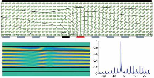
Figure 1. (Colour online) (a) Director distribution and electric potential contour lines when 5 V are applied to one of the bottom electrodes. the circle shows the stationary position of the −1/2 defect, the +1/2 defect remains stationary just above the bottom surface. (b) Field distribution: magnitude of Ex component when a plane wave is normally incident on the bottom surface of the LC layer. Dimensions are in microns; x-z cross-section is shown.
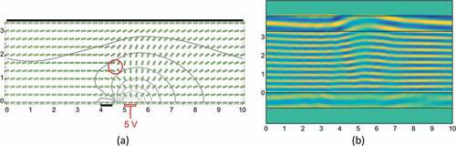
From the director distribution results, the permittivity tensor can be calculated and interpolated onto a regular grid suitable for the FDFD calculation of the electromagnetic response. For this purpose too, the structure is extended at the top and bottom adding a narrow air gap and a perfectly matched layer, with periodic boundary conditions imposed on the sides. A plane wave excitation of wavelength 550 nm and polarised along the x-direction is applied at the bottom of the LC layer (z = 0 in ). The combination of wavelength and cell gap was chosen to obtain approximately a 2π phase range in the grating. shows the magnitude of the x-component of the electric field over the whole cross-section. There is a slight polarisation conversion, predominantly in the defect region but the y-component of the electric field remains low over the top surface.
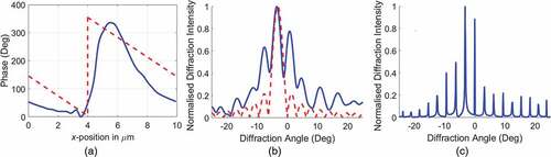
shows the resultant-phase distribution in the output plane, extracted just above the top surface of the LC layer. The far-field diffraction pattern of a single cell is shown in (b) and the diffraction pattern of an array of 100 cells in (c). These results indicate that just with two electrodes the basic blazed grating shape can be approximated, and suggest that a more versatile structure consisting of a continuous array of small, regularly spaced electrodes on the bottom surface, which could then be connected to appropriate voltages, can be used to improve the approximation or to change the period of the grating, or in general, to approximate other desired phase distributions on the top surface or output plane.
Figure 2. (Colour online) (a) Phase distribution on the top surface when a plane wave is incident normally on the bottom surface, (b) Far-field diffraction pattern of a single cell (solid blue), (c) Far-field diffraction pattern of an array of 100 cells. the dotted red lines indicate the shapes corresponding to an ideal blazed grating of the same period and total phase range.
3.1.1. Regularly spaced electrodes – ten electrode case
We consider now a section of 10 µm with 10 regularly spaced electrodes on the bottom surface of the same dimensions and spacing as those in . The voltages applied to the central electrodes are 0 and 5 V as those in and the remaining electrodes were initially set to the voltages corresponding to the potential values at the points corresponding to the centre of their position in the two-electrode structure, as the start of an iterative optimisation procedure.
A full automatic optimisation of the voltages, involving repeated use of the LC and electromagnetic modelling could be prohibitively onerous if too many iterations are needed. However, a simplified method as that used in [Citation31] can make this viable.
For this example, only a simple manual iterative procedure of successive corrections was performed, consisting of changing slightly the voltages at the electrodes in order to improve the shape of the phase distribution. Satisfactory results are achieved after only four or five iterations.
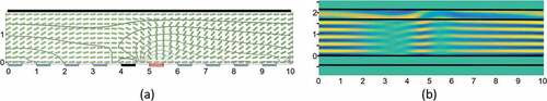
The director distribution and the magnitude of the Ex component are shown in . The two central electrodes are set at zero and 5 V as in the previous case, while the others are set as indicated in after a simple optimisation. shows the phase distribution in the output plane (top surface of the LC layer). The corresponding far-field diffraction pattern for an array of 100 cells appears in .
Figure 3. (A) (Colour online) Director distribution for the 10-electrode device. (b) Magnitude of the Ex component of the field when an x-polarised plane wave is incident normally from the bottom. the LC region is the central region shown above and is topped by small air layers and PMLs at both ends.
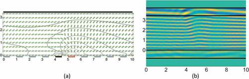
Figure 4. (Colour online) (a) Voltage pattern and values on the electrodes, (b) Ex component phase distribution on the output plane. the red dashed line indicates the shape corresponding to an ideal blazed grating of the same period and phase range, (c) Far-field diffraction pattern of an array of 100 cells.
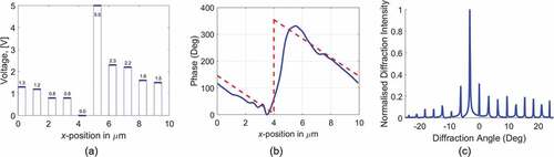
For the array of 100 cells, the diffraction efficiency for the −1 order mode is 67.8% and the ratio between the 0-order and the −1 orders of diffraction is 31.8%.
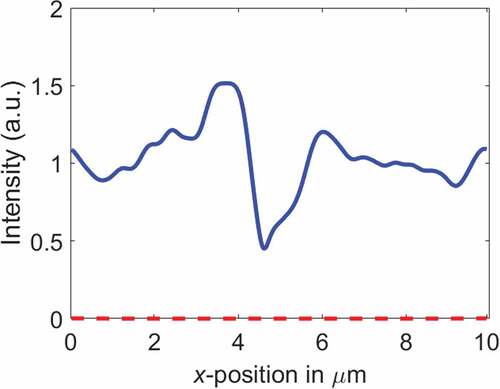
The presence of the defect causes a certain amount of twist to occur in the central region of the cell and this causes a degree of polarisation conversion, which is illustrated in . The solid line corresponds to the magnitude of the Ex component of the field when an x-polarised plane wave is used as input and the red dashed line shows the magnitude of Ey, the leaked field. This effect can be reduced substantially when a LC material with a higher value of the twist elastic constant, K22, is used. show the field component values at the output plane when the twist elastic constant is increased by a factor of 1.2 and 1.5, respectively.
Figure 5. (Colour online) (a) Amplitude distribution of the electric field components over the output plane for 5CB, Ex solid line, Ey dashed line. (b) Amplitudes if K22 is increased by a factor of 1.2. (c) Amplitudes if K22 is increased by a factor of 1.5.
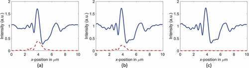
Changing the twist elastic constant in this form, the polarisation leakage is drastically reduced but there is almost no appreciable effect on the amplitude or phase distribution of the Ex component of the field or the resultant diffraction pattern.
As seen in , the amplitude of the Ex component of the field varies significantly through the cell. However, there is little effect of this variation on the far field diffraction pattern. Only a small improvement is observed if the diffraction pattern is calculated assuming a uniform amplitude distribution and this difference is because, for simplicity, the basic optimisation procedure used was looking for the best approximation to the phase response rather than the resultant diffraction pattern.
Apart from seeking a material with higher K22 to improve the performance, a higher dielectric anisotropy would be beneficial since this would lead to a thinner cell and consequently, more tolerance to variations on the incidence angle and more uniformity in the output electric field amplitude.
3.1.2. Changing the grating period
To illustrate the reconfigurabilty of this grating, the period of the structure is now reduced from 10 µm to 8 µm, comprising eight electrodes and keeping the dimensions and spacing of the electrodes unchanged. The two central electrodes are fixed at 0 and 5 V and the rest of the voltages, shown in , are found by the simple procedure of successive corrections described earlier. Again in this case, a defect pair nucleates and the −1/2 defect migrates to the middle of the cell allowing the overall abrupt change in the director orientations at either side.
Figure 6. (Colour online) (a) Voltage values on the electrodes. (b) Phase distribution of the Ex component of the field on the top surface. (c) Far-field diffraction pattern of an array of 100 cells. Dashed line indicates the shape corresponding to an ideal blazed grating of the same period and phase range.
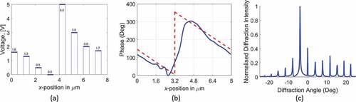
The results are shown in . The deflection angle of the −1 diffraction order increases from 3.16° to 3.96°, with a diffraction efficiency for the −1 order mode of 63.5% and a 0-order to −1 order ratio of 41% for an array of 100 cells.
The phase distribution over the output plane, , and also the diffraction pattern, , depart from the ideal a bit more than what is observed in the ten electrode case, but this is expected since less elements are used to approximate the ideal response.
3.2. Reflection case
A common and convenient form of implementation of devices like those described above is using LCOS technology. In this case, the device operates in reflection, the excitation is from above and the bottom electrodes are directly connected to the CMOS layer. As a difference to the standard LCOS devices, where the pixel electrodes are themselves the reflector, in this case, a separate reflection layer would be required.
Considering this configuration, the structure chosen is 10 µm wide by 1.7 µm tall and is filled with 5CB, the same LC material as in the structure used in transmission. The cell gap has been adjusted to have approximately phase range.
The top surface of the LC layer is covered by a continuous ground electrode and the bottom surface has an array of electrodes of the same dimensions and spacing as before. One electrode, marked with the red outline in , is connected to 3 V, other (solid black) is connected to ground and the rest, shown in grey, are set to voltages found with the iterative procedure described before, starting from the potential distribution originated by the two central electrodes. Again in this case, just a few iterations are needed to improve considerably the phase distribution and the corresponding diffraction pattern.
Figure 7. (Colour online) (a) Director distribution and equipotential lines over the LC cell when 3 V are applied to one of the bottom central electrodes (marked with red outline) and other is grounded (solid black); the rest of the voltages are chosen to approximate the ideal phase distribution (grey). (b) Magnitude of Ex component when a downwards propagating plane wave is normally incident on the top surface of the LC layer and reflected at z = 0. Dimensions are in microns; xz-plane shown.
The resultant stationary director distribution is shown in , where the −1/2 defect has already reached the final position near the top of the cell. To study the light propagation through the cell, the model is extended adding an air region at the top and terminating the structure above with a PML. At the bottom of the LC layer, a reflective layer is modelled as a dielectric with large negative imaginary permittivity (a value of 10,000 was used here). shows the distribution of the Ex component of the field over the cross-section when a plane wave propagating downwards is incident at z = 1.7 µm. An air layer and a PML were added at the bottom but this is not really necessary since the reflector at z = 0 practically stops all transmission through. The output-phase distribution, shown in , is extracted at a position in the top-air gap, just above the excitation plane at z = 1.7 µm.
Figure 8. (Colour online) (a) Voltages on the electrodes. (b) Phase distribution of the Ex component of the field on the top surface. the red line indicates the phase corresponding to an ideal blazed grating of the same period and phase range. (c) Far-field diffraction pattern of an array of 100 cells.
The phase distribution over the output plane in the air region, slightly above z = 1.7 µm and the corresponding diffraction pattern are shown in . The resultant diffraction efficiency for the −1 order mode is 76.4% and the 0-order to −1 order ratio is 6.6%. The amplitude of the output field varies in a similar way as in the transmission case using the parameters for 5CB, but with a slightly reduced total variation as shown in . However, the thinner cell does not permit twist to occur as easily as in the transmission case and the leakage to the y-polarisation is negligible, even with the low value of K22 of 5CB.
Figure 9. (Colour online) Amplitude distribution of the electric field components over the output plane for 5CB in reflection cell, Ex solid line, Ey dashed line.
The amplitude variation over the output plane is no impediment to achieve a good far field response as shown by the diffraction pattern in . This is achieved here with a grating period of 10 µm with 10 electrodes per period. As with conventional LCOS gratings, less electrodes per period are possible, but with a reduction in the fidelity of the phase response, as shown earlier.
Conventional LCOS SLM pixels are limited in size due to the strong fringing field effects at small pitch. With a typical small size pixel of about 4 µm, a grating with 10 levels would have a period of 40 µm while with the proposed structure the period would only be 10 µm long, resulting in larger deflection angles. At the same time, while in a conventional LCOS device, the fly-back region would be of the order of 4 µm to 5 µm for the same phase range [Citation32], the fly-back region of the structure described above is only of 1.1 µm.
4. Conclusions
A procedure to model accurately the optical behaviour of LC cells has been presented. It combines in this implementation, an accurate LC modelling method, which is particularly suitable to study structures containing defects and small features, with an efficient electromagnetic solver based on a FDFD formulation of the electromagnetic problem. This leads to a matrix problem that is solved using GMRes. Electromagnetic problems of this type are usually ill-conditioned and this is here treated for a 2D implementation with a modified form of a sweeping preconditioner.
The electromagnetic solver requires the values of the dielectric permittivity in each of the nodes of the FD grid and these are supplied by the LC model.
Using the same strategy followed by this procedure, a less computer-demanding constant-order LC solver, based on the Oseen-Frank formulation, can be substituted here to study problems where order variation can be neglected, as, for example, in microwave and terahertz LC devices, where diffraction effects are important but LC order variation is not.
To illustrate the capability of the method, a 2D case of a reconfigurable LC grating is proposed and analysed. It is shown that a structure consisting of a number of regularly spaced small electrodes can be configured into a periodic array where the electrode voltages are selected to shape a desired phase distribution on the output plane. In this case, this is shown for a blazed grating where a LC defect is utilised to produce the abrupt phase profile. Good results are shown for 5CB, a common LC material but not particularly suitable for this application. It is also shown that a careful choice of material can lead to thinner cells and lower polarisation leakage. Optimisation of the structure is also possible and even with a simple procedure results can be improved substantially in a few iterations.
Built in this form and using LC defects to produce the abrupt fly-back, the period of the grating can be drastically reduced compared with the standard implementation of LC gratings with LCOS SLMs, designed to approximate uniform levels of amplitude and phase over each pixel.
Disclosure statement
No potential conflict of interest was reported by the author(s).
References
- Chen H-W, Lee J-H, Lin B-Y, et al. Liquid crystal display and organic light-emitting diode display: present status and future perspectives. Light Sci Appl. 2018;7:17168.
- Pivnenko M, Li K, Chu D. Sub-millisecond switching of multi-level liquid crystal on silicon spatial light modulators for increased information bandwidth. Opt Express. 2021;29(16):24614.
- Collings N, Davey T, Christmas J, et al. The applications and technology of phase-only liquid crystal on silicon devices. J Display Technol. 2011;7(3):112–119. DOI:10.1109/JDT.2010.2049337
- Wang M, Zong L, Mao L, et al. LCOS SLM study and its application in wavelength selective switch. Photonics. 2017;4(4):22. DOI:10.3390/photonics4020022
- Robertson B, Yang H, Redmond MM, et al. Demonstration of multi-casting in a 1 × 9 LCOS wavelength selective switch. J Lightwave Technol. 2014;32(3):402–410. DOI:10.1109/JLT.2013.2293919
- Li L, Zhang R, Zhao Z, et al. High-capacity free-space optical communications between a ground transmitter and a ground receiver via a UAV using multiplexing of multiple orbital-angular-momentum beams. Sci Rep. 2017;7(1):17427. DOI:10.1038/s41598-017-17580-y
- Willner AE, Liu C. Perspective on using multiple orbital-angular-momentum beams for enhanced capacity in free-space optical communication links. Nanophotonics. 2020;10(1):435.
- Li L, Shi S, Kim J, et al. Color-selective geometric-phase lenses for focusing and imaging based on liquid crystal polymer films. Opt Express. 2022;30(2):2487–2502. DOI:10.1364/OE.444578
- Chen P, Wei B-Y, Hu W, et al. Liquid-crystal-mediated geometric phase: from transmissive to broadband reflective planar optics. Adv Matter. 2022;32:1903665.
- He Z, Yin K, Wu S-T. Miniature planar telescopes for efficient, wide-angle, high-precision beam steering. Light Sci Appl. 2021;10:134.
- Li Y. High-precision beam angle expander based on polymeric liquid crystal polarization lenses for LiDAR applications. Crystals. 2022;12:349.
- Yin K, He Z, Xiong J, et al. Virtual reality and augmented reality displays: advances and future perspectives. J Phys Photonics. 2021;3:022010.
- Deo P, Mirshekar-Syahkal D, Seddon L, et al. Microstrip device for broadband (15-65 GHz) measurement of dielectric properties of nematic liquid crystals. IEEE Trans Microw Theory Tech. 2015;63(4):1388–1398. DOI:10.1109/TMTT.2015.2407328
- Deo P, Mirshekar-Syahkal D, Seddon L, et al. Beam steering 60 GHz slot antenna array using liquid crystal phase shifter. Proceedings of the 8th European Conference on Antenna and Propagation EuCAP 2014; 2014 Apr 6–11; The Hague (The Nederlands). p. 1005–1007.
- Li J, Chu D. Liquid crystal-based enclosed coplanar waveguide phase shifter for 54–66 GHz applications. Crystals. 2019;9(12):650.
- Reese R, Jost M, Polat E, et al. A millimeter-wave beam-steering lens antenna with reconfigurable aperture using liquid crystal. IEEE Trans Antennas Propag. 2019;67(8):5313–5324. DOI:10.1109/TAP.2019.2918474
- Sasaki T, Asano T, Sakamoto M, et al. Subwavelength liquid crystal gratings for polarization-independent phase shifts in the terahertz spectral range. Opt Mater Express. 2020;10(2):240–248. DOI:10.1364/OME.10.000240
- James R, Willman E, Fernández FA, et al. Finite-element modeling of liquid-crystal hydrodynamics with a variable degree of order. IEEE Trans Electron Devices. 2006;53(7):1575–1582. DOI:10.1109/TED.2006.876039
- Willman E, Fernández FA, James R, et al. Modeling of weak anisotropic anchoring of nematic liquid crystals in the Landau-de Gennes theory. IEEE Trans Electron Devices. 2007;54(10):2630–2637. DOI:10.1109/TED.2007.904369
- James R, Willman E, Fernández FA, et al. Computer modeling of liquid crystal hydrodynamics. IEEE Trans Magn. 2008;44(6):814–817. DOI:10.1109/TMAG.2007.916029
- Engquist B, Ying L. Sweeping preconditioner for the Helmholtz equation: moving perfectly matched layers. Multiscale Model Simul. 2011;9:686–710.
- Merewether DE, Fisher R, Smith FW. On implementing a numeric Huygens’s source scheme in a finite difference program to illuminate scattering bodies. IEEE Trans Nucl Sci. 1980;27(6):1829–1833.
- Umashankar KR, Taflove A. A novel method to analyze electromagnetic scattering of complex objects. IEEE Trans Electromagn Compat. 1982;24(4):397–405.
- Taflove A, Hagness SC. Computational electrodynamics. 3rd ed. Boston (MA): Artech House; 2005.
- Rumpf RC. Simple implementation of arbitrarily shaped total-field/scattered-field regions in finite-difference frequency-domain. Prog Electromagn Res B. 2012;36:221–248.
- Rumpf RC, Garcia CR, Berry EA, et al. Finite-Difference frequency-domain algorithm for modeling electromagnetic scattering from general anisotropic objects. Prog Electromagn Res B. 2014;61:55–67.
- Zola RS, Bisoyi HK, Wang H, et al. Dynamic control of light direction enabled by stimuli-responsive liquid crystal gratings. J Adv Mater. 2019;31:1806172.
- Habibpourmoghadam A, Wolfram L, Jahanbakhsh F, et al. Tunable diffraction gratings in copolymer network liquid crystals driven with interdigitated electrodes. ACS Appl Electron Mater. 2019;1:2574–2584.
- James R, Gardner MC, Fernández FA, et al. 3D modelling of high resolution devices. Mol Cryst Liq Cryst. 2006;450:105–305.
- James R, Fernández FA, Day SE, et al. Modeling of the diffraction efficiency and polarization sensitivity for a liquid crystal 2D spatial light modulator for reconfigurable beam steering. J Opt Soc Am A. 2007;24(8):2464–2473. DOI:10.1364/JOSAA.24.002464
- Georgiou AG, Komarčević M, Wilkinson TD, et al. Hologram optimisation using liquid crystal modelling. Mol Cryst Liq Cryst. 2005;434:183–511.
- Lu T, Pivnenko M, Robertson B, et al. Pixel-Level fringing-effect model to describe the phase profile and diffraction efficiency of a liquid crystal on silicon device. Appl Opt. 2015;54(19):5903–5910. DOI:10.1364/AO.54.005903
- De Gennes PG, Prost J. The physics of liquid crystals. Oxford (UK): Oxford University Press; 1993.
- Willman EJ. Three dimensional finite element modelling of liquid crystal electro-hydrodynamics [ dissertation]. London (UK): University College London; 2008.
- Willman EJ, Seddon L, Osman M, et al. Liquid crystal alignment induced by micron-scale patterned surfaces. Phys Rev E. 2014;89(5):052501. DOI:10.1103/PhysRevE.89.052501
- Sonnet AM, Virga EG. Dynamics of dissipative ordered fluids. Phys Rev E. 2001;64:031705.
- Sonnet AM, Maffettone PL, Virga EG. Continuum theory for liquid crystals with tensorial order. J Non-Newtonian Fluid Mech. 2004;119:51–59.
- Qian T, Sheng P. Generalized hydrodynamic equations for nematic liquid crystals. Phys Rev E. 1998;58(6):7475–7485.
- Albani M, Bernardi P. A numerical method based on the discretization of Maxwell equations in integral form. IEEE Trans Microw Theory Tech. 1974;22(4):446–450.
- Champagne NJ, Berryman JG, Hm B. FDFD: a 3D Finite-difference frequency-domain code for electromagnetic induction tomography. J Comput Phys. 2001;170:830–848.
- Yang M, Day SE, Fernández FA. (Poster 75): modelling the optics of high resolution liquid crystal devices by the finite differences in the frequency domain method. Proceeding of the International Workshop on Electromagnetics (iWEM 2017); 2017 May 30–June 1; London. p. 141–143.
- Yang M, Nie Z, Day SE, et al. (Poster P3): accurate modelling of the optics of high resolution liquid crystal devices including diffractive effects. Abstracts of BLCS, The British Liquid Crystal Society Annual Conference; 2018 Mar 26–28; Manchester (UK). p. P3.
- Chew WC, Weedon WH. A 3D perfectly matched medium from modified Maxwell’s equations with stretched coordinates. Microw Opt Technol Lett. 1994;7:599–604.
- Rappaport CM. Perfectly matched absorbing boundary conditions based on anisotropic lossy mapping of space. IEEE Microwave Guided Wave Lett. 1995;5:90–92.
- Mittra R, Pekel U. A new look at the perfectly matched layer (PML) concept for the reflectionless absorption of electromagnetic waves. IEEE Microwave Guided Wave Lett. 1995;5:84–86.
- Sacks Z, Kingsland D, Lee R, et al. A perfectly matched anisotropic absorber for use as an absorbing boundary condition. IEEE Trans Antennas Propag. 1995;43:1460–1463.
- Shin W, Fan S. Choice of the perfectly matched layer boundary condition for frequency-domain Maxwell’s equations solvers. J Comput Phys. 2012;231:3406–3431.
- Kitson SC, Geisow A. Bistable alignment of nematic liquid crystals around microscopic posts. Mol Cryst Liq Cryst. 2004;412:153–161.
- Willman EJ, Fernández FA, James R, et al. Switching dynamics of a post aligned bistable liquid crystal device. IEEE/OSA J Display Technol. 2008;4(3):276–281. DOI:10.1109/JDT.2008.921780
- Bryan-Brown GP, Wood EL, Brown CV, et al. Grating aligned bistable nematic device. SID Symp Dig Tech Pap. 1997;28:37–40.
- Jones JC. 40.1: invited paper: the Zenithal bistable device: from concept to consumer. SID Symp Dig Tech Pap. 2007;38(1):1347–1350.
- Parry-Jones LA, Elston SJ. Flexoelectric switching in a zenithally bistable nematic device. J Appl Phys. 2005;97:093515.
- Jones SA, Day SE, Fernández FA, et al. Defect dynamics of bistable latching. Abstracts of BLCS-2019, the British Liquid Crystal Society Annual Conference; 2019 Apr 15–17; Leeds (UK).
- Cummins PG, Dunmur DA, Laidler DA. The dielectric properties of Nematic 44′ n -pentylcyanobiphenyI. Mol Cryst Liq Cryst. 1975;30:109–123.
- James R, Willman E, Ghannam R, et al. Hydrodynamics of fringing-field induced defects in nematic liquid crystals. J Appl Phys. 2021;130:134701.