
 ?Mathematical formulae have been encoded as MathML and are displayed in this HTML version using MathJax in order to improve their display. Uncheck the box to turn MathJax off. This feature requires Javascript. Click on a formula to zoom.
ABSTRACT
In this paper, we have investigated the dielectric properties of nematic liquid crystals (NLCs) by measuring the resonant frequencies of inverted microstrip lines (IMSLs) of NLC being the substrate material at the microwave frequency band. The designed IMSL devices consist of a cavity for NLC mixture between the inverted microstrip line and the ground plane. The anisotropy values of the NLCs were determined by observing the change of the resonant frequency when the strength of external electric fields applied on the NLCs varied. The experiments demonstrated that the effective dielectric constant of the NLC can be manipulated by the proposed devices via external bias voltage for tuning. The accuracy of the method for determining the dielectric constants of JC-M-LC-E7 (JC-E7) and QYPD-036 LCs was analysed with several prototypes based on two separate designs. The high accuracy of 91% in permittivity determination was demonstrated, and the design and fabrication techniques are beneficial for making microwave components of high tunability.
Graphical abstract
1. Introduction
Nematic liquid crystals (NLCs) provide many unique characteristics in microwave and millimetre-wave (mmW) applications. Liquid crystals (LCs) have been extensively used to develop high-performance components and devices in the visible region of the spectrum while it is becoming increasingly important to be used for tunable devices in millimetre-wave applications [Citation1]. It was reported that the NLCs have been used in 5G mmW systems [Citation2,Citation3] and terahertz (THz) wave systems. At mmW frequency band, LC materials have been used for tunable filters [Citation4–9], phase shifters [Citation10–13] and steerable antennas [Citation14]. Moreover, a great number of THz devices based on LCs have been proposed. These include phase shifters [Citation15,Citation16], modulators [Citation17], absorbers [Citation18], optical switches [Citation19] and filters [Citation20].
Liquid crystals with anisotropic characteristics are used in mmW communication systems to make tunable devices adaptive to the varying propagation conditions. Hence, they can be used to realise smart antenna solutions. One of the critical challenges to achieve agility at mmW communication through conventional technologies is that the tunable devices for this function consume a lot of power. lists the amount of power consumed by the antenna array using different phase shift technologies. For example, considering silicon-based technology, in [Citation21], a silicon-based array operating at 28 GHz consumes 20 W for an effective isotropic radiated power (EIRP) of about 50 dBm. As for the microwave liquid crystal (MLC)-based technology, in [Citation22], the same operating frequency and EIRP were used to realise the MLC-based
array, with the power consumption of less than 5.5 W. In another design with the array size of
, the power consumption of MLC-based technology is also significantly less than that of silicon-based technology. Compared with some conventional devices, the power consumption of liquid crystals decreases with increasing frequency in the RF domain. So the liquid crystal phase shifter can effectively reduce power consumption at higher frequencies. Power consumption is one of the most critical parameters for implementing phased antenna arrays, and hence, a liquid crystal-based phase shift technology provides a clear advantage over silicon based.
Table 1. Power consumption of active arrays using different phase shift technologies.
Liquid crystals for optical applications (displays, lenses, etc.) have been studied extensively [Citation23]. The molecules’ orientation of liquid crystal can be changed with the strength of an external electric field or magnetic field, thereby altering their permittivity [Citation24]. The liquid crystal has the performances of an extended, structurally rigid, anisotropic shape in the most liquid crystalline systems, allowing a great number of materials to exhibit liquid crystalline behaviour [Citation25]. The birefringence is one of the important physico-chemical properties of liquid crystals, and this property can extend to microwave frequencies and be used to make tunable devices at millimetre or THz frequency band [Citation26].
The dielectric properties of LC can be controlled by applying external electric or magnetic fields. However, it is very important to optimise their performance by anchoring the LC molecules at the initial state. Many of the devices relied on traditional alignment methods developed in the past for optical purposes. But these techniques for optical applications can lead to problems such as corrosion in microwave devices as the indium tin oxide (ITO) conduction layers are replaced by more active copper, which is coated with polyimide (PI) and curing at high temperature [Citation27]. The curing process accelerates copper oxidation (during the alignment agent baking process at 230°C for 30 min). The process of deposition and treatment of the PI needs to be improved to mitigate the negative effects accompanied with the initial alignment layer.
According to its alignment tendency towards the orientation of the external electric fields, NLC can be classified into two types: (1) positive or p-type, when in which the molecules align parallel to the applied electric field; (2) negative or n-type, where
, in which the molecules align perpendicular to the applied field [Citation28]. The dielectric anisotropy of the LC is measured by
, where
and
are the parallel and perpendicular parts of the dielectric constant for the LC, respectively.
By employing the anisotropy property of NLC, the orientation of NLC molecules can be controlled by external fields to obtain a desired effective dielectric constant for tuning. When no bias was applied, molecules of LC are parallel to the metal floor induced by the alignment of the PI film. In this case, the effective dielectric constant is defined as . When the bias voltage
exceeds the threshold voltage
(
), the resonant frequency starts to change and the effective dielectric constant also increases. Meanwhile, the orientation of LC molecules can be gradually deflected, and the long axis of LC molecules becomes parallel to the external field in the patch area. At this point, the applied voltage reaches the saturation voltage (
=
), where the effective relative permittivity is equal to the maximum value
[Citation29]. Thus, we can get intermediate dielectric constant values with the intermediate voltage values (
) [Citation30].
It is very important to measure the effective dielectric constant accurately for the LC to be used. summarises different measurement methods of liquid crystals across the 5–40 GHz range, and it also gives the relative dielectric anisotropy () and measurement error on permittivity for different LC mixtures. In [Citation31–33], the permittivity characteristics of LCs can be determined by using the resonant technique, which offers high sensitivity and accurate results for effective dielectric constants, but the resonant method has a weakness of being appropriate for individual frequency. In [Citation34], a broadband coaxial transmission line method is used to characterise LCs between 360 MHz and 23 GHz. Even though the broadband method can determine the dielectric constants of LCs over a wide range of frequencies, it offers a relatively low accuracy. The method in [Citation35] proposes a planar transmission line for the characterisation of the NLC in the 60 GHz band. One of the advantages of this method is that the structure allows the application of the bias field to the LC through the strips. However, this method achieves lower accuracy than the ones based on resonator. In [Citation36], a microstrip line method is used to obtain the permittivity of the LCs. For this purpose, a unique LC cell is formed, and the measurements are based on the inverted microstrip line through applying the bias voltage to the LC cell using a bias tee. A metamaterial absorber has been used at 90–120 GHz for LC characterisation in [Citation37].
Table 2. The common measurement techniques to characterise LCs.
In this paper, we present a method to measure the effective relative permittivities of NLCs using an inverted microstrip line (IMSL) structure. Two designs were developed for this purpose; initially, in Design 1, as the inverted microstrip line was connected with the coplanar waveguide (CPW) for measurement connection, only bias voltages of 20 V() were applied on it to protect the vector network analyser (VNA). In Design 2, the microstrip line was separated from the CPWs, hence, a higher voltage of 32 V(
) can be applied. The effective relative permittivities of two NLCs, QYPD-036 and JC-M-LC-E7 (JC-E7), were determined by acquiring the resonant frequency from measurement and fitting the response by varying dielectric constant of the substrate material in simulation.
2. Materials and methods
It is critically important to know the properties of the materials precisely before using them in devices at millimetre or THz frequency band. The NLCs (catalogue number: JC-M-LC-E7 from JCOPTIX, and QYPD-036 from Qingdao QY Liquid Crystal Co., Ltd.) were commercially available off-the-shelf, and they both have been developed primarily for optical applications and show a birefringence property equivalent to E7, and their dielectric properties at the visible light spectrum are summarised in . They can also be employed in microwave and mmW applications. The chemical structure of QYPD-036 LC monomer is illustrated in . Their dielectric characteristics at the microwave frequency band were investigated in this study.
Figure 1. The chemical structure of the LC monomer, QYPD-036.
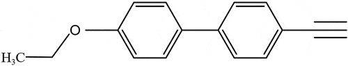
Table 3. The comparison of the recently available NLCs and the classical display mixtures E7 (Merck) for display and photonic applications.
The threshold voltage differs for the two types of LC mixtures, which can be expressed as follows [Citation30]:
by finding the corresponding parameters of the LC QYPD-036, the splay elastic constant is 27.0 pN, and the anisotropy at 1 kHz,
, is 13.4. Hence, the value of the threshold voltage is approximately 1.524 V. In terms of JC-M-LC-E7, it has a similar property as E7 where
= 10.8 pN, and
= 0.915 V.
In order to estimate the relative dielectric constant of the LC, the control over the orientation of LC molecules must be realised, and this is normally achieved by applying external electric fields varying with the voltage between two electrodes in conjuncture with pre-alignment mechanism of anchoring. To align LC molecules along a well-defined orientation, two anchoring surfaces are created on the opposite sides of the container for LC. The creation of this alignment layer for initial anchoring is done in three main steps: (1) the deposition of polyimide with a spin coating technique; (2) the curing of the polymer, heat up to 230°C for half an hour; and (3) make the microscopic grooves on the polymer surface through rubbing along the desired direction of the long molecule axis for initial anchoring, and a velvet cloth can be used for this step. With a proper rotation speed for coating, the thin layer of polyimide film for alignment is typically 50–100 nm in thickness.
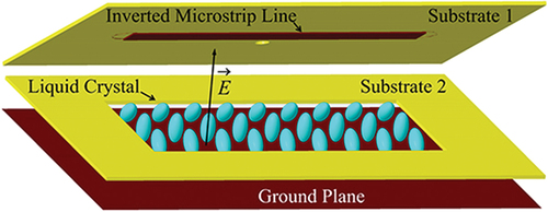
Inverted microstrip line by using LC as the substrate was developed; in this way, the electric fields can be created by applying a bias voltage source between the microstrip line and the ground plane, with pre-aligned LC between them. The dielectric characteristics of the LCs can be tuned by electric fields controlled through varying the bias voltage between the IMSL and the ground plane. The IMSL design for measurement of the relative permittivity of NLCs is shown in . The IMSL structure consists of two substrate layers, which are defined as Substrate 1 and Substrate 2, respectively. A sealed cavity is obtained on the middle layer by cutting on Substrate 2. At each of its ends, the inverted microstrip line is connected through a via to a CPW. At the interface between Substrate 1 and Substrate 2, there is an LC-filling hole for injection and a conductor patch. The bottom layer is the ground plane, and the LC layer is effectively sandwiched between the IMSL and the ground plane. In , the inverted microstrip line can be seen on the bottom surface of Substrate 1, and LC molecules in the cavity were deflected by an applied electric field. Both the bottom surface of Substrate 1 and the top surface of the ground plane were spin-coated with a thin passivation layer of PI to improve the planarity of the surfaces.
Figure 2. (Colour online) Design 1 of an NLC-based IMSL: on Substrate 1, the inverted microstrip line and the CPW for measurement are on two sides of the board, and they are connected through a via. Substrate 2 is to provide a cavity in the middle board to contain the NLC mixture, and the bottom board is working as a metallic ground plane.
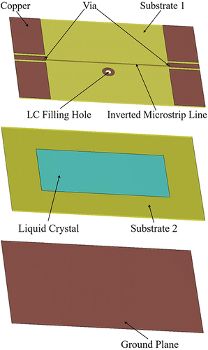
Figure 3. (Colour online) The inverted microwstrip line, NLC in the cavity and the electric fields of the waves propagating through.
Compared to the first design, the second structure is different where the feed-line is not connected with the microstrip line so that a higher voltage can be applied on the microstrip line without a risk to damage the instrument for measurements. The dimensions of the IMSL devices are indicated in ; based on the way of connection between the CPW feed-line and inverted microstrip line, two designs were introduced, where Design 1 is shown as case 1, and Design 2 is case 2 as illustrated in . In case 1, vias are used for connection, while coupling capacitors are used in case 2. Moreover, the parameters of two IMSL devices are listed in .
Figure 4. (Colour online) The detailed dimensions of the IMSL designs: case 1 refers to the vias used in Design 1, and case 2 refers to the coupling mechanism employed in Design 2.
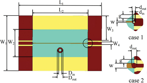
Table 4. The dimensions of the two IMSL designs in millimetres.
The IMSL device was fabricated using a standard photolithography process. For Design 1, the fabrication process was based on the substrate of commercially available Rogers Duroid. Both the top and middle layers, fabricated from RO4350B, have a thickness of 0.254 mm (as shown in , a = 0.254 mm for Substrate 1, b = 0.254 mm for Substrate 2) and an effective dielectric constant of = 3.66. Moreover, a uniform surface of approximately 100 nm was deposited by spin coating PI on the bottom surface of Substrate 1, and the microgrooves were created by rubbing unidirectionally along the short edge direction of the substrate. The ground plane was fabricated from a 30 mm
20 mm
1 mm slab of copper sheet and was dealt with in the same deposition and rubbing processes. In the measurement, the frequency response of LC samples was measured using VNA (Keysight N9918A) with the function waveform signal generator to provide 1 KHz sine wave signal as a voltage source. The material used for the substrate of Design 2 is F4BMX. Design 2 has the same thickness of each layer as Design 1. In Design 2, the dielectric permittivity of the top layer is
= 2.2, while the middle layer has an effective dielectric constant of
= 3.
Figure 5. Cross section of the inverted microstrip line structure under two scenarios: (a) the empty cavity and (b) the cavity was filled with LCs.
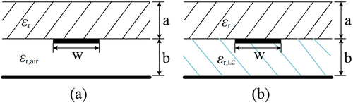
The relationship between the dielectric constant of the material in the cavity and the resonant frequency of the device is described as follows. When the cavity is empty, the value of the effective dielectric constant () can be calculated by [Citation8]
where the relative permittivity of the air is = 1, and
the functions can be expressed by
where coefficients are defined in terms of
(see Appendix A).
When the cavity is filled with LCs, the effective dielectric constant can be calculated with [Citation38]
where
Due to fringing effects, the IMSL appears longer than the physical length. Thus, the normalised extension of the length can be expressed as [Citation39]
so the resonant frequency of the IMSL device is given by
where the light of speed is , and the effective length of the IMSL becomes
and a factor for the effective length calculation, , is different under the two scenarios. It is summarised in for the two IMSL designs.
Table 5. The factor to calculate the effective length of IMSLs under the two scenarios.
The resonant frequency can be calculated from the half-power frequencies
and
of the IMSL device [Citation40]
and quality factor [Citation40]
the loss tangent has the following relation with the quality factor [Citation41]
With the quality factor acquired through simulations or measurements for the devices, the loss tangent can then be determined by the unloaded quality factor.
3. Measurement results
3.1. Result analysis
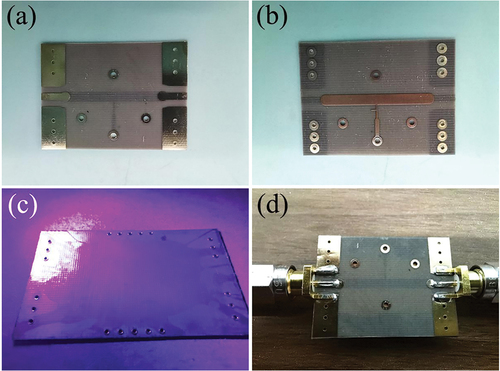
shows the fabrication process of the prototype for Design 1, where both substrate 1 and PI alignment layers are presented before final assembly. The PI film for alignment is clearly seen in the picture. The bias voltage has been applied on the IMSL device through a coaxial cable which is shown in . In , both sides of the first layer for Design 2 are shown before assembling process, and a thin PI pre-alignment layer was spin-coated onto the top surface of the ground plane. The IMSL device was connected to the VNA through SMA connectors.
Figure 6. (Colour online) Fabrication process of the IMSL device based on Design 1: (a) top view of Substrate 1, (b) bottom view of Substrate 1, (c) the top surface of the board of ground plane was spin-coated with a thin layer of PI and (d) the bias voltage being applied on an IMSL device based on Design 1.
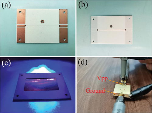
Figure 7. (Colour online) Fabrication process of the IMSL devices based on Design 2: (a) top view of Substrate 1, (b) bottom view of Substrate 1, (c) the top surface of the board of ground plane was spin-coated with a thin layer of PI and (d) a completed IMSL device based on Design 2.
lists the measurement of relative permittivity of the JC-M-LC-E7 LC. In the unbiased state (0 V), the LC molecules are aligned in the default direction, the perpendicular polarisation state = 2.18. At
= 20 V, the majority of LC molecules are parallel to microwave electric field, and the quasi-parallel permittivity
= 2.62 was derived. Hence, the tunable range of the relative dieletric anisotropy of the NLC is
= 0.44. The perpendicular permittivity is less than the quasi-parallel permittivity represented by the two corresponding resonant frequencies, resulting in a positive dielectric anisotropy. The values of the effective relative permittivity of the QYPD-036 LC are listed in .
Table 6. The dielectric properties of the JC-M-LC-E7 LC determined based on the measurements of the IMSL devices.
Table 7. The dielectric properties of the QYPD-036 LC determined based on the measurements of the IMSL devices.
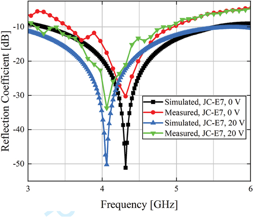
For Design 1, the frequency response of the empty resonator, i.e. no LC was filled in the IMSL device, was first measured. We obtained the simulated results from a full-wave simulator. Scattering parameters are the measurements related to transmission and incident waves from devices under testing, and reflection coefficient is defined as the ratio of reflected wave voltage to incident wave voltage. The measured and simulated frequency responses are compared in . It is noted that there is a good agreement between the measured and the simulated values of the resonant frequencies. The deviation between the magnitudes of simulation and measurement in is possibly due to the manufacturing defects during assembly of the feeding ports. depicts the measured reflection coefficient when different bias voltages were applied, while the liquid crystal was filled inside the cavity. It shows that frequency responses based on the simulation were very close to the measured results. A clear shift in the resonant frequency is observed in the measured responses, indicating that effective dielectric constant of the LC has been changed with increasing bias voltages.
Figure 8. (Colour online) The comparison of scattering parameter of the empty IMSL device (Design 1, air in the cavity) between simulation and measurement.
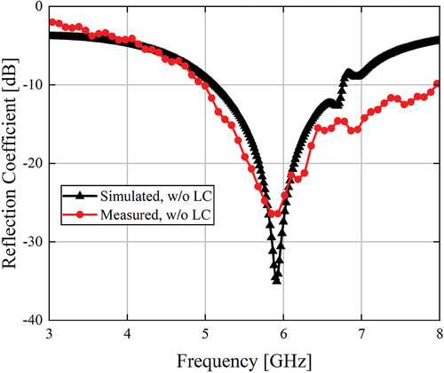
Figure 9. (Colour online) Simulated and measured scattering parameters of the IMSL device (Design 1) with JC-M-LC-E7 being filled in the cavity, under 0 and 20 V () bias voltage applied, respectively.
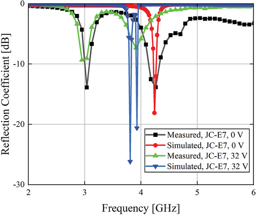
For Design 2, the comparison between the simulated and measured resonant frequencies of the empty device is presented in . It indicated that the results from the measurements are in good agreement with that of the simulations. The simulated results and the measured results of Design 2 with JC-M-LC-E7 filled are presented in . It revealed that as the bias voltage increased from 0 to 32 V(), the resonant frequency of the device shifts from 4.25 GHz to 3.92 GHz. Meanwhile, with an excursion of resonant frequency, the determined effective relative permittivity is moving from 2.17 to 2.82.
Figure 10. (Colour online) The comparison of scattering parameter of the empty IMSL device (Design 2, air in the cavity) between simulation and measurement.
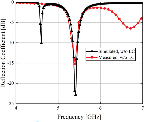
Figure 11. (Colour online) Simulated and measured scattering parameters of IMSL device (Design 2) with JC-M-LC-E7 LC being filled in the cavity, under 0 and 32 V () bias voltage applied, respectively.
3.2. Uncertainty and reliability analysis
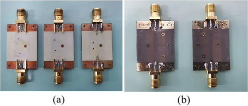
The method to characterise dielectric constants of LCs by employing resonant devices can produce results with a high performance. However, the accuracy level achieved from the method is heavily dependent on tolerance of manufacturing. Hence, two different designs and several devices under test (DUT) (see ) were manufactured for uncertainty and reliability analyses.
Figure 12. (Colour online) Fabricated NLC-based IMSL devices: (a) the three devices based on Design 1 and (b) the two devices based on Design 2.
shows the discrepancies of resonant frequencies between measurement and simulation based on Design 1. For Design 1, the DUT 2 and the DUT 3 show a small uncertainty of 7% and 4% on the dielectric anisotropy, respectively, while the DUT 1 has a maximum deviation of 12%, where the shift of the resonant frequency is 0.2 GHz from 5.9 GHz (). The differences between the resonant frequencies of two devices of Design 2 are presented in . For Design 2, the DUT 1 has a maximum uncertainty of 14% on the dielectric anisotropy, where the deviation of the resonant frequency is 0.17 GHz from the designed frequency of 5.4 GHz (). The main reason for uncertainty may be from tolerance of manufacturing and fabrication.
Figure 13. (Colour online) The difference between the measured and simulated results of resonant frequency for the empty DUTs (the Design 1 of IMSL, air in the cavity).
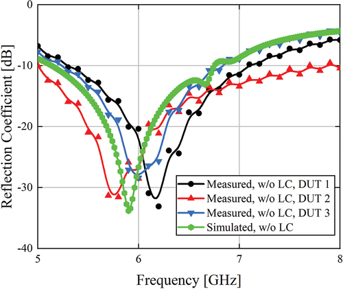
Figure 14. (Colour online) The difference between the measured and simulated results of resonant frequency for the empty DUTs (the Design 2 of IMSL, air in the cavity).
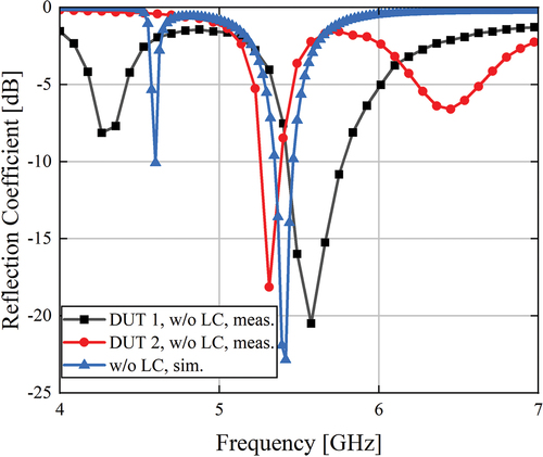
Table 8. The uncertainty analysis based on the IMSL devices of Design 1.
Table 9. The uncertainty analysis based on the IMSL devices of Design 2.
4. Discussion
IMSL devices have been designed and measured to characterise NLCs as a substrate material. The dielectric characteristics of the NLC can be tuned by the electric fields applied on it. The and
of JC-M-LC-E7 determined from the method were 2.17 and 2.82, respectively, based on Design 2, which was obtained with a maximum voltage of 32 V(
). It demonstrated a high performance of this mixture. The determined
and
of QYPD-036 were 2.24 and 2.95, which was in an agreement with the results reported in the literature. A smaller dielectric anisotropy was observed possibly due to the lower bias voltage applied.
The thin PI pre-alignment layer is in particular effective for thin planar structures where the thickness of LC layer is typically less than 150 . However, due to the manufacturing capacity and tolerance, the thickness of the LC layer in the prototypes is 254
for both designs, some LC molecules particularly at the regions away from the centre of the microstrip line are likely not in complete parallel to the surface of PI alignment layers due to reduced anchoring force, consequently mitigating the orientation effectiveness. Hence, the effectiveness of the LC’s tunability can be compromised by the actual physical properties of the alignment layers – thickness, orientation and depth of the grooves obtained through mechanical rubbing.
5. Conclusion
In this paper, inverted microstrip line devices with tunability for determining effective relative permittivities of NLCs have been presented. This method was used to determine the dielectric constants of the two types of NLCs, JC-M-LC-E7, QYPD-036, over the frequency range of 2–8 GHz. The resonant frequencies of two designs have been used to determine the effective dielectric constants of NLCs. To the best of the author’s knowledge, this is the first study to report the relative permittivity of JC-M-LC-E7 LC at the microwave frequency band. The dielectric anisotropies of the NLC mixtures were obtained by interpolating the relative permittivities of substrate material of two IMSL designs between measurements and simulations. Several devices were fabricated and measured to confirm the reliability of the obtained results. Moreover, it was shown in the measurement results that the resonant frequency point was very sharp. Therefore, the sensitivity of the measurements was high and so was its accuracy. The design method can be extended to characterise NLCs at other mmW or THz bands.
Disclosure statement
No potential conflict of interest was reported by the authors.
Correction Statement
This article has been corrected with minor changes. These changes do not impact the academic content of the article.
Additional information
Funding
References
- Polat E, Tesmer H, Reese R, et al. Reconfigurable millimeter-wave components based on liquid crystal technology for smart applications. Crystals. 2020;10(5):346. DOI:10.3390/cryst10050346
- Jakoby R, Gaebler A, Weickhmann C. Microwave liquid crystal enabling technology for electronically steerable antennas in SATCOM and 5G millimeter-wave systems. Crystals. 2020;10(6):514.
- Maune H. Microwave liquid crystal technology. Crystals. 2020;10(8):716.
- Jiang D, Li X, Fu Z, et al. Millimeter-wave broadband tunable band-pass filter based on liquid crystal materials. IEEE Access. 2020;8:1339–1346.
- Yazdanpanahi M, Mirshekar-Syahkal D. Millimeter-wave liquid-crystal-based tunable bandpass filter. In: Proceedings of the 2012 IEEE Radio and Wireless Symposium; 2012 Jan 5–18. Santa Clara (CA): IEEE; 2012. p. 139–142.
- Prasetiadi AE, Karabey OH, Weickhmann C, et al. Continuously tunable substrate integrated waveguide bandpass filter in liquid crystal technology with magnetic biasing. Electron Lett. 2015;51(20):1584–1585.
- Kaesser T, Fritzsch C, Franz M. Tunable RF filters based on liquid crystal for space applications. Crystals. 2020;10(6):455.
- Jiang D, Liu Y, Li X, et al. Tunable microwave bandpass filters with complementary split ring resonator and liquid crystal materials. IEEE Access. 2019;7:126265–126272.
- Polat E, Reese R, Jost M, et al. Tunable liquid crystal filter in nonradiative dielectric waveguide technology at 60 GHz. IEEE Microw Wirel Compon Lett. 2019;29(1):44–46.
- Li JF. Rethinking figure-of-merits of liquid crystals shielded coplanar waveguide phase shifters at 60 GHz. Crystals. 2021;4:444–451.
- Li JF, Chu DP. Liquid crystal-Based enclosed coplanar waveguide phase shifter for 54–66 GHz applications. Crystals. 2019;9(12):650.
- Tesmer H, Razzouk R, Polat E, et al. Temperature characterization of liquid crystal dielectric image line phase shifter for millimeter-wave applications. Crystals. 2021;11(1):63. DOI:10.3390/cryst11010063
- Li JF. Bias tees integrated liquid crystals inverted microstrip phase shifter for phased array feeds. In: Proceedings of the 2020 21st International Conference on Electronic Packaging Technology (ICEPT). Guangzhou, China; 2020 Aug 12–15; 2020 (IEEE). p. 1–5.
- Reese R, Polat E, Tesmer H, et al. Liquid crystal based dielectric waveguide phase shifters for phased arrays at W-band. IEEE Access. 2019;7:127032–127041.
- Qiu QL, Yu XP, Sui WQ. A K-band low-power phase shifter based on injection locked oscillator in 0.13 µm CMOS technology. J Infr Millim Terahertz Waves. 2017;38(11):1368–1386.
- Han Z, Ohno S, Tokizane Y, et al. Thin terahertz-wave phase shifter by flexible film metamaterial with high transmission. Opt Express. 2017;25(25):31186–31195.
- Wang J, Tian H, Wang Y, et al. Liquid crystal terahertz modulator with plasmon-induced transparency metamaterial. Opt Express. 2018;26(5):5769–5776.
- Wang L, Ge S, Hu W, et al. Graphene-assisted high-efficiency liquid crystal tunable terahertz metamaterial absorber. Opt Express. 2017;25(20):23873–23879.
- Zhang L, Fan YX, Liu H, et al. Hypersensitive and tunable terahertz wave switch based on non-bragg structures filled with liquid crystals. J Light Technol. 2017;35(14):3092–3098.
- Zhang LH, Li JJ, Bao YH, et al. A broad stop-band filter based on multilayer metamaterials in the THz regime. J Infr Millim Waves. 2016;35(3):267–270.
- Anokiwaves Inc. Introduction to all silicon millimeter-wave 5G arrays. Microwave Journal; 2019 [cited 2020 June 5]. Available from: https://www.microwavejournal.com/articles/31937-introduction-to-all-silicon-millimeter-wave-5g-arrays
- ALCAN Systems, Dehghani MR. ALCAN’s smart antenna’s 5G opportunities and solutions. 2019 [cited 2020 June 5]. Available from: https://www.alcansystems.com/alcans-smart-antennas-5g-opportunities-and-solutions/
- Yeh P. Optics of liquid crystal displays. In: Proceedings of the 2007 Conference on Lasers and Electro-Optics; 2007 Aug 26–31; Pacific Rim, Seoul. Korea (South): IEEE; 2007. p. 1–1.
- Sun SY, Yu X, Wang PJ, et al. Electronically tunable liquid-crystal-based f-band phase shifter. IEEE Access. 2020;8:151065–151071.
- DiLisi GA. An introduction to liquid crystals. San Rafael (CA): Morgan & Claypool; 2019. p. 2053–2571.
- Yang F, Sambles JR. Determination of the microwave permittivities of nematic liquid crystals using a single-metallic slit technique. Appl Phys Lett. 2002;81(11):2047–2049.
- Nobles JE, Melnyk O, Glushchenko A, et al. Effect of alignment methods on liquid crystal performance in millimeter wave devices. Eng Res Exp. 2020;2(2):025002. DOI:10.1088/2631-8695/ab82ec
- Kawamoto H. The history of liquid-crystal displays. Proceedings of the IEEE. In: ; 2002. 2002;90(4). p. 460–500.
- Fritzsch C, Wittek M. Recent developments in liquid crystals for microwave applications. In: Proceedings of the 2017 IEEE International Symposium on Antennas and Propagation & USNC/URSI National Radio Science Meeting; 2017 July 9–14. SanDiego (CA): IEEE; 2017. p. 1217–1218.
- Nova V, Bachiller C, Villacampa B, et al. Characterization of nematic liquid crystals at microwave frequencies. Crystals. 2020;10(12):1106. DOI:10.3390/cryst10121106
- Sánchez JR, Nova V, Bachiller C. Characterization of nematic liquid crystal at microwave frequencies using split-cylinder resonator method. IEEE Trans Microw Theory Tech. 2019;67(7):2812–2820.
- Schaub DE, Oliver DR. A circular patch resonator for the measurement of microwave permittivity of nematic liquid crystal. IEEE Trans Microw Theory Tech. 2011;59(7):1855–1862.
- Yazdanpanahi M, Bulja S, Mirshekar-Syahkal D, et al. Measurement of dielectric constants of nematic liquid crystals at mm-wave frequencies using patch resonator. IEEE Trans Instrum Meas. 2010;59(12):3079–3085.
- Mueller S, Penirschke A, Dam C, et al. Broad-band microwave characterization of ilquid crystals using a temperature-controlled coaxial transmission line. IEEE Trans Microw Theory Tech. 2005;53(6):1937–1945.
- Bulja S, Mirshekar-Syahkal D, James R, et al. Planar transmission line method for measurement of dielectric constants of liquid crystals in 60 GHz band. In: Proceedings of the 2009 Asia Pacific Microwave Conference; 2009 Dec 7–10. Singapore: IEEE; 2009. p. 341–344.
- Bulja S, Mirshekar-Syahkal D, James R, et al. Measurement of dielectric properties of nematic liquid crystals at millimeter wavelength. IEEE Trans Microw Theory Tech. 2010;58(12):3493–3501.
- Lu HB, Jing SC, Xia TY, et al. Measurement of LC dielectric constant at lower terahertz region based on metamaterial absorber. IEICE Electron Express. 2017;14(12):2017046.
- Tomar RS, Bhartia P. New quasi-static models for the computer aided design of suspended and inverted microstrip lines. IEEE Trans Microw Theory Technol. 1987;35(4):453–457.
- Hammerstad EO. Equations for microstrip circuit design. In: Proceedings of 1975 5th European Microwave Conference; 1975 Sept 1–4. Hamburg (Germany): IEEE; 1975. p. 268–272.
- Abrie PLD. Design of RF and microwave amplifiers and oscillators. 2nd ed. Norwood (MA): Artech House; 2009. p. ch. 4.
- Balanis CA. Antenna theory. 3rd ed. Hoboken (NJ): Wiley; 2005. p. ch. 14.
Appendix A.
Expression for 
Defining
we have