Abstract
It has been experimentally confirmed in many chemical vapor deposition (CVD) processes that charged nanoparticles tend to be generated in the gas phase. In an effort to confirm and measure charged gas phase nuclei, that might be generated during the deposition of Si thin films by hot wire CVD, we performed an in-situ measurement using particle beam mass spectrometer (PBMS), which can measure a size distribution of nanoparticles at low pressure. The size distribution of positively and negatively charged Si gas phase nuclei generated during hot wire CVD under 1.5 torr could be firstly measured. The particle diameter at the peak of the size distribution is about 10 ∼ 13 nm. At a wire temperature of 1800°C, the number concentration of negatively charged Si nanoparticles was higher than that of positively charged ones. The size and number concentration of charged nanoparticles decreased with increasing wire temperature from 1800 to 2000°C and increased with increasing SiH4 concentration from 3 to 6%.
Copyright 2013 American Association for Aerosol Research
1. INTRODUCTION
Hot wire or catalytic chemical vapor deposition (HWCVD or cat-CVD) of Si has been studied for a few decades because of their unique advantages over other CVD systems such as crystalline film deposition at low substrate temperature, high deposition rate, and high gas utilization (Wiesmann et al. Citation1979; Matsumura Citation1991; Nelson et al. Citation2001; Iwaniczko et al. Citation2003). Especially, the deposition of nanocrystalline silicon thin films at low temperature has attracted great attention as potential applications for thin film solar cells (Schropp Citation2004) and transistors (Stannowski et al. Citation2003). However, it has not been clearly understood why nanocrystalline Si thin films can be deposited at the substrate temperature even below 500°C during HWCVD. The diffusion of silicon is so low below 500°C that the amorphous silicon should be formed at such a low temperature.
In order to explain the low temperature deposition of crystalline silicon during HWCVD, Hwang and coworkers (Kim et al. Citation2006; Lee et al. Citation2008a,Citationb) suggested that the low temperature deposition of crystalline silicon during HWCVD can be explained if it is assumed that crystalline Si gas phase nuclei are formed in the high temperature region near the hot wires and incorporated into the growing surface at low substrate temperature. To confirm the generation of crystalline gas phase nuclei, Lee et al. (Citation2008a) extracted the gas phase nuclei from the HWCVD reactor. They captured the hypothetical Si nanoparticles on a transmission electron microscopy (TEM) grid membrane placed at room temperature and observed the crystalline silicon nanoparticles. They also showed that the gas phase nuclei are electrically charged. Based on the fact that the gas phase nuclei are charged, Lee et al. (Citation2008b) applied the substrate bias, which resulted in the increase of the growth rate of Si films. In addition, Park et al. (Citation2009, Citation2010) showed that the electric field generated around the hot wires depended markedly on whether the power supply is DC or AC and affected the spatial distribution of charged nanoparticles in the chamber as well as the deposition behavior during HWCVD of Si.
In the plasma CVD, the charged gas phase nuclei often grow into a visible size. Therefore, it is well known that charged nanoparticles are suspended during plasma CVD, which is called “dusty plasma” (Roca i Cabarrocas Citation2002). Cabarrocas suggested that this silane plasma can be incorporated into films and produce the so-called “polymorphous structure.” Ostrikov (Citation2005) made an extensive review on the incorporation of gas phase nuclei into nanostructures for a reactive-plasma-assisted nanoassembly process and indicated the importance of detection and control for a building block. Takamura et al. (Citation1997) found that nanoparticles having size in the range of 1 ∼ 9 nm are formed in the gas phase and then deposited as the main component of the deposition flux during a thermal plasma process.
Although all of mentioned facts support the possibility that charged gas phase nuclei might be formed during HWCVD, there has been no in-situ measurement of charged nuclei generated in the gas phase during the HWCVD. Adachi et al. (Citation1992, Citation1993, Citation1995, Citation1996, Citation2000) and Hwang and coworkers (Kim et al. Citation2009a,Citationb, Citation2010a,Citationb, Citation2012) could measure the size distribution of charged nanoparticles generated during atmospheric CVD of many systems using a differential mobility analyzer (DMA) combined with a Faraday cup electrometer. The measurements of nanoparticles in the range of 1∼50 nm are very difficult especially when the CVD reactor is under low pressure. Therefore, we are motivated to use the particle beam mass spectrometer (PBMS), which appears to be ideal for measurement of nanoparticles generated in the low-pressure CVD process. The purpose of this study is to confirm charged Si gas phase nuclei and to measure their size distribution during HWCVD of Si using the PBMS. The PBMS measurements showed that the wire temperature and the silane concentration affected the size distribution of charged Si nanoparticles.
2. EXPERIMENT
Si thin films were deposited on a glass substrate (eagle 2000XG, 25 × 25 × 0.7 mm3) by HWCVD. The detail about the HWCVD reactor is explained in the supporting information 1 in the online supplemental information. The hydrogen-diluted silane gas 30%SiH4–70%H2 was supplied as reactants. The flow rates of 30% SiH4–70%H2 and H2 were 18 and 91 sccm, respectively, which produced a gas mixture of 5%SiH4–95%H2. The Si films were deposited at wire temperatures of 1800, 1900, and 2000°C for 20 min under 1.5 torr. A substrate was fixed as 4 cm below the hot wires. For wire temperatures of 1800, 1900, and 2000°C, the substrate temperatures were, respectively, 370, 430, and 470°C. In addition, the Si films were deposited at SiH4 concentrations of 3, 4, 5, and 6%, for which the flow rates of 30%SiH4–70%H2 were 10, 14, 18, and 23 sccm with 91 sccm H2, respectively. The deposition rate of Si films was determined from the cross-sectional microstructure using field emission scanning electron microscopy (FESEM, JSM-6330F, JEOL, Japan).
To measure the size distribution of charged Si nanoparticles generated in the gas phase, the PBMS was used under the same condition as the Si thin films deposition. In general, Si films are deposited at reactor pressure below 0.5 torr in HWCVD process. However, the PBMS measurements in this study were carried out at 1.5 torr due to two reasons, which are explained in the supporting information 2. shows the schematic of the PBMS installed to the exhaust line of the HWCVD reactor. The line connected between the exhaust of the HWCVD reactor and the PBMS inlet was short and straight, which turned out to be critical in minimizing the diffusion loss of charged nanoparticles. All of the apparatus were electrically grounded to minimize the space charge effect. The reactor pressure was controlled by a throttle valve at the exhaust line.
FIG. 1 Schematic of experimental set-up for in-situ measurement of charged nanoparticles generated in the gas phase during the HWCVD process. (Color figure available online.)
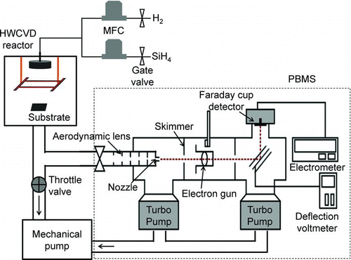
In the present study, an artificial charger was not used because nanoparticles generated in the gas phase are spontaneously charged in the HWCVD reactor. The electric charge of nanoparticles was assumed plus-minus 1, considering a soft charging condition in the HWCVD process. The reliability of our assumption was examined in Figure S1 and PBMS DATA INVERSION section in the supporting information 3. The charged nanoparticles were classified by an electrostatic deflector which deflects charged nanoparticles in proportion to the ratio of the kinetic energy to charge by the induced critical deflection voltage (Kim et al. Citation2002).
3. RESULTS AND DISCUSSION
shows photographs and cross-sectional FESEM images of Si thin films deposited for 20 min at wire temperatures of 1800, 1900, and 2000°C, respectively, with a 5% SiH4 concentration under 1.5 torr. At a wire temperature of 1800°C, an appreciable amount of Si was deposited with the color being yellowish as shown in . The film thickness of was about 1.3 μm, as shown in . The black dashed line represents the boundary between the glass substrate and the Si film. As the wire temperature increased, Si thin films were hardly deposited as shown in and , which did not differ appreciably from a bare glass substrate. As also shown in and , the cross-sectional FESEM images of and showed that the Si deposition had hardly occurred. This result shows that the deposition behavior of Si thin films is drastically affected by wire temperatures.
FIG. 2 Photographs and corresponding cross-sectional FESEM images of Si thin films deposited for 20 min on the glass substrate at wire temperatures of (a), (d) 1800°C, (b), (e) 1900°C, and (c), (f) 2000°C under 1.5 torr with a flowing gas mixture of 5%SiH4–95%H2. The dashed line represents the boundary between the substrate and the film. (Color figure available online.)
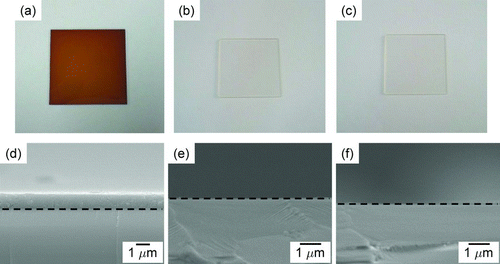
FIG. 3 Plane view FESEM images of Si films deposited for 20 min at wire temperatures of (a) 1800°C, (b) 1900°C, and (c) 2000°C under the condition of .
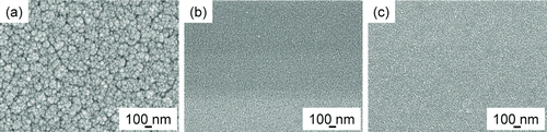
shows the FESEM images of the surface morphology of Si thin films in . for a wire temperature of 1800°C showed a typical microstructure of Si thin films deposited by HWCVD. On the other hand, in and , continuous films were not formed; instead, the Si nanoparticles smaller than 20 nm were densely deposited on the surface of films. This result indicated that the deposition rate was decreased markedly at wire temperatures above 1900°C under the examined experimental conditions.
This result is contrary to the general observation during the typical HWCVD process. In general, the deposition rate of Si films is increased with increasing wire temperature in the HWCVD process (Heintze et al. Citation1996; Gogoi et al. Citation2011) because the decomposition efficiency of the reactants increases with increasing wire temperature. Such a difference in the dependence of the wire temperature on deposition is believed to come from the difference in the reactor pressure; the working pressure is less than 0.5 torr in the general HWCVD process whereas it is 1.5 torr in the current experiment.
The high reactor pressure would increase the amount of atomic hydrogen, which would increase the etching rate. In preliminary experiments, we confirmed that the deposition of Si films occurred at the reactor pressure below 0.5 torr but did not occur above 0.6 up to 2 torr at the wire temperature of 2000°C. It is widely known that an appreciable amount of atomic hydrogen is generated by HWCVD and the atomic hydrogen etches silicon (Wanka and Schubert Citation1997). Moreover, they reported that the etching rate of Si increased with increasing wire temperature in HWCVD. Besides, Hickmott (Citation1960) reported that the amount of atomic hydrogen increased with increasing reactor pressure in HWCVD.
FIG. 4 TEM images of Si nanoparticles captured for 10 s on a TEM grid membrane at the same condition as the Si films deposition under (a) 0.3 torr and (b) 1.5 torr.
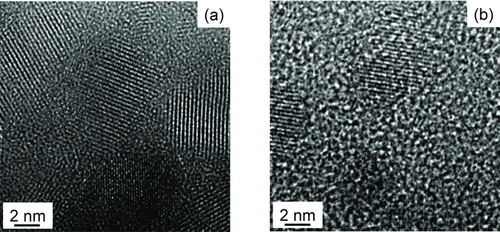
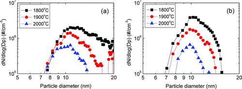
FIG. 5 The size distribution of (a) positively and (b) negatively charged Si nanoparticles generated in the gas phase at various wire temperatures with a flowing gas mixture of 5%SiH4–95%H2 under 1.5 torr. (Color figure available online.)
These reports implied that the amount of atomic hydrogen would increase with increasing wire temperature and pressure. Based on this implication, results of and can be analyzed. At wire temperatures of 1900 and 2000°C, a sufficient amount of atomic hydrogen would be generated and the Si etching rate would be high enough so that the deposition would hardly occur as shown in , , , and whereas at the wire temperature of 1800°C, the amount of atomic hydrogen would not be sufficiently large and the Si etching rate would not be high enough. As a result appreciable Si deposition would occur as shown in and .
shows the TEM images of Si nanoparticles captured for 10 sec on a TEM grid membrane at the same condition as the Si film deposition, respectively, at 0.3 and 1.5 torr. Both and showed that the Si nanoparticles had crystalline lattices. Moreover, in the Raman analysis, the crystalline fraction of Si film deposited under 1.5 torr was higher than that under 0.3 torr as shown in Figure S2. Since at the substrate temperature of 370°C, the diffusivity of Si would be negligibly small, these crystalline Si nanoparticles are expected to have formed in the gas phase near the hot wires and to have landed on the substrate rather than to have nucleated on the substrate by surface diffusion. This suggestion is supported from the experimental confirmation of the extensive gas phase nucleation by the PBMS measurements as will be shown in and .
FIG. 6 Cross-sectional FESEM images of Si films deposited for 20 min at SiH4 concentrations of (a) 3%, (b) 4%, (c) 5%, and (d) 6% with a wire temperature of 1800°C under 1.5 torr. The dashed line represents the boundary between the substrate and the film.
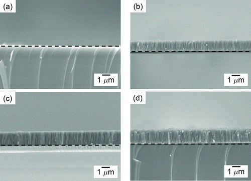
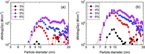
FIG. 7 The size distribution of (a) positively and (b) negatively charged Si nanoparticles generated in the gas phase at various SiH4 concentrations with a wire temperature of 1800°C under 1.5 torr. (Color figure available online.)
shows the size distribution of charged nanoparticles measured by the PBMS during the deposition of Si thin films at various wire temperatures under the same deposition conditions of and . Both positively and negatively charged nanoparticles were generated. The size distribution of positively charged nanoparticles was broader than that of negatively charged ones. As the wire temperature increased, the number concentration of both positively and negatively charged nanoparticles decreased drastically. The particle diameter at the peak of the size distribution is about 10 ∼ 13 nm. The peak diameters of both positively and negatively charged nanoparticles slightly decreased with increasing wire temperature. At the wire temperature of 1800°C, the number concentration of peak diameter for negatively charged nanoparticles was 2 times higher than that of positively charged ones. As the wire temperature was increased, the number concentration at the peak diameter was nearly the same for both positively and negatively charged nanoparticles. These results indicate that the generation and growth of charged nanoparticles in the gas phase are suppressed with increasing wire temperature.
The nucleation of charged Si nanoparticles must have occurred in the gas phase through the decomposition of SiH4. At wire temperatures of 1900 and 2000°C, the decomposition efficiency would be higher than that at 1800°C. As a result, a larger amount of Si precipitation is expected at the wire temperatures of 1900 and 2000°C than that at 1800°C. However, shows that the number concentration of charged nanoparticles decreased with increasing wire temperature. This result can be explained if we assume that the Si–H system has a retrograde solubility where the solubility of silicon in the gas phase increases with decreasing temperature. In this case, the amount of precipitation of solid Si in the gas phase decreases with decreasing temperature. In addition, etching of solid Si would depend on the amount of atomic hydrogen. The amount of atomic hydrogen produced by hot wires would increase with increasing wire temperature. Therefore, the size and number concentration of the Si gas phase nuclei would decrease with increasing wire temperature as shown in . It should be noted that at the wire temperature above 1900°C, where the Si thin film was hardly deposited, the number concentration of nanoparticles at the peak diameter was drastically decreased to below 2 × 106 cm−3.
shows the FESEM images of the cross-sections of Si thin films at various SiH4 concentrations. The films were deposited for 20 min with SiH4 concentration being varied from 3 to 6% at a wire temperature of 1800°C under 1.5 torr. At 3% SiH4, the Si film was hardly deposited as shown in . As the SiH4 concentration increased, the amount of the deposited Si film increased and the deposition rate was proportional to the SiH4 concentration. The average film thicknesses at 4, 5, and 6% SiH4 were, respectively, 1.1, 1.3, and 1.6 μm. The increased deposition rate with increasing SiH4 concentration would be related with the increased amount of Si precipitation.
shows the size distribution of positively and negatively charged Si nanoparticles measured by the PBMS under the same conditions as that of . The peak diameter and number concentration of both positively and negatively charged Si nanoparticles increased with increasing SiH4 concentration. The number concentration of negatively charged Si nanoparticles was higher than that of positively charged ones. At 3% SiH4, where the deposition rate was negligible, the number concentrations of both positively and negatively charged nanoparticles were very low. This result implies that the nucleation and growth of charged nanoparticles in the gas phase are enhanced with increasing SiH4 concentration.
and clearly show that charged nanoparticles are generated in the gas phase during the deposition of Si thin films and their size distribution showed the multiple modes in the range of large particle size. The details about the origin of multiple modes are explained in the supporting information 4. As to the mechanism for the generation of charged nanoparticles in the gas phase during HWCVD of Si, the origin of negative charges would be electrons thermally emitted from the hot wires and those electrons would provide the sites for charge-induced nucleation (Roca i Cabarrocas Citation2002; Ostrikov Citation2005). The origin of positive charges would be the positive surface ionization (Langmuir and Kingdon Citation1925) of atoms or molecules such as H or SixHy on the hot wires. The details are explained by the supporting information 5. However, further theoretical and experimental studies are needed to understand the charging mechanism more clearly in the HWCVD process.
Although this study shows that charged nanoparticles are generated under the conditions of Si films deposition, their role in the growth of Si film is not known. It is not yet certain whether the charged nanoparticles are mainly involved, partly involved or hardly involved in the deposition of Si films. However, in our previous studies (Kim et al. Citation2006; Lee et al. Citation2008a,Citationb; Park et al. Citation2009, Citation2010; Hwang and Lee Citation2010), the film growth rate, crystallinity, and microstructural evolution of Si films were affected by both substrate bias and wire bias during the HWCVD process. Furthermore, the experiments herein show that the deposition rate of Si films was impractically low under conditions where the generation of charged nanoparticles was suppressed and was increased with increasing number concentration of charged Si nanoparticles. These results imply that the charged Si nanoparticles might be involved in the Si film growth. More systematic work is required to clarify the role of charged Si nanoparticles.
4. CONCLUSION
This is the first report on in-situ measurements of charged Si nanoparticles generated under the low-pressure deposition of Si thin films by HWCVD. The positively and negatively charged Si nanoparticles were generated during the deposition of Si thin films. The particle diameter of charged Si nanoparticles was about 10 ∼ 13 nm. Their size distribution was affected by wire temperature and silane concentration. As the wire temperature increased, the number concentration of both positively and negatively charged Si nanoparticles was decreased. The peak diameter and the number concentration were increased with increasing SiH4 concentration. The deposition rate of Si thin films was increased with increasing number concentration of charged Si nanoparticles.
uast_a_725959_sup_28809033.zip
Download Zip (412.3 KB)uast_a_725959_sup_28547595.zip
Download Zip (413.8 KB)Acknowledgments
This work was supported by the Brain Korea (BK21) program, Republic of Korea.
[Supplementary materials are available for this article. Go to the publisher's online edition of Aerosol Science and Technology to view the free supplementary files.]
REFERENCES
- Adachi , M. , Okuyama , K. , Fujimoto , T. , Satoh , J. and Muroyama , M. 1996 . Morphology Control of Films Formed by Atmospheric-Pressure Chemical Vapor Deposition Using Tetraethylorthosilicate/Ozone System . Jap. J. Appl. Phys. , 35 : 4438 – 4443 .
- Adachi , M. , Fujimoto , T. , Itoh , Y. and Okuyama , K. 2000 . Numerical Simulations of Films Formed by Cluster/Particle Co-Deposition in Atmospheric-Pressure Chemical Vapor Deposition Process Using Organic Silicon Vapors and Ozone Gas . Jap. J. Appl. Phys. , 39 : 3542 – 3548 .
- Adachi , M. , Okuyama , K. and Tohge , N. 1995 . Particle Generation and Film Formation in an Atmospheric-Pressure Chemical Vapour Deposition Process using Tetraethylorthosilicate . J. Mater. Sci. , 30 : 932 – 937 .
- Adachi , M. , Okuyama , K. , Tohge , N. , Shimada , M. , Satoh , J. and Muroyama , M. 1992 . Gas-Phase Nucleation in an Atmospheric Pressure Chemical Vapor Deposition Process for SiO2 Films using Tetraethylorthosilicate (TEOS) . Jap. J. Appl. Phys. , 31 : L1439 – L1422 .
- Adachi , M. , Okuyama , K. , Tohge , N. , Shimada , M. , Satoh , J. and Muroyama , M. 1993 . Particle Generation and Film Formation in an Atmospheric-Pressure Chemical Vapor Deposition Reactor Using the Tetraethylorthosilicate (TEOS)/He, TEOS/O2/He, and TEOS/O3/He Systems . Jap. J. Appl. Phys. , 32 : L748 – L751 .
- Gogoi , P. , Jha , H. S. and Agarwal , P. 2011 . Variation of Microstructure and Transport Properties with Filament Temperature of HWCVD Prepared Silicon Thin Films . Thin Solid Films , 519 : 4506 – 4510 .
- Heintze , M. , Zedlitz , R. , Wanka , H. N. and Schubert , M. B. 1996 . Amorphous and Microcrystalline Silicon by Hot Wire Chemical Vapor Deposition . J. Appl. Phys. , 79 : 2699 – 2706 .
- Hickmott , T. W. 1960 . Interaction of Hydrogen with Tungsten . J. Chem. Phys. , 32 : 810 – 823 .
- Hwang , N. M. and Lee , D. K. 2010 . Charged Nanoparticles in Thin Film and Nanostructure Growth by Chemical Vapour Deposition . J. Phys. D:Appl. Phys. , 43 : 483001 – 483038 .
- Iwaniczko , E. , Xu , Y. , Schropp , R. E. I. and Mahan , A. H. 2003 . Microcrystalline Silicon for Solar Cells Deposited at High Rates by Hot-Wire CVD . Thin Solid Films , 430 : 212 – 215 .
- Kim , C. S. , Chung , Y. B. , Youn , W. K. and Hwang , N. M. 2009a . Generation of Charged Nanoparticles during the Synthesis of ZnO Nanowires . Aerosol Sci. Technol. , 43 : 120 – 125 .
- Kim , C. S. , Chung , Y. B. , Youn , W. K. and Hwang , N. M. 2009b . Generation of Charged Nanoparticles during the Synthesis of Carbon Nanotubes by Chemical Vapor Deposition . Carbon , 47 : 2511 – 2518 .
- Kim , J. Y. , Kim , D. Y. and Hwang , N. M. 2006 . Spontaneous Generation of Negatively Charged Clusters and Their Deposition as Crystalline Films during Hot-Wire Silicon Chemical Vapor Deposition . Pure Appl. Chem. , 78 : 1715 – 1722 .
- Kim , C. S. , Youn , W. K. and Hwang , N. M. 2010a . Generation of Charged nanoparticles and Their Deposition during the Synthesis of Silicon Thin Films by Chemical Vapor Deposition . J. Appl. Phys. , 108 : 014313-1–014313-6
- Kim , C. S. , Kwak , I. J. , Choi , K. J. , Park , J. G. and Hwang , N. M. 2010b . Generation of Charged Nanoparticles during the Synthesis of Silicon Nanowires by Chemical Vapor Deposition . J. Phys. Chem. C , 114 : 3390 – 3395 .
- Kim , T. , Suh , S. M. , Girshcik , S. L. , Zachariah , M. R. and McMurry , P. H. 2002 . Particle Formation during Low-Pressure Chemical Vapor Deposition from Silane and Oxygen: Measurement, Modeling, and Folm Properties . J. Vac. Sci. Technol. , 20 : 413 – 423 .
- Langmuir , I. and Kingdon , K. H. 1925 . Thermionic Effects Caused by Vapours of Alkali Metals . Proc. R. Soc. London, Ser. A , 107 : 61 – 79 .
- Lee , D. K. , Chung , Y. B. , Kim , J. K. and Hwang , N. M. 2008b . Effects of the Electric Bias on the Deposition Behavior of Silicon Films on Glass during Hot-Wire Chemical Vapor Deposition . J. Cryst. Growth , 310 : 4368 – 4372 .
- Lee , S. S. , Kim , C. S. and Hwang , N. M. 2012 . Generation of Charged Nanoparticles during the Synthesis of GaN Nanostructures by Atmospheric Pressure Chemical Vapor Deposition . Aerosol Sci. Technol. , 46 : 1100 – 1108 .
- Lee , S. S. , Ko , M. S. , Kim , C. S. and Hwang , N. M. 2008a . Gas Phase Nucleation of Crystalline Silicon and Their Role in Low-Temperature Deposition of Microcrystalline Films during Hot-Wire Chemical Vapor Deposition . J. Cryst. Growth , 310 : 3659 – 3662 .
- Matsumura , H. 1991 . Formation of Polysilicon Films by Catalytic CVD Method . Jpn. J. Appl. Phys. , 30 : 1522 – 1524 .
- Nelson , B. P. , Iwaniczko , E. , Mahan , A. H. , Wang , Q. , Xu , Y. Crandall , R. S. 2001 . High-deposition Rate a-Si:H n-i-p Solar Cells Grown by HWCVD . Thin Solid Films , 395 : 292 – 297 .
- Ostrikov , K. 2005 . Colloquium: Reactive Plasmas as a Versatile Nanofabrication Tool . Rev. Mod. Phys. , 77 : 489 – 511 .
- Park , S. Y. , You , S. J. , Kim , C. S. and Hwang , N. M . 2010 . Comparison of Charge Generation from Hot Wires Between AC and DC Power Supply and Its Effect on Deposition Behavior during Hot-Wire Chemical Vapor Deposition of Silicon . J. Cryst. Growth , 312 : 2459 – 2464 .
- Park , S. Y. , Yang , S. M. , Kim , C. S. and Hwang , N. M. 2009 . Effect of Bias Applied to Hot Wires on Generation of Positive and Negative Charges during Silicon Hot-Wire Chemical Vapor Deposition . J. Phys. Chem. C , 113 : 17011 – 17017 .
- Roca i Cabarrocas , P. 2002 . Plasma Enhanced Chemical Vapor Deposition of Silicon Thin Films for Large Area Electronics . Curr. Opin. Solid State Mater. Sci. , 6 : 439 – 444 .
- Schropp , R. E. I. 2004 . Present Status of Micro- and Polycrystalline Silicon Solar Cells Made by Hot-Wire Chemical Vapor Deposition . Thin Solid Films , 451–452 : 455 – 465 .
- Stannowski , B. , Rath , J. K. and Schropp , R. E. I. 2003 . Thin-film Transistors Deposited by Hot-Wire Chemical Vapor Deposition . Thin Solid Films , 430 : 220 – 225 .
- Takamura , Y. , Hayasaki , K. , Terashima , K. and Yoshida , T. 1997 . Cluster Size Measurement using Microtrench in a Thermal Plasma Flash Evaporation Process . J. Vac. Sci. Technol. B , 15 : 558 – 565 .
- Wanka , H. N. and Schubert , M. N. 1997 . High Silicon Etch Rates by Hot Filament Generated Atomic Hydrogen . J. Phys. D:Appl. Phys. , 30 : L28 – L31 .
- Wiesmann , H. , Ghosh , A. K. , McMahan , T. and Strongin , M. 1979 . A-Si:H Produced by High Temperature Thermal Decomposition of Silane . J. Appl. Phys. , 50 : 3752 – 3754 .