
Abstract
Electrosprayed nanodroplets impacting on covalently bonded materials at velocities of a few kilometers per second strongly modify their surfaces by sputtering atoms, amorphizing the region surrounding the impact, and carving craters of comparable size. This article investigates the effects of the projectile's molecular mass on the phenomenology of the impact on Si, SiC, Ge, and GaAs at impact velocities significantly higher than previously studied. An appropriate range of molecular mass is covered by electrospraying the ionic liquids ethylammonium nitrate, EAN, and 1-ethyl-3-methylimidazolium bis(trifluoromethylsulfonyl) imide, EMI-Im, which have molecular masses of 108 and 391 amu, respectively. The beamlets are characterized with the time-of-flight technique to determine the impact velocity, stagnation pressure, and molecular kinetic energy of the projectiles, and to estimate their average diameters. The ranges of these parameters are 7–17 km/s, 40–190 GPa, 50–420 eV, and 10–14 nm. Under these conditions, we find that the molecular mass has a strong effect on sputtering: the sputtering yield for the heavier EMI-Im molecule is always higher than for EAN, with maximum values for Si, SiC, Ge, and GaAs of 4.3, 11.5, 10.9, and 9.4 atoms per EMI-Im molecule, and 1.1, 3.9, 3.3, and 2.9 in the case of EAN. More importantly, droplets of the same diameter (10 nm) and kinetic energy eject significantly different numbers of atoms, with average ratios between the EMI-Im and EAN droplets of 1.8, 1.5, 1.7, and 1.5 for Si, SiC, Ge, and GaAs. Molecular dynamics simulations reproduce the observed enhancement of the sputtering at increasing molecular mass.
Copyright 2015 American Association for Aerosol Research
1. INTRODUCTION
Nanodroplets impacting on hard materials at velocities exceeding a few kilometers per second modify the surface of the targets in a variety of ways: they amorphize thin surface layers by melting the region surrounding the impact, which is followed by an ultrafast quench; they carve craters of comparable size in general, and orders of magnitude larger in the case of silicon, providing a method for texturizing the surface; and they sputter large numbers of atoms (Borrajo-Pelaez et al. Citation2013; Gamero-Castaño et al. Citation2014). Electrohydrodynamic atomization in the cone-jet mode is the source of these nanodroplets. This atomization technique is well known in the aerosol community for generating sprays with narrow diameter distributions and average diameters that can be controlled from a few nanometers to tens of microns by selecting the flow rate and the physical properties of the fluid (Cloupeau and Prunet-Foch Citation1989). In addition, electrosprayed drops are naturally charged near the Rayleigh limit (Fernandez de la Mora Citation1996), or maximum charge that a stable drop can hold, and therefore can be accelerated by an electrostatic field to the highest possible kinetic energy for a given diameter (solid particles can hold a higher net charge, but a suitable charging method has not been developed yet). These two properties make electrospray a unique particle source for beam research and applications, one that enables the investigation of a projectile size range inaccessible until now: the problem of energetic impact has traditionally been separated in two fields, the hypervelocity impact of macroprojectiles (Davison Citation2008) and the energetic impact of atomic (Sigmund Citation1969), molecular, and gas cluster ions (Yamada Citation2014). The intervening projectile diameter range, between the 3 or 4 nm of the larger gas cluster ions and the micron-sized projectiles accelerable by guns (Walsh et al. Citation1993), has remained experimentally unexplored due to the lack of a suitable projectile source. Besides the fundamental knowledge that can be gained from the study of a significantly new range of projectiles, electrosprayed nanodroplets may intensify the size-related advantages of gas cluster ions for certain surface engineering applications and for secondary mass spectrometry of large molecules. Although Mahoney et al. (Citation1991) and Mahoney (Citation1998) previously utilized droplets and clusters of glycerol as projectiles for secondary ion mass spectrometry and surface cleaning, the recently reported sputtering rates and surface modifications of materials as hard as GaN, SiC, or B4N represent a qualitative advancement of nanodroplet beams. The current development is rooted in the improved understanding of electrospraying, especially in the area of nanodroplet generation, which is largely due to the work of Fernández de la Mora and collaborators on both the physics of electrosprays (Fernández de la Mora and Loscertales Citation1994), and the use of highly conducting liquids including ionic liquids (Gamero-Castaño and Fernández de la Mora Citation2000; Garoz et al. Citation2007).
Electrosprayed nanodroplets are efficient sputtering projectiles (Gamero-Castaño and Mahadevan Citation2009a). Polycrystalline B4C and single-crystal semiconductors such as Si, GaN, SiC, Ge, GaAs, GaSb, InAs, and InP have been sputtered by nanodroplets of the ionic liquid 1-ethyl-3-methylimidazolium bis(trifluoromethylsulfonyl) imide, EMI-Im, at projectile velocities up to 7.2 km/s; the EMI-Im molecule has a kinetic energy of 105 eV at this velocity (Gamero-Castaño and Mahadevan Citation2009b; Borrajo-Pelaez et al. Citation2013). Maximum sputtering yields for these materials range between 1.9 and 4.5 substrate atoms per molecule, significantly higher than the yields of gas cluster ions. The maximum sputtering rates for the hard and inert SiC and GaN are 410 and 630 nm/min, much higher than the sputtering rates of ion beams and comparable to typical reacting ion etching rates for Si (Sugiura et al. Citation1986; Cho et al. Citation2000). Molecular dynamics simulations of the impact of EMI-Im nanodroplets on single-crystal silicon have shown that the ejection is a combination of knock-on and thermal sputtering, both driven by the initial phase of the impact characterized by intense collisionality (Saiz and Gamero-Castaño Citation2014). Finally, a study of the effect of the projectile's molecular mass on the sputtering of silicon using six different liquids covering the mass range between 45 and 773 amu has revealed an important dependence on this parameter, the larger the mass the higher the sputtering yield and the roughness of the bombarded surface at fixed impact velocity (Borrajo-Pelaez and Gamero-Castaño Citation2015). This finding suggests that nanodroplet sputtering is an atomic-scale phenomenon proceeding under non-equilibrium conditions, and which is not amenable to continuum modeling.
The present work extends the research on the effect of the molecular mass to a variety of semiconductors, and to impact velocities significantly higher than previously studied. We bombard targets of single-crystal Si, SiC, Ge, and GaAs with nanodroplets of EMI-Im and ethylammonium nitrate, EAN, whose impacts are known to have distinct effects on Si as a result of their significantly different molecular masses, 391 and 108 amu, respectively (Borrajo-Pelaez and Gamero-Castaño Citation2015). In addition, we use molecular dynamics to simulate the impacts of EMI-Im and EAN nanodroplets on Si and explain the role of the molecular mass on sputtering. The remaining of the article is organized as follows: Section 2 describes the experimental setup and methods, and the relevant properties of the beams; Section 3 introduces the molecular dynamics model; Section 4 discusses the measurements of the sputtering yield, the sputtering rate, and the roughness of the bombarded surfaces; Section 5 describes the molecular dynamics simulations and uses this information to rationalize the experimental results; and Section 6 summarizes the main findings.
2. EXPERIMENTAL SETUP AND BEAM CHARACTERIZATION
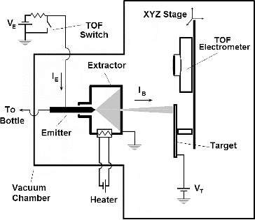
is a diagram of the experimental setup. An electrospray beam is generated inside a vacuum chamber with a base pressure of 8 × 10⁻⁶ Torr, and accelerated toward a sputtering target by an electrostatic field. The emitter is a chamfered platinum tube with a length of 1.2 cm and inner and outer diameters of 160 and 460 μm. The fluid is stored outside the chamber and fed to the emitter through a fused silica capillary. The length and inner diameter of the capillary, 31.3 cm and 40 μm, respectively, provide sufficient hydraulic resistance to drive the flow with a controllable pressure drop, typically several hundred torrs. A voltage difference VE is applied between the emitter and a grounded extracting electrode to set an electrospray in the cone-jet mode. Its magnitude is between 2 and 3 kV, while the polarity is negative for EMI-Im and positive for EAN, hence generating negatively and positively charged nanodroplets, respectively. The temperature of the electrospray emitter can be increased above room temperature using an electrical heater and a thermocouple embedded in the extractor, and connected to a digital controller. Although the current of the electrospray IE is several hundred nanoamps, a pinhole with a diameter of 0.55 mm located in the axis of the extractor reduces the amount IB that strikes the target to tens of nanoamps. We have bombarded four different single-crystal semiconductors, Si, SiC, Ge, and GaAs, all purchased from El-Cat Inc. The SiC targets are 10 × 10 × 0.43 mm hexahedrons of the 6H polytype with [0001] orientation, while the Si, Ge, and GaAs targets are 2-inch wafers with [100] orientation. The targets, mounted on an XYZ stage, are placed 6 mm from the extractor during sputtering. To increase the impact velocity, the target is set at a potential VT with magnitude between 9 and 38 kV. The polarities of VT and VE are reversed, resulting in a total droplet acceleration voltage . Although a fraction of the emitter power is dissipated in the formation of the cone-jet, these losses are negligible for the highly conducting liquids used in this study (Gamero-Castaño Citation2010). It is advantageous to work with a positive target potential to eliminate the generation of secondary electrons and associated discharges, which reduce the maximum value of
in our facility. We have operated EMI-Im in this way and employed target potentials up to 34 kV, because EMI-Im can be electrosprayed in negative mode. On the other hand, the stability of the EAN electrosprays in negative mode is hindered by the generation of a gas in the Taylor's cone, likely associated with the reduction of its cation. Thus, EAN had to be electrosprayed in positive mode, and the potential of the negatively polarized targets could not be lowered below −24 kV due to the onset of discharges.
FIG. 1. Schematic of the experimental setup. An electrospray source operated inside a vacuum chamber produces a beam of charged nanodroplets, which upon acceleration strikes a target. The velocity of the droplets is measured with a time-of-flight spectrometer.
The beamlet is characterized via time-of-flight (Gamero-Castaño and Hruby Citation2001). A fast switch shorts the emitter potential to ground and suddenly interrupts the electrospray, while an electrometer connected to a collector and placed at a distance LTOF = 312 mm measures the time-varying beam current, . shows
instants before and after turning off the electrospray at
, for both EAN and EMI-Im. The beamlets of these two ionic liquids contain molecular ions that appear in the time-of-flight curves as a sharp step near the time origin, and a slower droplet population in the form of a lagging, more gradual step (Gamero-Castaño Citation2008). also shows a time-of-flight wave for the ionic liquid trihexyltetradecylphosphonium bis(2,4,4-trimethylpentyl) phosphinate (TPP), used in previous sputtering research (Borrajo-Pelaez and Gamero-Castaño Citation2015), and which further illustrates the flexibility of the electrospraying technique for producing energetic beams of nanodroplets with controllable size and chemical composition. Since TPP is highly viscous it has a small electrical conductivity at room temperature, and it needs to be electrosprayed at elevated temperature (in this case 254°C) to produce the small and highly charged droplets of interest for sputtering. Note that, unlike EAN and EMI-Im, the TPP beamlet only contains nanodroplets and has a narrower distribution of velocities. The TPP molecule, at 773.3 amu, is significantly heavier than the EAN and EMI-Im molecules.
FIG. 2. (a) Time-of-flight waves of the EAN and EMI-Im beamlets, and of the ionic liquid TPP. The total acceleration voltage VA is just the emitter to extractor potential, VE. (b) Mass-to-charge ratio distributions for EAN and EMI-Im. The area under the distribution is the mass flow rate of the beamlet.
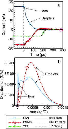
The time-of-flight spectrum can be converted to a mass-to-charge distribution whose integral is the mass flow rate of the beamlet:
[1–3] where x stands for the mass-to-charge ratio, m/q. As illustrated in , we fit the noisy time-of-flight curve to a series of smooth error functions to compute the derivative in the distribution, EquationEquation (2)
[1–3] . shows
for the EAN and EMI-Im beamlets. The sharp peaks near the origin of each curve are the populations of singly charged ions, while the broader bell-like regions correspond to nanodroplets. In the EAN curve, a smaller third peak appears in between, but it is not clear whether this is an artifact of the fitting or it is a second ion population or charged clusters; multiple ion peaks have previously been observed in the time-of-flight waves of electrosprays, corresponding to either the presence of monomers, dimmers, and additional aggregation states in the beams or the emission of a particular ion from different locations in the cone-jet (e.g., from the base of the jet and from the jet's breakup region). Given the areas under the distributions, it is clear that the molecular ion component is a negligible fraction of the molecular flux and, for the purpose of sputtering, both beams can be regarded as solely made of nanodroplets.
We define the average specific charge of the droplets as the ratio between the current associated with the droplet population and the mass flow rate of the beamlet , and use this value to compute their typical velocity
. The values of
for EAN and EMI-Im are 5505 and 2748 C/kg (we have considered the intermediate peak in the EAN spectrum to be droplets). This definition is somewhat arbitrary, and alternatives such as a weighted average using
or the value of x−1 at the peak of the distribution may be significantly different depending on its broadness. For example, the values of
for the EAN and EMI-Im beamlets are 5882 and 3140 C/kg. The average diameter of the droplets is estimated using
and the assumption that the droplets are charged up to 68% of the Rayleigh limit:
[4] ϵ0 stands for the permittivity of the vacuum, while γ and ρ are the surface tension and the density of the liquid. The 68% charging level was determined from measurements of the diameter and charge of similar droplets (Gamero-Castaño Citation2009).
The relevant physical properties of the liquids are listed in . A previous study has shown that the projectile's molecular mass has a strong effect on the sputtering of silicon: liquids with high molecular mass sputter significantly more atoms and produce rougher surfaces than those with lighter molecules (Borrajo-Pelaez and Gamero-Castaño Citation2015). The selection of EAN and EMI-Im for this study was based on these findings. The electrical conductivities in were measured at room temperature, while the density and surface tension are taken from published work. summarizes beamlet parameters. The droplets, with diameters just over 10 nm, are relatively small: this choice is motivated by the need to maximize the impact velocity and, consequently, maximize the specific charge; the specific charge increases with decreasing droplet diameter, see EquationEquation (4)[4] . The electrospraying of these small nanodroplets requires liquids with sufficiently high electrical conductivities, typically above 1 S/m. EAN fulfills this constraint at room temperature, while EMI-Im was electrosprayed at 70°C to produce the desired projectiles. The electrosprays are also operated near their minimum stable current to maximize the specific charge. Although the diameters of these nanodroplets are still between two and three times larger than those of the biggest gas cluster ions used for sputtering (e.g., a very large
gas cluster ion has an estimated diameter of 6.5 nm), the maximum impact velocities in this study greatly exceed those of the clusters due to the much higher charge-to-mass ratio of the electrosprayed nanodrops (Seki et al. Citation2006). lists two values for the impact velocity, molecular kinetic energy, and stagnation pressure, which correspond to the minimum and maximum acceleration voltages used for each liquid; the maximum values of 17.4 km/s, 423 eV per molecule, and 190 GPa are significantly higher than in previous nanodroplet sputtering work.
TABLE 1 Relevant physical properties of EAN and EMI-Im: molecular formula and mass, (amu); estimated molecular diameter,
(nm); density, ρ (kg/m3); surface tension, γ (N/m); electrical conductivity, K (S/m)
TABLE 2 Beamlet parameters: electrospray current, IE (nA); droplet current and mass flow rate, ID (nA) and (kg/s); average charge-to-mass ratio and typical droplet diameter,
(C/kg) and d (nm); number of molecules in the droplet,
; acceleration voltage,
(kV); average droplet velocity,
(km/s); molecular kinetic energy,
(eV); stagnation pressure
(GPa). The pairs of values in the last four columns correspond to the lowest and highest acceleration voltage
In a typical experiment, the beamlet strikes a point in the target for 600 s at fixed target potential. This is repeated at different points and potentials to characterize the sputtering yield as a function of the acceleration voltage. We use a mechanical profilometer to measure the volume of sputtered material, and an atomic force microscope, AFM, to obtain high-resolution maps of the surfaces. The surface roughness is calculated as the root mean square of the AFM maps. We use the following figures of merit to quantify the sputtering data: the sputtering yield Y, or average number of atoms ejected per molecule in the projectile,[5] where
is the density of the target;
is the number of atoms in the unit cell of the crystal, and
is the sum of their masses;
is the volume of substrate sputtered by the beamlet;
is the molecular mass of the nanodroplet;
is the mass flow rate of the beamlet; and
is the time during which the beamlet strikes the target to remove the volume
. The sputtering yield of a 10 nm droplet, Y10, is
[6] where N10 is the number of molecules in a droplet with a diameter of 10 nm. The sputtering rate R, or speed at which the target is carved
[7] where A is the frontal area of the region carved by the beamlet. The kinetic energy of a molecule, Em,
[8]
The kinetic energy of a 10 nm droplet, E10,[9] and the stagnation pressure of the projectile,
.
[10]
3. SIMULATION METHODS
The Molecular Dynamics package LAMMPS is used to model the impact of a 10 nm droplet on [100] silicon (Plimpton Citation1995). The droplet is built as a hexagonal-closed-packaging arrangement of pseudo atoms, each one representing a molecule of the ionic liquid. In the case of the EMI-Im drop, there are 1243 pseudo atoms with masses of 391.31 amu and radii of 0.42 nm (the radius is chosen to match the densities of the projectile and the liquid), while there are 3682 pseudo atoms for EAN with masses and radii of 108.1 amu and 0.29 nm. The silicon target has a thickness of 43.5 nm in the direction of the impact, a 54.3 × 54.3 nm2 frontal area, and is filled with 6,420,000 atoms. The slab is relaxed before the impact for 20 ps with a 293 K Berendsen thermostat applied to all boundaries except for the impact face (Samela et al. Citation2005). The initial velocities of the projectiles are set to 10 km/s for the EMI-Im drop and 11.0 km/s for EAN, to impose equal stagnation pressure of 76 GPa and total kinetic energy of 249 keV. The impact is integrated over 70 ps with a timestep of 0.25 fs, while maintaining the thermostat to eliminate the reflection of shock waves from the boundaries of the computational domain. The forces between the target atoms are calculated with the Stillinger–Weber potential (Stillinger and Weber Citation1985), a widely used and accurate potential for silicon. The forces between the pseudo atoms of the projectiles, and between them and the silicon atoms are calculated with the Ziegler–Biersack–Littmark (1985) potential; in the parameterization of this potential we use the aggregate atomic number of the molecule as the atomic number of the pseudo atom. A more detailed description of the potentials, the thermostat, and other features of the simulations can be found in Saiz and Gamero-Castaño (Citation2014).
4. EXPERIMENTAL RESULTS
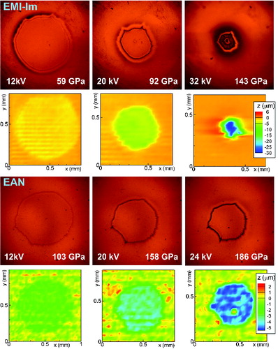
shows pictures and profilometer measurements of the Ge target, bombarded by both EMI-Im and EAN nanodroplets. The pictures are taken with an optical microscope, and have the same magnification for a given liquid. At the lower acceleration voltages, the beamlets carve flat and near circular depressions. The diameter of the depression decreases with increasing acceleration voltage due to the inward bending of the droplets’ trajectories by the planar electric field between the extractor and the target. At the highest acceleration voltages of the EMI-Im beamlets, the shrinking depression becomes distorted due to astigmatism, caused by the increased focusing of the field around the pinhole (in this zone the electric field is not planar, but exhibits a radial component), and imperfections in the axial symmetry of the source. Typical depression diameters for the lowest and highest acceleration potentials are 1 and 0.2 mm for EMI-Im and 1 and 0.6 mm for EAN. The focusing of the beam is obvious in the crater carved by EMI-Im at 32 kV, which, having a diameter of 0.23 mm, is smaller than the pinhole. The depth of the craters increases with acceleration voltage due to both the positive correlation between sputtering yield and projectile velocity, and the shrinking image of the beam. The average depths of the Si, SiC, GaAs, and Ge depressions carved by EMI-Im are 0.5, 0.8, 1.6, and 1.7 μm at VA = 12 kV; and 7.0, 7.0, 18.0, and 15.7 μm at VA = 32 kV. In the case of EAN, these values are 0.4, 0.7, 0.9, and 1.2 μm at VA = 8 kV; and 1.3, 1.7, 3.1, and 2.8 μm at VA = 18 kV.
FIG. 3. Photographs and profilometer measurements of areas sputtered by the EMI-Im and EAN beamlets on a germanium target, at different acceleration potentials.
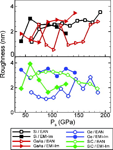
shows the roughness of the bombarded surfaces as a function of stagnation pressure. The values are relatively low and independent of the projectile's stagnation pressure, remaining always under 4 nm for all semiconductors. In addition, the molecular mass of the projectile does not have a noticeable effect on this property either. The present values continuously extend previous measurements at lower stagnation pressures (up to 39 GPa), of the bombardment of these semiconductors by EMI-Im (Borrajo-Pelaez et al. Citation2013). The only anomaly in the topography of these targets is the very strong dependence of the roughness of silicon on stagnation pressure below 30 GPa, for the case of liquids with high molecular mass: in this lower velocity range, the roughness produced by liquids like EMI-Im and TPP is much higher than that produced by liquids with light molecules like EAN and formamide; furthermore the roughness for the high molecular mass liquids displays a strong maximum around 20 GPa, and drops sharply afterward transitioning toward the values measured in the present study (Borrajo-Pelaez et al. Citation2013; Borrajo-Pelaez and Gamero-Castaño Citation2015).
FIG. 4. Roughness of the Si, GaAs, Ge, and SiC surfaces bombarded by EAN and EMI-Im beamlets, as a function of the projectile's stagnation pressure.
shows the sputtering yield as a function of the kinetic energy of the EAN and EMI-Im molecules. Despite the lower specific charge of the EMI-Im drops, their maximum molecular kinetic energy doubles that of EAN due to its larger molecular mass and the higher acceleration voltages possible in negative electrospraying mode. extends the range of impact energy previously studied with EMI-Im nanodroplets (up to 105 eV); the low energy range of the present data matches well the upper energy range of the earlier measurements (Borrajo-Pelaez et al. Citation2013). The sputtering yields for the EAN beamlet increase monotonically with the molecular kinetic energy, reaching maximum values of 1.3, 2.9, 3.3, and 3.9 for Si, GaAs, Ge, and SiC at kinetic energies between 150 and 165 eV. The sputtering yields for the EMI-Im beamlet are several times larger, increasing monotonically for Ge, and flattening at the highest energies for Si, GaAs, and SiC. The maximum sputtering yields occur at molecular energies between 250 and 380 eV, and are 4.3, 9.4, 10.9, and 11.5 for Si, GaAs, Ge, and SiC, respectively. Although the overlap of kinetic energies for both liquids is narrow, the data suggest that EMI-Im sputters all semiconductors more efficiently than EAN. For example, at the highest common energy of 165 eV, the ratio between the sputtering yields of EMI-Im and EAN are 2.2, 2.9, 2.9, and 2.1 for Si, GaAs, Ge, and SiC, respectively. This suggests that other impact parameters besides the molecular energy play an important role in the ejection of atoms. The sputtering yields in are significantly higher than those of gas cluster ions, and comparable to other ion beam techniques using smaller projectiles. For example, a very large gas cluster ion, Ar+10,000, with a diameter of 9 nm similar to our nanodrops, has a sputtering yield of 0.0012 Si atoms per Ar atom, at 20 keV acceleration voltage (Seki et al. Citation2006); the sputtering yield of SiC by an Ar+ ion beam is lower than 2 at the much higher kinetic energy of 15 keV per ion (Pugacheva et al. Citation1997); the sputtering yields of Si and SiC milled by a Ga+ focused ion beam are 2 and 2.5, at kinetic energies between 20 and 30 keV (Steckl and Chyr Citation1999); and reactive etching of silicon by gas cluster ions (∼2000 atoms per projectile) combined with SF6 has a yield of 1.1 (Matsuo et al. Citation1996).
FIG. 5. Sputtering of Si, GaAs, Ge, and SiC by nanodroplets of EAN and EMI-Im, plotted in the form of (a) sputtering yield vs. molecular kinetic energy, and (b) total sputtering by a droplet 10 nm in diameter, as a function of its kinetic energy.
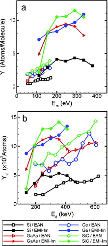
shows the sputtering by a hypothetical 10 nm droplet as a function of its kinetic energy. The extrapolation based on Equations Equation(6)[6] and Equation(9)
[9] is justified by the proximity of the experimental diameters to 10 nm, and allows a direct comparison between EAN and EMI-Im and assessing whether nanodroplet sputtering is a continuum phenomenon: if nanodroplet sputtering were governed by the laws of continuum media, droplets with the same energy and diameter would eject similar numbers of atoms regardless of the nature of the liquid. Although this is a reasonable hypothesis based on the large diameter of the projectiles compared to the size of the molecules, the consistently higher sputtering of the EMI-Im drop observed in proves it to be incorrect. For example, the average ratio between the sputtering by the 10 nm EMI-Im and EAN drops is 1.8 for Si, 2.0 for GaAs, 1.7 for Ge, and 1.5 for SiC. Instead, suggest that the physics of nanodroplet sputtering are driven by collisions between atoms and molecules proceeding in the absence of local thermodynamic equilibrium. This conclusion, previously proposed for the sputtering of silicon (Borrajo-Pelaez and Gamero-Castaño Citation2015), is now shown to be an intrinsic characteristic of nanodroplet sputtering.
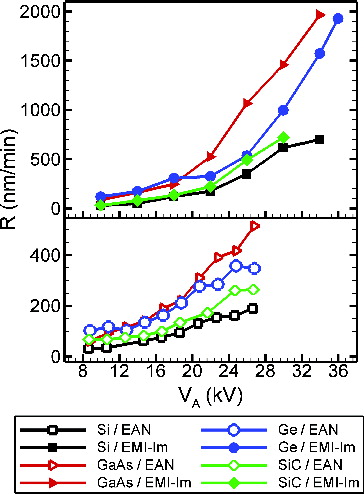
shows the sputtering rate as a function of the acceleration voltage. The sputtering rate is proportional to the sputtering yield and the beamlet's molecular flux, which increases with focusing. As the acceleration voltage increases so does the focusing and the sputtering yield, and consequently the sputtering rate. However, it is apparent that the superlinear dependence of the sputtering rate on acceleration voltage is mostly a focusing effect, because the variation of the sputtering yield with acceleration voltage is modest (). This is also confirmed by the significant reduction of the area of the craters in at increasing acceleration voltage. The maximum sputtering rates for EAN range between 190 and 515 nm/min for Si and GaAs. The maximum rates for the EMI-Im beamlet are 700, 1960, 1930, and 720 nm/min for Si, GaAs, Ge, and SiC, respectively. These high sputtering rates are only comparable to those of reactive ion etching. For instance, sputtering rates for SiC of up to 320 nm/min have been reported with a SF6 plasma (Cho et al. Citation2000), and up to 970 nm/min with an inductive coupled plasma (Khan and Adesida Citation1999). We have not attempted to optimize the sputtering conditions in these experiments, and higher rates for this purely physical sputtering process can be obtained by adjusting beamlet parameters such as the electrospray mass flow rate, the molecular mass, the distance between the emitter and the target, the acceleration voltage, and the shape of the electric field.
FIG. 6. Sputtering rates on Si, GaAs, Ge, and SiC, bombarded by beamlets of EAN and EMI-Im nanodroplets.
5. SIMULATION RESULTS AND DISCUSSION
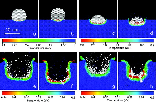
shows snapshots of a central cross-section of the silicon target and the 10 nm projectile, for both EAN and EMI-Im. The impact velocities are 11.0 km/s for EAN and 10 km/s for EMI-Im, which make the stagnation pressure and the kinetic energy of the projectiles identical, 76 GPa and 249 keV. The ratio between the projectile's diameter and its velocity, d/v, is used as time scale. The molecules of the projectile are shown in white, while the color graduation of the target indicates the temperature field. The temperature at a point is computed by the customary average of kinetic energies, in this case of N atoms enclosed in a spherical control volume of radius 1.09 nm centered at the point:
[11]
FIG. 7. Molecular dynamics simulations of the impact of EAN and EMI-Im nanodroplets on silicon. The projectiles are 10 nm in diameter and have an identical kinetic energy of 249 keV (11.0 km/s impact velocity for EAN and 10 km/s for EMI-Im). The snapshots are taken at 0.4, 1, 5, and 8 d/v time units. Panels a, c, e, and f correspond to EAN, while the impact of the EMI-Im drop is captured in panels b, d, f, and h.
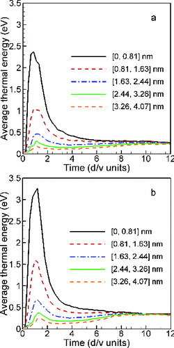
provides more quantitative information about the energetic state of the atoms near the surface; this is the region of interest for sputtering because, due to the low penetration of the projectile's molecules, the ejection of atoms is fully determined by the energetic state and processes occurring in the outermost layers. shows the average thermal energy per atom as a function of time from impact (in d/v units), and distance from the surface. To construct these curves, we divide the impact region into sequential layers surrounding the crater's surface, each one 0.82 nm thick, and compute the average thermal energy of the atoms in each layer; the thermal energy of an atom is defined as , where the temperature is computed with EquationEquation (11)
[11] evaluated at the position of the atom. The average energy of the outermost atoms peaks at 1.2 ps for EMI-Im and at 0.8 ps for EAN. The maximum energy for EMI-Im is significantly higher than for EAN, 3.26 eV compared to 2.37 eV. Since the surface binding energy of silicon is estimated to be 4.67 eV, i.e., the value of the standard enthalpy of formation of Si(g) (Sevast’yanov et al. Citation2010), it is apparent that these outermost atoms are energetic enough for a fraction of them to be ejected, and that the total ejection will be higher for the EMI-Im projectile. Note also that during the initial phase of the impact the average thermal energy decreases rapidly with distance, and that after approximately 3 d/v time units this large thermal gradient becomes significantly reduced. The largest fraction of the sputtered atoms is ejected during the initial phase of the impact (approximately within the first 3 d/v time units), a period characterized by strong collisionality between atoms and molecules and the absence of local thermodynamic equilibrium; following this period a significant number of atoms are thermally evaporated under, or approaching, local thermal equilibrium (Saiz and Gamero-Castaño Citation2014).
FIG. 8. Evolution of the average thermal energy per atom at varying depth from the surface. (a) Impact of the EAN projectile; (b) impact of the EMI-Im projectile.
The underlying reason for the higher sputtering by the EMI-Im projectile is that, at fixed impact velocity, the heavier EMI-Im molecule has a larger kinetic energy (proportional to its mass), which is transferred to the target through collisions. The resulting knock-on atoms are more energetic, and therefore more likely to overcome the surface binding potential and to be ejected. This ejection mechanism is referred to as nonlinear collision cascades sputtering. In addition, the primary and secondary knock-on atoms that are not ejected distribute the transferred energy more unevenly in the case of impacts by heavier molecules (more uneven both in intensity and spatially, the latter due to the larger separation between molecules), which translates into higher dissipation and temperature fields once local thermodynamic equilibrium is reached. The resulting enhanced thermal evaporation also contributes to the sputtering.
Finally, note that these molecular dynamics simulations do not account for the possibility of chemical interaction between the projectiles and the target, and therefore omit a potential chemical enhancement of the sputtering. Although the presence of fluorine in the EMI-Im molecule, its absence in EAN, and the strong reactivity of this element suggest that chemical enhancement could be the reason for the more efficient sputtering of EMI-Im compared to EAN, we expect this effect to be minor based on the following arguments: the sputtering phenomenology of the ionic liquid TPP, which does not contain fluorine but has a high molecular mass, is similar to that of EMI-Im and different to the low molecular mass liquids EAN and formamide (Borrajo-Pelaez and Gamero-Castaño Citation2015); at the impact energies used in this study it is unlikely that a significant number of covalent bonds in the liquid molecule will break, which is required to produce fluorine radicals (Anders et al. Citation2007); and the molecular dynamics simulations, which do not account for chemical effects, do reproduce the experimental sputtering trends.
6. CONCLUSIONS
The sputtering yields of Si, Ge, GaAs, and SiC bombarded by EMI-Im nanodroplets, previously measured at molecular energies and impact velocities up to 105 eV and 7.2 km/s, continue increasing with impact velocity: in this new study we record sputtering yields as high as 4.3, 10.9, 9.4, and 11.5, respectively, at molecular kinetic energies between 250 and 380 eV. The nanodroplets of the EAN ionic liquid, used here for the first time to bombard Ge, GaAs, and SiC, also cause significant sputtering but at lower yields than EMI-Im. Molecular dynamics simulations of nanodroplet impact on silicon, designed to retain the differences in mass and size of the EMI-Im and EAN molecules, also reproduce the higher sputtering yield of EMI-Im. The increased sputtering by EMI-Im with respect to EAN when the projectiles are otherwise macroscopically identical (i.e., they have the same diameters and kinetic energies) is due both to the higher efficiency of the heavier molecule for transferring enough energy to knock-on atoms to overcome the surface binding potential; and to the higher dissipation, temperature fields and ultimately thermal evaporation caused by the impacts of the heavier molecules. The molecular/atomic collisions driving nanodroplet sputtering proceed in the absence of thermal equilibrium, and therefore the phenomenon is ill suited to continuum modeling. We conclude that, despite the very large size of the projectile compared to interatomic distances, nanodroplet sputtering does not follow the laws of continuum media.
The maximum sputtering rates for Si, Ge, GaAs, and SiC are 700, 1930, 1960, and 720 nm/min, respectively, and were obtained with the EMI-Im beamlet. These values are much higher than for any other technique based on physical sputtering, and comparable to reactive ion etching. They are especially attractive for etching applications requiring high aspect ratios, and for inert materials like SiC and GaN able to withstand chemical attack. Finally, at the high impact velocities used in this study the topography of the bombarded samples does not display a significant dependence on either the molecular mass of the projectile, or the energy of the impact. The roughness of all bombarded surfaces remains relatively low, always below 4 nm.
ACKNOWLEDGMENTS
The authors are grateful for the support of the AFOSR Program Manager Dr. Birkan.
Funding
This work was funded by the Air Force Office of Scientific Research, Grant No. FA9550-11-1-0308.
Related Research Data
REFERENCES
- Anders, C., Kirihata, H., Yamaguchi, Y., and Urbassek, H. (2007). Ranges and Fragmentation Behavior of Fullerene Molecules: A Molecular-Dynamics Study of the Dependence on Impact Energy and Target Material. Nucl. Instrum. Meth. Phys. Res. B, 255:247–252.
- Borrajo-Pelaez, R., and Gamero-Castaño, M. (2015). The Effect of the Molecular Mass on the Sputtering by Electrosprayed Nanodroplets. Appl. Surf. Sci., in press.
- Borrajo-Pelaez, R., Grustan-Gutierrez, E., and Gamero-Castano, M. (2013). Sputtering of Si, SiC, InAs, InP, Ge, GaAs, GaSb, and GaN by Electrosprayed Nanodroplets. J. Appl. Phys., 114:184304.
- Cho, H., Leerungnawarat, P., Hays, D. C., Pearton, S. J., Chu, S. N. G., Strong, R. M., Zetterling, C. M., Östling, M., and Ren, F. (2000). Ultradeep, Low-Damage Dry Etching of SiC. Appl. Phys. Lett., 76:739–741.
- Cloupeau, M., and Prunet-Foch, B. (1989). Electrostatic Spraying of Liquids in Cone-Jet Mode. J. Electrostat., 22:135–159.
- Davison, L. (2008). Fundamentals of Shock Wave Propagation in Solids. Springer-Verlag, Berlin.
- Fernandez de la Mora, J. (1996). On the Outcome of the Coulombic Fission of a Charged Isolated Drop. J. Colloid Interf. Sci., 178:209–218.
- Fernández de la Mora, J., and Loscertales, I. G. (1994). The Current Emitted by Highly Conducting Taylor Cones. J. Fluid Mech., 260:155–184.
- Gamero-Castaño, M. (2008). Characterization of the Electrosprays of 1-Ethyl-3-methylimidazolium bis(trifluoromethylsulfonyl) Imide in Vacuum. Phys. Fluids, 20:032103.
- Gamero-Castaño, M. (2009). Retarding Potential and Induction Charge Detectors in Tandem for Measuring the Charge and Mass of Nanodroplets. Rev. Sci. Instrum., 80:053301.
- Gamero-Castaño, M. (2010). Energy Dissipation in Electrosprays and the Geometric Scaling of the Transition Region of Cone-Jets. J. Fluid Mech., 662:493–513.
- Gamero-Castaño, M., and Fernández de la Mora, J. (2000). Direct Measurement of Ion Evaporation Kinetics from Electrified Liquid Surfaces. J. Chem. Phys., 113:815–832.
- Gamero-Castaño, M., and Hruby, V. (2001). Electrospray as a Source of Nanoparticles for Efficient Colloid Thrusters. J. Propul. Power, 17:977–987.
- Gamero-Castaño, M., and Mahadevan, M. (2009a). Sputtering Yields of Si, SiC, and B4C Under Nanodroplet Bombardment at Normal Incidence. J. Appl. Phys., 106:054305.
- Gamero-Castaño, M., and Mahadevan, M. (2009b). Sputtering Yields of Si, SiC, and B4C Under Nanodroplet Bombardment at Normal Incidence. J. Appl. Phys., 106:054305.
- Gamero-Castaño, M., Torrents, A., Borrajo-Pelaez, R., and Zheng, J. G. (2014). Amorphization of Hard Crystalline Materials by Electrosprayed Nanodroplet Impact. J. Appl. Phys., 116:174309.
- Garoz, D., Bueno, C., Larriba, C., Castro, S., Romero-Sanz, I., Fernández de la Mora, et al. (2007). Taylor Cones of Ionic Liquids from Capillary Tubes as Sources of Pure Ions: The Role of Surface Tension and Electrical Conductivity. J. Appl. Phys., 102:064913.
- Khan, F. A., and Adesida, I. (1999). High Rate Etching of SiC Using Inductively Coupled Plasma Reactive Ion Etching in SF6-based Gas Mixtures. Appl. Phys. Lett., 75:2268–2270.
- Mahoney, J. F. (1998). Microcluster-Surface Interactions: A New Method for Surface Cleaning. Int. J. Mass Spectrom., 174:253–265.
- Mahoney, J. F., Perel, J., Ruatta, S. A., Martino, P. A., Husain, S., and Lee, T. D. (1991). Massive Cluster Impact Mass-Spectrometry—A New Desorption Method for the Analysis of Large Biomolecules. Rapid Commun. Mass Spectrom., 5:441–445.
- Matsuo, J., Toyoda, N., and Yamada, I. (1996). Nanofabrication Technology by Gas Cluster Ion Beams. J. Vacuum Sci. Tech. B, 14:3951–3954.
- Plimpton, S. J. (1995). Fast Parallel Algorithms for Short-Range Molecular-Dynamics. J. Comput. Phys., 117:1–9.
- Pugacheva, T. S., Jurabekova, F. G., Miyagawa, Y., and Valiev, S. K. (1997). Computer Simulation of SiC and B4C Sputtering by Ar+ and He+ Ions Bombardment. Nucl. Instrum. Methods Phys. Res. B, 127:260–264.
- Saiz, F., and Gamero-Castaño, M. (2014). Atomistic Modeling of the Sputtering of Silicon by Electrosprayed Nanodroplets. J. Appl. Phys., 116:054303.
- Samela, J., Kotakoski, J., Nordlund, K., and Keinonen, J. (2005). A Quantitative and Comparative Study of Sputtering Yields in Au. Nucl. Instrum. Meth. B, 239:331–346.
- Seki, T., Murase, T., and Matsuo, J. (2006). Cluster Size Dependence of Sputtering Yield by Cluster Ion Beam Irradiation. Nucl. Instrum. Meth. Phys. Res. B, 242:179–181.
- Sevast’yanov, V. G., Nosatenkob, P. Y., Gorskiib, V. V., Ezhovc, Y. S., Sevast’yanova, D. V., Simonenkoa, E. P., and Kuznetsova, N. T. (2010). Experimental and Theoretical Determination of the Saturation Vapor Pressure of Silicon in a Wide Range of Temperatures. Russ. J. Inorg. Chem., 55:2073–2088.
- Sigmund, P. (1969). Theory of Sputtering. I. Sputtering Yield of Amorphous and Polycrystalline Targets. Phys. Rev., 184:383–416.
- Steckl, A. J., and Chyr, I. (1999). Focused Ion Beam Micromilling of GaN and Related Substrate Materials (sapphire, SiC, and Si). J. Vac. Sci. Technol. B, 17:362–365.
- Stillinger, F. H., and Weber, T. A. (1985). Computer-Simulation of Local Order in Condensed Phases of Silicon. Phys. Rev. B, 31:5262–5271.
- Sugiura, J., Lu, W. J., Cadien, K. C., and Steckl, A. J. (1986). Reactive Ion Etching of SiC Thin Films Using Fluorinated Gases. J. Vac. Sci. Technol. B, 4:349–354.
- Walsh, J. M., Stradling, G. L., Idzorek, G. C., Shafer, B. P., and Curling, H. L. (1993). Microparticle Impacts at Ultra-High Velocities: Their Relation to Macroparticle Impacts. Int. J. Impact Eng., 14:775–784.
- Yamada, I. (2014). Historical Milestones and Future Prospects of Cluster Ion Beam Technology. Appl. Surf. Sci., 310:77–88.
- Ziegler, J. F., Biersack, J. P., and Littmark, U. (1985). The Stopping and Range of Ions in Solids, Vol. 1, Pergamon Press, New York.