
 ?Mathematical formulae have been encoded as MathML and are displayed in this HTML version using MathJax in order to improve their display. Uncheck the box to turn MathJax off. This feature requires Javascript. Click on a formula to zoom.
Abstract
Electric spike emission was observed for the first time for thin polymer foils irradiated with low energy light ion microbeams at overlapping fluences, when placing them in between two vessels filled with etchant and distilled water, respectively, and applying a low sinusoidal transverse voltage. The various shapes of recorded spike types are described and examined. From their emergence that occurs after different derived etching times, and the inter-correlation of different spike parameters, we draw the first conclusions about their formation mechanism, behavior, and usefulness for technical applications.
1. Introduction
Extensive information has already been obtained in the area of electric spike (discharge) emission from individual etched swift heavy ion (SHI) tracks in (essentially) polymers, when putting the foils in between two liquid-filled vessels and applying some (usually alternating) potential difference of a few volts across them. Meanwhile, during our new work on the etching of polymer foils, which were irradiated by overlapping slow light ions (SLI) within µm-sized microbeams (yet unpublished), we have also recorded the first electric spikes. This indicates that spike emission is a more general feature of all etched ion-irradiated polymers (which are exposed to a transverse electric field of up to some kV/cm during etching), and that it is neither restricted to the precondition of high energy heavy ion irradiation, nor to the question whether one deals with single or overlapping ion impact. Therefore, we compile in this work the first findings on different types of electric spikes found after the etching of polymer foils which had been irradiated by SLI-microbeams at higher fluences and probing the etching progress via applying an alternating voltage between both foil sides. Thereafter we work to understand the possible mechanism of spike emission from these samples. However, in order to set the base for this discussion, let us first summarize the present knowledge on spike emission from etched ion-irradiated polymers, which was hitherto been restricted to spikes originating from the etched SHI-irradiated polymers only. Also, let us note that so far, nearly all polymer samples examined for spike emission (including those for the present paper) are essentially restricted to the polyethylene terephthalate (PET) foils; at least this polymer shows reasonable wetting when exposed to an alkaline etchant, as its surface acquires negatively charged carboxylate groups rigidly bound to the surface. Accordingly, the local concentration of negative ions (co-ions) decreases on the surface, which favors wetting and penetration of liquids.
2. The present database: Current spike emission and synchronization of individual SHI-irradiated tracks
2.1. Spike emission
2.1.1. Polymeric radiation chemistry
Polymers are solids that contain some intrinsic free volume (FV), resulting from some spatial misalignment of the randomly distributed polymeric chains. In a polymer lattice at elevated temperatures, these FV elements are not fixed but continuously change their shapes and positions due to the polymer chains’ Brownian motion. If a polymer is irradiated by SHI, additional narrow, long, and straight trails of high radiation damage – including some additional FV – will be introduced into this material (Citation1). The overall (intrinsic and radiative) FV facilitates the penetration of water and other impurities into and across polymer foils, essentially along the SHI-introduced ion tracks. I.e. the ion tracks within a thin polymer foil may act as both “irrigation channels” (to deliver water rapidly from the outside into the entire interior of the polymeric foil, thus leading to water uptake and swelling), and – in the case of conductive impurities such as salt water – as “liquid wires” connecting electrically one foil side to the other, with the penetration mechanism being a combination of diffusional (in the undestroyed matrix areas) and capillary-driven motions (i.e. along the pristine and radiation-induced FV zones). However, if we consider that chemically reactive radiochemical products are also formed in the ion tracks, the transport of impurities along these tracks may eventually be somewhat hindered by these obstacles. In any event, the general findings show that, the higher the polymer’s radiation damage is, the faster water penetration across the tracks will be, and consequently also the track conductivity (Citation2).
2.1.2. Penetration through ion tracks
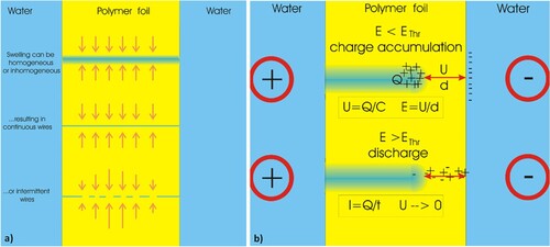
In a typical example with ∼ 10 µm thick PET foils embedded in water, which were previously irradiated by some 109 SHI/cm2, the overall foil resistance was found to be in the order of some 10–20 MΩ, by applying a low frequency alternating voltage across the foils and recording the transmitted signals with an oscilloscope (Citation3). This means the typical resistance of an individual latent SHI track is in the order of ∼ 5 × 10¹⁶ Ω. However, subsequent swelling (i.e. expansion due to water uptake) of the surrounding polymer matrix into the empty track zone increases the track resistance due to the decreasing diameter of the “liquid wire” across the polymer foil (i.e. some of the adsorbed water is “squeezed out” from the track again), until some new equilibrium value is established along the whole track length. This may either enable a lower, but smooth current flow permanently across the track, Figure (a) (center). It may, however, also happen that the “liquid wire” along a track becomes partially or completely blocked so that transient currents are interrupted, Figure (a) (bottom). Upon application of some voltage with suitable height across the polymer foil, in such a case current breakthrough across the closed track segments may occur. This is explained as shown in Figure (b): when, after applying an external voltage U across the foil, the electric field strength E across the remaining insulating polymer layer with thickness d is still below some critical threshold field strength EThr, charges Q will accumulate in the liquid wire until EThr is exceeded. Then, a spark-like current I = Q/t flows transiently across the barrier for a short time t until the discharge ends and the system returns to the previous stage. Such spike emission from either latent or etched ion tracks in polymers embedded in electrolytes (Citation4, Citation5) has previously been observed.Footnote1 They are accompanied by a transient negative differential resistance (Citation1, Citation10), so that such structures are useful as active electronic building blocks.
Figure 1. (a) The effects of polymer swelling by water uptake on the nature of the “water wire” within a latent track; (b) explanation of the charge accumulation with subsequent discharge along an obstacle within a water-filled track (Citation3, Citation5, Citation10). The thickness d of the remaining foil segment separating the etched track from the opposite surface is given by d = U/E, with E being the breakthrough field strength – for PET it is 19–160 V/µm.
2.1.3. Different spike types
Depending on the experimental conditions, we had observed two different types of current spikes, those emitted randomly in time, and those emitted (more or less) regularly. In order to get some more insight about the nature of these different types, both were analyzed by Fourier-transform spectroscopy, as a function of time (Citation3, Citation9).
The random spike emission with transient short uncorrelated spikes of fluctuating intensity is usually followed by a sudden voltage drop (due to the emergence of some negative differential resistances, NDR). This is not only common for charge transmission across individual etched SHI tracks (as prepared by A. Schulz et al. (Citation11) and recorded by Z. Siwy et al. (Citation12)), but also across all other multiple track-based devices (Citation5, Citation10, Citation13). Sometimes, however, randomly emitted spikes start synchronizing by interacting with each other, thus gradually establishing more clear-cut permanently stable (“phase-locked”) emission features. Our Fourier analysis of these spikes (Citation3, Citation9) revealed spectra with a central emitted frequency and several more or less equidistant higher ones; it took some ∼ 3 min before perfect synchronization was achieved.
All experimental results on synchronized spike emission can be well described (Citation7, Citation14–19) by either a potential well model approach (Citation14, Citation15), or by Molecular Dynamics (Citation16), as concerns, e.g. the critical frequency and critical voltage to be overcome for spike emission, the number of the optima in the spike’s current/voltage emission patterns, and the optimum spike emission frequency. The latter reflects favored occupancy numbers of charge carriers per track, which yields the highest spike pattern stability. The patterns show up most pronounced at rather equidistant applied voltages.
2.2. Collective current spike effects in SHI tracks: spike synchronization
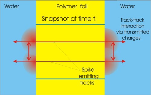
In the case of spike emission from closely neighbored SHI tracks (with SHI fluences exceeding ∼ 108 cm−2), local charge clouds emitted from each of them behind the polymer foil within an adequate time interval, interact with each other and synchronize; Figure (Citation17, Citation19, Citation20). Thus, the recorded pulses become much more pronounced and gradually arranged within well-defined frequencies. Synchronization stemming from lateral track-track crosstalk (via some mean migration pathlength λ of the charge carriers along the sample surface, perpendicular to the track direction) becomes better the closer the tracks are, i.e. the higher the particle beam fluence is. However, when track overlapping sets on (∼ 4 × 109 cm−2), synchronization gradually vanishes due to the simultaneous onset of polymer carbonization.
Figure 2. Illustration of the cross-talk of two neighbored spike-emitting SHI ion tracks (Citation3, Citation9). For ∼ 150 nm < λ < ∼2–3 mm, full lateral track-track cross-talk is possible, with λ being the average track-track distance. Optimum cross-talk is obtained for λ being slightly above the minimum distance of 150 nm. For λ < 150 nm, polymer carbonization sets in, resulting in the sample’s destruction. For λ > 2–3 mm, when the time required for full charge synchronization is exceeded, synchronization worsens dramatically (these numbers hold for typically applied potentials U = 1 … 5 V and frequencies around ∼ 1 Hz in the corresponding experiments).
As complete track-track interaction with each other after charge transmission is possible only within λ (which depends on the available migration time = half period of the applied frequency), one may define some “region of interest” of synchronization ROIsync = λ2 around each track as the size where near-perfect synchronization is found. As is the case for the emission of individual spikes from liquid-filled etched SHI tracks, also the emission of synchronized spikes is influenced by a number of specific parameters, such as the fluence of the track-forming impinging energetic ions, and the spike emitting sample size.
For high fluences and rather small irradiated sample areas (∼ 10 mm2, corresponding to λ ∼ 2–3 mm; denoted by us as “domains”), stable synchronous spike emissions were found in test measurements at least for several days (Citation21), thus reconfirming the mechanism of “phase locked synchronization” (Citation22). However, for sample sizes exceeding fully synchronized domains (tested up to 1 cm2), increasing fluctuations in the spike patterns with time emerge (Citation14) that obscure clear synchronous spike emission. Nevertheless, even in such cases with incomplete spikes’ information exchange, it is remarkable that some residual synchronization still takes place, which one might understand as some kind of “synchronization of synchronized domains”.
2.3. Spike emission from etched PET irradiated by SLI?
The energy transferred by individual SLI ions, as compared with SHI ions, is so small that any track formation is rendered impossible. As the deposited energy density in a target spot by one SHI impact is around 2 orders of magnitude larger than that of one SLI, any possible spike emission from etched SLI-irradiated polymers is expected to make sense only for polymers that have been irradiated by SLIs multiple times.
Any energetic ion impact onto a polymer region is known to lead to the material’s destruction via chain scissioning (CS) (Citation23–26), hence to the formation of smaller radiochemical products, the smallest of them being volatile (so that they escape in vacuum or gas) or soluble (so that they can escape in liquids such as the etchant liquid). As a result, the polymer’s overall FV increases. For a spike to emerge, the ion fluence must exceed some minimum value to produce a sufficiently high FV. Only then sufficient charge carriers can be accumulated within the polymer foil’s FV, to be ejected in a pulse. Further, some mechanism must exist to enable the ion’s transient passage, after which it should close again. To our present understanding, there exist three possibilities to accomplish this:
One can exploit some mechanical material’s property, such as elasticity to open or close the access to the FV upon requirement.
Some mobile charge clouds could enable or prevent the ion’s transmission across the radio-porous polymer (e.g. by charges transiently bonding to the FV boundaries).
One could attach some pristine polymer layer onto the ion-irradiated zone. This can be accomplished by simply using a polymer foil with a thickness slightly exceeding the range of the implanted ions, so that some pristine polymer remains beyond the irradiated zone. After multiple irradiation, when the density of the irradiated region increases, the adjacent pristine zone is put under high strain. Polymers under strain, however, easily exhibit craze and crack formation, so that some conducting connection towards the foil surface can easily be established after etching. The pristine polymer’s elasticity will then control the transient charge passage.
There should exist an upper limit for the ion fluence, as with increasing CS, when more and more radiochemically reactive products emerge, random recombination processes (cross-linking, CL (Citation27–30)) also grow in the irradiated zone, which make the structure more rigid, till excessive rigidity will finally prevent any elasticity. Also, target carbonization, as an extreme consequence of SLI overlapping, must, of course, be avoided, as it leads to pore closure, zero elasticity, and increasing foil conductivity (Citation31–34), which prevents spike emission. Therefore, we consider the region above ∼ 1011 cm−2 (i.e. around 1000 SLI impacts on spots of ∼ 1 µm), within an order of magnitude, as the most reasonable fluence range for producing spike-emitting polymer foils.
Another remark in this connection: SHI impact onto polymers introduces a tremendous shock wave around each ion that reduces the FV in the SHI track neighborhood dramatically. As, for comparison, this property is nearly completely missing for SLI, one should expect that target compaction hardly plays any role after SLI impact, even upon considerable ion impact overlapping. This means the sample’s FV – a precondition for enabling ionic current transmission across the samples – should remain rather unaffected by the SLI irradiation. Consequently, only relatively little subsequent etching (as compared with SHI-irradiated polymers) should be required to open the FV so much that current transmission can be recorded.
As compared with SHI irradiated polymers with their straight and long ion tracks as more or less empty zones after some etching, possible spikes emerging from overlapping SLI irradiation after etching must overcome more obstacles, such as given by randomly winding pore paths with varying diameters, and the presence of larger radiochemical products along them (in SHI tracks, the average size of the radiochemical destruction products will be smaller as higher energy density is available for their decomposition; and due to their smaller sizes, they can escape easier). This means we expect that SLI-based spikes should be smaller (due to higher Ohmic pore resistances to overcome) and slower (due to longer and more difficult charge migration paths) as compared with SHI-induced spikes – but nevertheless, they are expected to exist!
3. Experimental
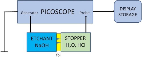
3.1. Transmitted Current Spectroscopy (TCS) as an analytical tool for controlled etching
For several decades, our main tool for the examination of radiation-damaged polymers is the Transmitted Current Spectroscopy (TCS, Figure ) – as an example, see e.g. (Citation1, Citation10). TCS is useful for detailed studies on the pore opening during etching, and for the emergence of the etched track tips in their early stages, i.e. for relatively small pore diameters. By application of sinusoidally alternating voltage, one can, in principle, also derive additional information about capacitive/inductive/memristive effects from the I/V phase shifts, and eventual rectification of the transmitted currents points at charge carrier bonding to the walls of the intrinsic nanoporous system. Further, variation of the applied frequency yields information about the molecular vibration states of the materials embedded in the irradiated polymer matrix. Fourier spectroscopy allows one to determine the dynamics of the system’s frequency spectrum during etching, and Bode plots allow one to study further the frequency response of the system to external influences in even greater detail.
Figure 3. Principle sketch of TCS: a voltage generator (above) feeds sinusoidal signals into the etchant half-vessel (below, left; usually NaOH is used as the etchant). The signal passes the central foil from its cis-side towards its trans-side on the way to the stopper half-vessel on the opposite right (trans) side (usually containing H2O or HCl, to neutralize the etchant more rapidly) The transmitted signals are collected by the “probe” section where the signals are processed and fed into the display and storage unit.
3.1.1. Instrumental limitation: full etchant breakthrough
Though the used technique TCS is excellent for detecting and characterizing the tiniest open pores in ion-irradiated and etched polymers, it has instrumental limitations if very large etched track diameters have to be examined. This limit is reached when the transmitted electric currents across the foil have obtained their maximum possible values; the corresponding etching time is defined as t100%.
For illustration, see the principle measuring circuit in that TCS case, Figure : A voltage generator operating at a voltage U is connected with the sample etching vessel (filled with etchant and/or another electrolyte) via an electrode inserted into one of the two compartments of this vessel. In the case of an open pore separating both compartments from each other, an electrical current I is allowed to flow across the pore towards a probing electrode in the opposite compartment, which is also filled by an electrolyte. This signal recorded by the probe in that opposite compartment is sent via a shunt with resistance Rshunt (1 MΩ in our experiments) to the measuring oscilloscope with an output impedance Rint (600 Ω for Picoscope). Hence the current recorded by the oscilloscope is I = U/R with R = Rfoil + Rshunt + Rvessel + Rint, R being the overall resistance of the measuring circle, and Rfoil being the resistance of the irradiated foil.
For the case of SHI-irradiated polymers with straight ion tracks emerging, etched track radii could be easily obtained from the value of Rfoil derived via the above correlation. In such cases, typical average track radii in the order of ∼20 … 30 nm are found at the onset of etchant breakthrough, when non-zero currents start flowing. However, for etched overlapping SLI irradiated foils, virtually nothing is yet known about the nanopore distributions, geometry or shapes, or average diameters. All details are still speculative, based only on general experience with SHI tracks and TRIM simulations of the spatial energy transfer distributions. Even worse, if the transmitted currents are completely absent (as given e.g. for sample CON21; when the transmitted currents are virtually zero in between the emitted spikes, see chapter 4.2), it is impossible to obtain any additional information.
For full breakthrough after etching at the time t100%, when the foil resistance Rfoil becomes negligible as compared with the remaining resistances: Rtrack << Rshunt + Rvessel+ Rint, pore values can no longer be determined with sufficient reliability so that any result as calculated from equation I = U/R becomes meaningless. Once TCS experiments have reached this border, the measurement can be stopped.
3.2. Motivation for the chosen experimental procedure
3.2.1. Principle outline
Macrofol (polyethylene terephthalate, PET) foil samples were irradiated by a perpendicularly impinging 13 MeV O5+ ion microbeam of ∼ 1 µm diameter with fluences Φ between 1 × 10⁹ and 1.2 × 1012 cm−2, resulting in irradiated spot sizes of 1 µm2 diameter on the samples, that had suffered the impact of 10 to 12000 SLIs. The degree of this damage was probed by subsequent etching of the irradiated samples. Faster etching speeds than those that are regular (for unirradiated samples) are considered to be an indication of the polymer’s radiation damage by the formation of excess free volume due to degassing; slower etching speeds than usual are essentially ascribed to the polymer’s compaction (i.e. loss of free volume stemming from radiative carbonization). Whenever electric spike emission was observed during the etching process, special attention was given to this sample, and the corresponding results were compiled in this work.
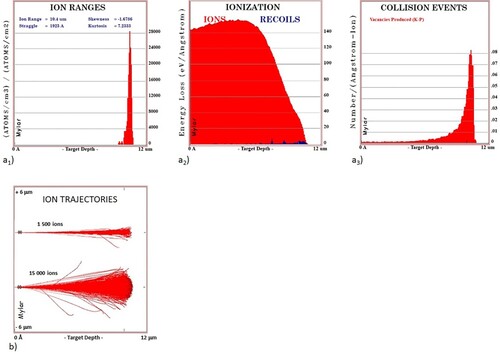
The above ion type was selected as it was the one with the longest range available at the NPI microbeam irradiation facility, with the ion range R in PET being as long as 10.6 m, according to the TRIM prediction (Citation35), Figure . In order to fully incorporate the whole damage (electronic and nuclear) distribution completely within the foil, we used slightly thicker foils of 12
m thickness as targets. This choice had the advantage described in chapter 2.3 that a residual 1.4
m thick pristine polymer layer beyond the irradiated zone could serve as a convenient “valve” for the ion’s retention and transmission, depending on their transient charge accumulation within the nanoporous etched irradiation region. Of course, some slight disadvantage is that, in this case, the breakthrough time is somewhat delayed due to the additional establishment of some conducting connection from the foil’s cis-side (irradiated side) towards the opposite foil trans-side (back side), across the pristine polymer layer beyond the ion’s range.
Figure 4. (a) TRIM simulation of the ion distribution (a1), the electronic energy transfer distribution (a2), and the nuclear energy transfer distribution (a3) of 13 MeV O5+ ions impinging into a 12 µm thick PET foil; (b) TRIM simulations of ion trajectories of these ions in lateral view, for 1500 and 15000 ions per spot (for clarity, both simulations are shown in the same figure). Considering that in the experiments a ∼ 1 µm thick microbeam was used, a more realistic graph for the high-fluence example would indicate a damaged area near the trans-side region with a width of about ∼ 3 µm.
For this work, we used slightly aged polyethylene terephthalate PET foils (here: macrofol of ∼ 2015–2020 provenience). When comparing the bulk etching behavior of freshly obtained PET foils with ours, some aging degradation was obvious from the measured values that had decreased. But for the topic of this work, this does not matter at all, as we always only compared foils of the same batch. Only if one wants to compare the presented results with results from other authors, some adjustment of the time scales will be required.
To avoid possible confusion by eventually inhomogeneous polymer foil compositions on both foil sides, 13 MeV O5+ microbeam irradiation of the 12 µm thick PET foils was always performed on the same foil side (defined as the cis-side) with a well-defined number of ions (between 10 and 12.000), that was impinging randomly on always the same side of the sample within the 1 µm2 beam spot, corresponding to fluences Φ between 1 × 10⁹ and 1.2 × 1012 cm−2. This signifies that we cover the fluence range from the beginning of ion impact overlapping till that one shortly before polymer carbonization.
All samples received a number for unambiguous identification. This number is always on the side of irradiation. To distinguish the sample’s front (cis) and back (trans) sides, the number is written in the upper left corner of the sample, followed by a dot; for example, for sample # CON21: “21”. For all samples, a geometrical reference point was defined by putting 4 small black spots around the central spot on the sample center. This spot helps find the structures in the microscope. This central dot is always drawn on the back (trans side) to avoid its dissolution during etching. Etching with 6 M NaOH at 50 °C from one direction (cis) only is always performed on the same side; the opposite (trans) foil side is submerged into distilled water as an etching stopper after the etchant breakthrough. An alternating sinusoidal voltage of ± 2.0 V with typically ∼80 to 300 mHz frequency was applied across the foils via Ag/AgO2 electrodes; the measuring probe was equipped with a 1 MΩ shunt resistance. Recording of the transmitted current took place with a “Picoscope” oscilloscope as a function of etching time.
Both, the moment when the first etchant ions were capable of transmitting the foil (“breakthrough time”, tB) (thus initiating a non-zero current across the foils), as well as the time t100% when full (100%) transmission across the foil was reached, were recorded. Additionally, the onset and offset times of the current spike emission were noted.
4. Results and discussion
4.1. General Findings
When considering all our hitherto prepared and examined SLI-irradiated samples, spike emission appears to be a rather rare event, amounting to only ∼ 5%. However, considering that spike formation requires certain minimum and maximum ion fluences under which they best form (presently estimated to be around 1 × 1011 cm−2, corresponding to ∼ 1000 ions per microbeam spot of 1 µm2, within ± 1 order of magnitude) and considering only these samples, then the probability of finding spike emissions already doubles. Nevertheless, this signifies that we are still far away from intentionally tailoring specific spike-emitting foils for practical applications; more work must be invested to find out the appropriate strategies to accomplish this goal. As this is the very first work ever dealing with this phenomenon, our database (∼ 100 samples) is still somewhat small. Here, we select only the 4 most interesting samples (according to our nomenclature: CON1, CON21, CON23 and CON33) to describe all the different spike effects in more detail. At present, we cannot yet, e.g. properly explain – apart from “handwaving” arguments – why, e.g. some samples yield small spikes, and others yield high ones. Of course, pulse synchronization is the determining factor in the latter case, but it is not yet clear why synchronization is triggered well in one case and not at all in other cases. Nevertheless, by comparing the etching times during which spike emission started, and the corresponding etchant breakthrough times, we can conclude that they are usually rather close to each other. This signifies that the migration paths across the assumed nanoporous network within the radiation-damaged region after etching are still very narrow, i.e. possibly in the order of ∼20–30 nm or even below (as this is the typical order of magnitude which SHI-based etching experiments indicate during the onset of etchant breakthrough).
Table 1. Overview of the typical properties of representative SLI-irradiated etched samples that showed spike emission.
Amazingly, we found quite a range of different types of spikes, often emerging from the same sample, one after the other, depending on the stage of etching (). It is also remarkable that both spikes and Ohmic currents can either co-exist without interfering with each other (example: sample CON1), or that spikes just emerge as distortions of existing Ohmic currents (samples CON23 and CON33). Still, in another case (CON21), spike ejection was already found though Ohmic currents could not yet be detected (within our measuring accuracy). Possibly, in such samples, some current type dominates in one sample domain, whereas other current types dominate in different domains; thus, the overall appearance is some kind of coexistence of different current types. Observations show that there exist apparently non-synchronized single small spikes with random height and random distance from each other; they can be unipolar or bipolar, starting with either positive or negative voltage. Their lack of correlation indicates that they are not synchronized with any other spike (e.g. sample: CON1). On the other hand, there also exist large narrow spikes with mostly the same heights and narrow widths at a regular distance from each other (sample CON21), clearly pointing at pronounced, possibly even phase-locked synchronization. Similar synchronization also shows up in spike sequences with gradually increasing height. After exceeding some height maximum, the spike sequence either collapses completely, or just drops to some lower value only, from which another increasing group of spikes emerges again. Some 3 to 4 such different consecutive spike groups have been observed (CON1). Sometimes spikes completely vanish abruptly at a certain time, but after some random time spikes may emerge again (CON1). Many such different spike patterns can occur sequentially after each other (CON1, CON23, CON33).
4.2. Pristine sample as reference: CON82
After quite a long period of electronic inactivity, pristine foil samples show sudden etchant breakthrough, signifying that at that moment, the formation of the first continuous conducting pathways between the front and back foil sides was completed after attacking and dissolving the weakest regions of the polymer nanostructure (i.e. etching does not proceed homogeneously across all the foil). The speed of the etchant progress along this first pathway across the sample CON82 was calculated to be ∼ 0.44 nm/s. As spike emission was never found for pristine foil etching, we conclude that spike formation does not depend on the polymer structure itself but that, instead, additional radiation-induced defects are necessary requirements for any spike production after etching of these defects. Some slight rectification of the transmitted current stems from the asymmetric etching from one side only. Further etching leads to the step-wise increasing currents whenever more conducting connections become available.
4.3. Sample CON1
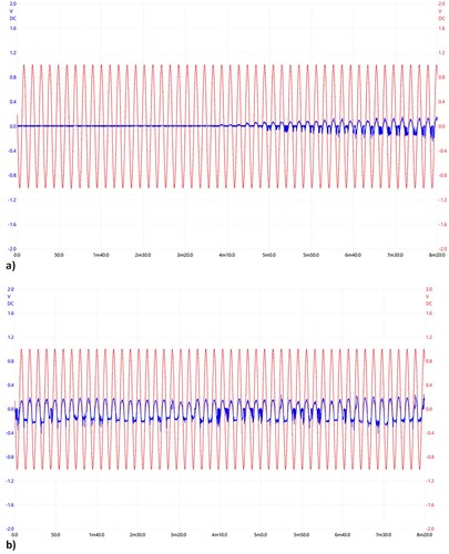
Figure presents two representative original protocols during foil etching. From the sinusoidal transmission signals (blue), one can conclude that, in this case, spike emission started after etchant breakthrough (not shown here). This sample is characterized by many spike sequences of small height, some of which are rising, others falling in height, and some of which first increase and then decrease. Only after prolonged etching times this appearance is occasionally interrupted by phases of single spike emission. Spike sequences appear already shortly after the onset of etching, and they vanish rather abruptly after ∼ 70 min, with a final, quite pronounced double spike.
Figure 5. Etching protocol of sample CON1, irradiated by 1.2 × 10¹¹ ions/cm−2 (i.e. 3 × 1010 cm−2 ions on 4 neighboring spots of ∼ 1 µm2 each); measurement with ± 1 V AC at 261.2 mHz, applied across the sample in the etching vessel. Display (a) shows a detail of the first protocol, which was taken 9 min after the onset of etching, after which some faint breakthrough current showed up nearly immediately; display (b) starts at 39 min after the beginning of etching. All spectra show numerous different tiny pulses overlaying the basic sinusoidal transmission signal. Spike emission stops abruptly after ∼ 70 min, leaving pure Ohmic transmission currents only. Red sinusoidal curves: applied voltage, blue curves: response of current transmitted across the etched foil.
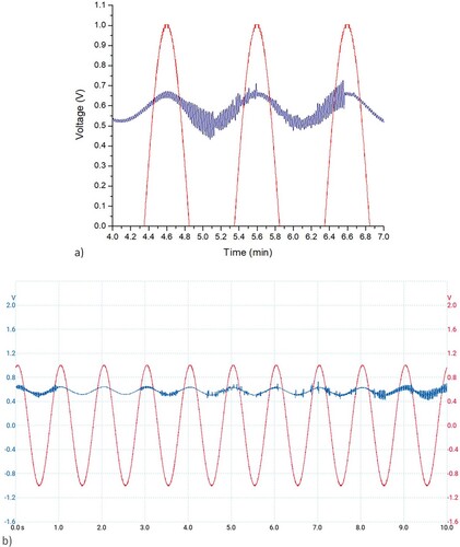
The most pronounced feature of this sample is that, in general, current spikes mostly do not appear as individual entities (as in nearly all other recorded examples), but show up as compact sequences of up to some ∼ 200 spikes or so. Whereas the externally applied voltage operates in this example with 261.3 mHz, all individual spikes – both as individual entities or embedded in sequences – operate with ∼ 20 to 25 Hz, i.e. are roughly 100 times faster. The heights of individual spikes and of spikes within a sequence are comparable with each other – typically in the order of some 20–100 mV.
The evaluation of the observations of this sample is compiled in the graphs of Figure . In Figure (a), the sequential appearance of different types of spike sequences is illustrated schematically as a function of time. There exist: “sequence up” (# 10 in the graph), “sequence down” (# – 10), “sequence up and down” (# 0), “truncated sequence up” (# 5), and “truncated sequence down” spike sequence type (#-5). The “sequence up” spike sequence is characterized by spikes first gently rising from zero to maximum height, and then vanishing abruptly (in this case, often, another “sequence up” group follows. Similarly, the “sequence down” sequences are characterized by spikes suddenly starting with some maximum height, and thereafter gradually decreasing to near-zero). The “sequence up and down” type describes combinations of “sequence up”and “sequence down” groups. This means the spike sequence first gently rises from zero, passes some maximum height, and decreases again towards near-zero. The truncated spike sequences start increasing or decreasing abruptly from some non-zero spike height, and after some time vanish abruptly again. The “sequence up” cases are most abundant, followed by the “sequence up and down” cases; truncated cases occur seldomly, and also the “sequence down” case was observed only once.
Figure 6. Spike emission properties of sample CON1; (a) the type of spike sequence, in dependence of the etching time, (b) correlation of spike sequence maximum heights with etching time. Added are also the time intervals during which no spike sequences show up, but only occasionally individual single spikes. (c) Correlation of spike sequence widths with etching time. d) Correlation of maximum spike heights and widths. Some faint proportionality might eventually show up, but possibly also different correlations hold.
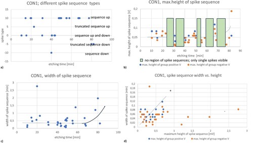
In the subsequent graphs, the maximum heights (Figure (b)) and widths (Figure (c)) of the sequences are plotted as a function of the etching time, and vs. each other (Figure (d)). From Figure (b), it follows that negative spike sequences appear to be more abundant than positive ones, which may stem from the sample’s slight rectification properties. The heights of both positive and negative spikes roughly scatter by the same amount, and their average values are rather constant with increasing etching time, except for the highest etching time > 50 min (corresponding to ∼35 spike sequences), when their height increases. This points to increasing sizes of the internal nanoporous network so that higher charges can be stored, to promote higher spike current sequences for a longer time. However, once the pore diameters exceed some limit, spike emission vanishes. The same tendency as for the heights is also found for the sequence widths, however, with no preferences for negative polarity (Figure (c)); consequently a height/width plot (Figure (d)) may indicate some faint height-to-width proportionality. There is, however, also some indication that both positive and negative heights follow independently different correlations, with negative spike sequences deviating strongly from proportionality. Due to the currently still large dispersion of the data, we have to leave the final interpretation still open. Figure (b) also illustrates another interesting collective behavior, insofar as spike sequence ejection rests from time to time during more or less regular intervals. One may speculate that these may be some kind of “regeneration times” required for the spike sequence emission to become active again. Last but not least, a plot of the time interval between two consecutive spike sequences vs. the etching time (not shown here) has the same optical appearance as Figure (b and c), with constant small spike sequence-to-spike sequence time distances that slightly increase during the highest etching times.
4.4. Sample CON21
Figure shows two of the original measuring protocols of the sample CON21 during etching. From the spike-emission behavior, we can deduce a number of results (Figure ), which partly behave quite different from the spike structures derived from the previous sample CON1:
Spikes emerge rather early after the onset of etching, long before etchant breakthrough. Both negative and positive spikes are found; initially, positive spikes show a higher abundance, but later on, negative ones dominate. Most spikes tend to arrange around their maximum possible (positive or negative) values. Negative spike heights show slightly more data scattering than positive ones.
The average height of positive spikes starts increasing exponentially up to ∼ 80 min, and that of negative spikes rises exponentially till ∼ 90 min etching time, Figure (a). This is ascribed to the progress of etching in a forward direction with an average speed of ∼ 0.3 nm/s: the more FV is created, the larger the number of charges that can be stored within the spikes. After 80–90 min, when the etchant has penetrated into the whole irradiated volume, longitudinal etching comes to near-saturation at ∼10.5 µm depth. Further increase of the FV requires etching in a lateral direction, towards the unirradiated polymer, however, with a slower speed of estimated ∼ 0.08 nm/s.
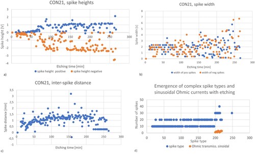
After ∼200 min the pore sizes have become too large for prompt pore closure after each spike emission so that pore closure becomes delayed, thus giving rise to subsequent short, small sinusoidal Ohmic currents, Figures (b) and (d) (see the orange dots near y = 0 that show up between ∼ 200 and 225 min). This “malfunction” of the previously properly working transient pore closure mechanism (which possibly is some rapid elastic relaxation of the swollen polymer matrix around the pores) is also responsible for more complex bimodal (double spikes with alternating polarity; symbolized by y = 20), trimodal (y = 30), or multi-modal (y = 40) spikes emitted. Finally, around 270 min, spike emission disappears abruptly.
Near the end of the spike emission, after ∼ 270 min etching, two huge positive and negative spikes emerge that exceed the applied external voltage of ± 2 V somewhat, Figure (a). As had been shown in earlier work (Citation5), this indicates that here, negative differential resistances are involved in the spike formation. Hence, if one would have “frozen in” this sample’s working state (by rapidly replacing the etchant with a neutral or acidic solution), one would have obtained an electronically active device for amplification and oscillation. This would have been the first representative device of “Liquid electronics with etched SLI-irradiated polymer foils” as a counterpart of “Liquid electronics with etched SHI-irradiated polymer foils” that had been developed a decade ago (Citation5).
Figure (b) (spike widths vs. etching time) illustrates that the spikes were already relatively well-synchronized from their beginning at ∼20 min (spike widths ∼2 sec). However thereafter, they diverged exponentially more and more within some upper and lower thresholds, indicating a growing loss of correlation with proceeding etching time. Both positive and negative spikes behave in the same way.
Above 150 to 200 min, spike widths even triple. This bimodal behavior (small widths → large widths) may reflect the same mechanism as proposed for the spike heights: 1. in the first etching stage (up to a depth of ∼ 5 µm or so), one deals with etching of narrow individual damage zones around the impinging ion’s trajectories; 2. thereafter the etching of the collective radiation-damaged zone starts, resulting from multiple damage overlapping. This stage is dominated by lateral expansion of the etched region within the polymer. The more open this internal damage network becomes, the longer it takes for charges to migrate outwards from this internal transient charge storage towards the outside, i.e. the more the spike width will grow.
The well-defined curve that emerges for the time intervals between two successive spikes, Figure (c), indicates that spike synchronization (see chapter 2.2) has indeed advanced considerably in this sample. The initially short spike-to-spike distances (∼ 10 s) rise rapidly up to ∼ 1 min etching time; and thereafter only very slowly, until above ∼190 min etching time (i.e. shortly before spike emission vanishes completely), they decrease again. In other words, the spike emission pulses occur at increasing infrasound frequencies, starting with ∼ 170 mHz, and finally decreasing to a nearly-constant ∼ 17 mHz.
Figure 7. Original measuring protocols of the measured transmission signals for sample CON21. Shown are cut-outs a) from 100.0 to 108.3 min after the onset of etching, and b) from 208,3 to 217.0 min after the onset of etching.
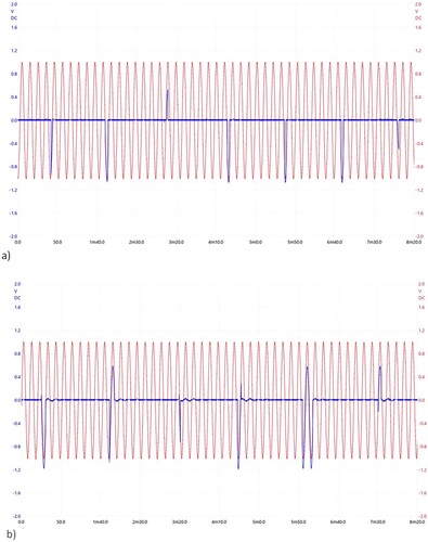
Figure 8. Overview of the physical spike parameters derived from the measurement of sample CON21. Primary correlations: (a) spike heights, (b) spike widths, and (c) the time interval between two successive spikes, as a function of the etching time. Finally, (d) schematically summarizes the emergence of increasingly more complex spike types (y = 10 → 40) and the emergence of short-time Ohmic currents during the progress of etching (y = 0). The value y = 10 describes single mono-modal spikes, y = 20 describes single bi-modal spikes, y = 30 corresponds to single tri-modal spikes, and y = 40 indicates even more complex multi-modal spike structures.
4.5. Sample CON23
The findings of this sample are again in striking contrast to the two former two examples. In this case, spike emission starts nearly simultaneously with the opening of conducting paths from one foil side to the other. From Figure (a), one can see that initially, this foil shows pronounced – in a few cases even perfect – rectification. However, in the transition regime, when the externally applied voltage changes from positive to negative, often (exclusively negative) spikes are triggered, which extend partly deep down, as if regular sinusoidal currents would extend without rectification. These spikes are emitted at roughly ∼ 40 Hz (for contrast, the applied external voltage operated at ∼ 6 Hz, hence ∼ 7 times slower). Usually, the spikes show up in sequences (similarly as for the sample CON1), however, the sequence width is strictly limited to the width of the negative half width of the applied sinusoidal voltage. I.e. in this case, a strong dependence of spike formation on the externally applied voltage holds indeed (see chapter 2.2). Again, times with pronounced spike formation alter with times where spikes are nearly absent. With proceeding etching, the height of the transmitted current increased, but the rectification worsened. The etching process was not recorded graphically much longer beyond Figure (b), and the spike emission ceased soon thereafter. These findings for the etching of foils with overlapping SLI resemble somewhat earlier findings on the etching of single SHI impacts on PET foils (Citation14, Citation36).
Figure 9. (a) Measuring protocol of sample CON23: (a) from 104,7 to 125 min, and (b) from 125 to 130,3 min. (a) The etchant breakthrough and onset of spike emission (blue) are nearly coincident, covering nearly exclusively only the negative sinusoidal half widths of the applied external voltage (red).
4.6. Sample CON33
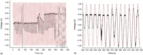
Similar effects as found for earlier examined SHI-irradiated and etched samples (Citation11, Citation17), where spike emission occurred only within one half-period of the externally applied sinusoidal voltage, were also found for sample CON33. Figure (a) gives an overview of the relatively short spike-emitting time interval of this sample before full etchant breakthrough with saturated Ohmic currents started; Figure (b) shows a closer detail of the spikes found in this case. This sample behaves again strikingly different from the others. First of all, it is characterized by an extremely fast etching progress; secondly, from the beginning of breakthrough on, this sample shows strong rectification, insofar as positive transmission signals are nearly always strongly suppressed. During this time, a multitude of tiny positive or negative narrow spikes with slightly less than 1 s width (average: 0.835 s) and heights between 0.01 and 0.09 V (average ∼ 0.025 V) emerge; they only vanish at t100%. Only during a few occasions was spike emission with negative transmission currents observed. This finding contrasts the previous one of sample CON23, where the region of spike emission was restricted to the region of negatively suppressed transmission currents. Furthermore, the whole transmission current spectrum is characterized by a very agitated baseline, created by overlapping chemical potentials that were transiently stepwise fluctuating. The rectification stems from a charge unbalance between both the foil’s cis- and the trans- sides; apparently, some positive ions (such as H+ and Na+ from H2O and NaOH, respectively) get bonded to the nanopore’s inner walls formed by etching, thus preventing ions of the same charge from their transmission across the nanoporous microbeam-irradiated region.Footnote2 In any case, the ionic attachment to the etched nanopores seems not to be very stable; occasional detaching allows small, positive charge spikes to get transmitted, and occasional additional attachment of more positive ions leads to spikes of the opposite polarity.
Figure 10. Measuring protocol of sample CON33; (a) overview of all the relevant etching time from 0 to about 450 seconds; Detailed view: (b) from 300 to 450 s. Spike emission (black) covers preferentially the positive sinusoidal half widths of the applied external voltage (red).
5. Discussion, Conclusions and Outlook
5.1. Discussion
Because we can now, for the first time, compare the earlier SHI results with the new SLI results, we understand that many of the spike observations are qualitatively consistent. But we also found, in some cases, strong differences between both results, which we cannot yet properly explain due to our current lack of knowledge about the details of the SLI-based nanostructures before and after etching. Therefore, we can, at present, only pose a number of new questions:
It is quite remarkable that these seemingly simple devices, such as small pieces of etched SLI-irradiated plastic, already contain autonomous electronic features of such amazing complexity, as the plethora of spikes and spike sequences constitute. How is this possible in more detail? Of course, we've only given a few rough answers in this article. But to get deeper, we should use AI-driven simulations to find out more precisely what allows the foils to behave in this way.
Another question concerns the synchronized spike emission frequencies. While a minimum spike emission frequency of around 2.65 Hz was found for SHI irradiation (i.e. the infrasound-to-sound transition region; see chapter 2.2 and (Citation14–18)), we recorded spike emission frequencies of ∼17 to 170 mHz, i.e. in the lower infrasound range, for spikes prepared by SLI irradiation, see Figure (c). Of course, this should be attributed to the much lower overlapping SLI’s deposited energy density available for the material’s destruction, and the different geometry of the damage distribution, than in the SHI case. But again, how to explain this in detail?
In the case of the SHI-irradiated and etched polymers (e.g. funnel-type etched tracks), we often found a strong abundance of capacitive and after-runner effects (Citation36). However, in the SLI-irradiated and etched foils, such effects were always absent. What is behind this difference?
Another interesting point: our present results suggest that there is no external triggering of the spike emission within one-half period of the applied external voltage. But what happens, if stronger signals are intentionally imposed onto these systems? Could they make possible some re-shaping of the behavior of the pulsating systems, i.e. could this multiparametric system be capable of learning how to behave differently?
5.2. Conclusion
A convenient way for intentionally introducing nanopores into an unstructured matrix is its irradiation with energetic ions and subsequent etching. Whereas high-energy heavy ions (SHI) form individual straight trails of massive damage (thus giving rise to straight broad nanopores after etching, which can be transformed into conducting wires or sensors), overlapping low-energy light ions (SLI) provide spatially extended 3D structures due to the considerable lateral scattering of the incident ions. These are expected to give rise to nanometric labyrinth-like cavern regions after etching, which may serve as ion reservoirs and regions of confined ion-ion interaction. The integration of neighbored unirradiated polymer regions into these structures makes it possible to exploit the polymer’s elastic and plastic properties for electric spike emitters, and probably also for other devices such as switches and volatile or permanent memory devices. The first proof of this claim was given some time ago by the production of SHI-irradiated devices. The subsequent claim that also etched overlapping SLI-irradiated polymer foils should be capable of overtaking similar tasks is now proven in this work, by the demonstration of SLI-based electric spike generators.
5.3. Outlook 1
This is what encourages us to now proceed to the next step, which is to understand the closer details of these nanostructures. For this reason,
the overall 3D depth distributions in the irradiated SLI-irradiated damage structures should be determined using incorporated markers;
the average width of the expected pores should be determined by incorporation of markers of different sizes;
for a better understanding of the electronic properties, it is also necessary to investigate the adhesion properties of the nanopore walls;
it is also necessary to find out what the suggested crazes and cracks in strained thin unirradiated polymer layers really look like, and how best to exploit them for electronic switching purposes;
AI-assisted model calculations should accompany the experimental findings. The aim is to optimize the irradiation and etching steps so that future production steps always provide spike-emitting samples;
in the future, it may be much cheaper to fabricate most ion-irradiated and etched electronically-active polymer devices using SLI instead of SHI. This can be a technology for the production of SLI-based resistors, capacitors, transistors, TEMPOS structures, biosensors, etc.
5.4. Outlook 2
Our general framework is oriented towards information processing. Even though information itself is an immaterial quantity, in practical applications, it requires a material carrier to be processed.
Currently, there are two concepts in our world for designing the carriers for information processing: “God’s technique”, common to all living matter (the use of organic molecules in well-defined working areas and migration paths, such as neurons and nerves in biological tissue), and human technology (by using electrons in semiconductor devices, such as transistors, ICs, and Cu wires). What is, however, still missing are new hybrid approaches to information processing that use both concepts. This is what our strategy aims at: considering the natural bioelectronic concept, we want to simulate these structures by letting ions in some carrier liquid (aqueous solutions) pass through the channels of a sophisticated structure in polymer matrices. Once such structures are proven to work reliably, they should be integrated either individually into modern semiconductor electronics (e.g. as sensors or actuators), or into biological species (as some kind of biocompatible prosthesesFootnote3), or combined with each other for complex data processing purposes. We expect that nanoporous structures in polymers may be able to take on the role of both active decision elements and passive connecting conductors by exploiting SHI and SLI-based etched polymers, as demonstrated in this work.
Acknowledgements
Financial support of this work from the GACR project No. 22-17346S is gratefully acknowledged. The measurements were carried out at the ‘CANAM’ infrastructure in NPI ASCR Rez. The authors also thank Mrs. S.A. Vacik for proofreading.
Disclosure statement
No potential conflict of interest was reported by the author(s).
Additional information
Funding
Notes on contributors
Jiri Vacik
Dr Jiri Vacik is an expert in nuclear analytical methods and materials science and a group leader, in the Nuclear Physics Institute, Czech Academy of Sciences, Rez, CR.
Dietmar Fink
Prof Dietmar Fink is a top expert in materials science, polymer science, nuclear analytical methods, informally in Nuclear Physics Institute, Czech Academy of Sciences, Rez, CR.
Giovanni Ceccio
Dr Giovanni Ceccio is a specialist in materials science, plasma physics and nuclear analytical methods, in the Nuclear Physics Institute, Czech Academy of Sciences, Rez, CR.
Vladimir Havranek
Dr Vladimir Havranek is an expert in nuclear analytical methods and materials science, a group leader in the Nuclear Physics Institute, Czech Academy of Sciences, Rez, CR.
Antonio Cannavo
Dr Antonio Cannavo is a specialist in materials science, plasma physics and nuclear analytical methods, Brookhaven National Laboratory, Upton, NY, USA.
Arnold Kiv
Prof Arnold Kiv is a top expert in materials science, polymer science, simulation and AI, Ben-Gurion University of the Negev, Israel.
Notes
1 Spike emission was also found when applying a voltage across the more complex, so-called TEMPOS-structures, which are based on insulator/semiconductor bilayer structures (such as SiO2/Si), where electronical anisotropy was subsequently imposed onto the insulating top layers by irradiating them with a beam of parallel SHIs, etching the formed SHI tracks in the top layers to create parallel nanopores, and finally inserting any conducting or semiconducting material (such as metallic or semiconducting nanoparticles, conducting polymers, fullerenes, etc.) into them, to make them electronically active. Also, semiconductor A/semiconductor B bilayer structures, so-called TEAMS-structures (such as metal oxide/Si) behave in the same way (with the metal oxide being, e.g. SnO2 or others); in this case, electronical anisotropy is again imposed by SHI irradiation of the top layer. However, as this layer is already semiconducting, neither subsequent etching nor insertion of additional materials is necessary to make these structures electronically active (Citation6–9). In this work, however, we will focus exclusively on the polymeric targets.
2 Note that in the previous example of sample CON23, we had observed rectification of (and spike emission from) the opposite side; i.e. in the latter example the dominantly affected ions must have been rather OH-, than the ions H+ and Na+ such as here. At present, it is still unclear what leads to this opposite behavior of both foils.
3 In this case, the prostheses could work with body liquids, and they could derive their power directly from chemical potential differences within the body. This would make them most user-friendly.
References
- Spohr, R. Ion Tracks and Microtechnology, Principles and Applications; K. Bethge Ed.; Springer, 1990, ISBN: 3528063300, 9783528063306.
- Dresselhaus, M.S.; Wassermann, B.; Wnek, E. Ion Implantation of Polymers. MRS Online Proc. Libr. 1983, 27, 413–422.
- Fink, D.; Gerardo Muñoz, H.; Alfonta, L.; Mandabi, Y.; Dias, J.F.; de Souza, C.T.; Bacakova, L.E.; Vacík, J.; Hnatowicz, V.; Kiv, A.E.; Fuks, D.; Papaleo, R.M. Status and Perspectives of Ion Track Electronics for Advanced Biosensing. Nanodevices Nanomaterials Ecol. Secur. NATO Sci. Peace Secur. B 2012, 2, 269–279. DOI:10.1007/978-94-007-4119-5_24.
- Fink, D.; Saad, A.; Dhamodaran, S.; Chandra, A.; Fahrner, W.; Hoppe, K.; Chadderton, L.T. Multiparametric Electronic Devices Based on Nuclear Tracks. Radiat. Meas. 2008, 43, S546–S551.
- Fink, D.; Kiv, A. The Nature of Negative Differential Resistance in SnO2-Si Structure. Comput. Model. New Technol. 2007, 11, 59–63.
- Fink, D.; Kiv, A.; Golovanov, V.; Chen, J.; Chandra, A.; Ivanovskaya, M.; Khirunenko, L.; Fuks, D. Tin Dioxide on Semiconductor as Material for New Electronics. J. Mater. Sci.: Mater. Electron. 2008, 19, 1222–1227.
- Fink, D.; Chadderton, L.T.; Kiv, A.; Saad, A.; Tabacnics, M.; de A. Rizutto, M.; Silva, A.d.O.D.; Fahrner, W.R.; Hoppe, K. Swift Heavy Ion Irradiation as a Tool for Creating Novel Nanoelectronic Structures. Radiat. Eff. Def. Solids 2007, 162, 543–551.
- Fink, D.; Chandra, A.; Fahrner, W.R.; Hoppe, K.; Winkelmann, H.; Saad, A.; Alegaonkar, P.; Berdinsky, A.; Grasser, D.; Lorenz, R. Ion Track-Based Electronic Elements. Vacuum 2008, 82, 900–905.
- Fink, D.; Kiv, A.; Fuks, D.; Saad, A.; Vacik, J.; Hnatowicz, V.; Chandra, A. Conducting Swift Heavy Ion Track Networks. Radiat. Eff. Def. Solids 2010, 165, 227–244.
- Kularatna, N. Power Electronic Design Handbook; Newnes: Boston, 1998; pp 232–233; ISBN:978-0750670733.
- Schulz, A.; Danziger, M.; Akapiev, G.N.; Trofimov, V.V.; Prokert, K. The Pore Opening Process of Etching PETP Films Irradiated by Multiply Heavy Ions and the Three-phase-model of the Etching Process of the Single ion Track. In Heavy Ion Physics; Oganessian, Y.T., Kalpakchieva, R., Eds.; World Scientific: Singapore, 1998; pp 792–795.
- Siwy, Z.S.; Powell, M.R.; Petrov, A.; Kalman, E.; Trautmann, C.; Eisenberg, R.S. Calcium-induced Voltage Gating in Single Conical Nanopores. Nano Lett. 2006, 6, 1729–1734.
- Graf, R.F. Modern Dictionary of Electronics, 7th ed.; Newnes: Boston, 1999; p 499; ISBN:978-0750698665.
- Fink, D.; Cruz, S.; Hernandez, G.M.; Kiv, A. Current Spikes in Polymeric Latent and Funnel-Type ion Tracks. Radiat. Eff. Def. Solids 2011, 166, 1–16.
- Fink, D.; Cruz, S.A.; Vacik, J.; Hnatowicz, V. Electrical Current Pulsations through Ion Irradiated Polymer Foils in Electrolytes. Radiat. Eff. Def. Solids 2010, 165, 818–833.
- Mykytenko, N.; Kiv, A.; Fink, D. Computer Modelling of Ion Current Pulsations in Track-containing Foils. J. Comput. Sci. 2015, 6, 34–39.
- Fink, D.; Kiv, A.; Fuks, D.; Munoz, G.H.; Cruz, S.A.; Fahrner, W.R.; Hoppe, K. Collective Interactions in Ion Track Electronics. Comput. Model. New Technol. 2011, 15, 7–18.
- Fink, D.; Muñoz, G.H.; Vacik, J.; Alfonta, L. Pulsed Biosensing. IEEE Sens. J. 2011, 11, 1084–1087.
- Mykytenko, N.; Fink, D.; Kiv, A. Generalized Model of Pulsating Track Devices. Comput. Model. New Technol. 2014, 18 (1), 7–12.
- Fink, D.; Muñoz, H.G.; Cruz, S.; Alfontal, L.; Mandabi, Y.; Vacík, J.; Hnatowicz, V.; Chandra, A. Electroactive Polymers as Obtained by Insertion of Electrolytes into Polymeric Tracks, In Electroactive Polymers: Materials and Devices, Vol. IV; Hashmi, S.A. et al., Eds.; Macmillan: New Delhi, 2012.
- Appleton, E.V. The Automatic Synchronization of Triode Oscillators. Proc. Camb. Philos. Soc. 1923, 21 (Part III), 231–248.
- de Bellescize, H. La reception synchrone. L’Onde Electrique/Revue de l’Electricite e de l’Electronicque 1932, 11, 230–240.
- Bernas, A.; Chambaudet, A. Sur les degats chimiques crees par des faisceaux d’electrons ou d’ions lourds dans different plastiques detecteurs de traces. Radiat. Eff. 1974, 22, 129–134.
- Boyett, R.H.; Johnson, D.R.; Becker, K. Some Studies of the Chemical Damage Mechanism Along Charge-Particle Tracks Ion Polymers. Radiat. Eff. 1970, 42, 1–12.
- Picq, V.; Ramillon, J.M.; Balanzat, E. Swift Heavy Ions on Polymers: Hydrocarbon gas Release. Nucl. Instr. Meth. 1998, B146, 496–503.
- Mittal, V.K.; Lotha, S.; Avasthi, D.K. Hydrogen Loss Under Heavy ion Irradiation in Polymers. Radiat. Eff. Def. Solids 1999, 147, 199–210.
- Marletta, G. Chemical Reactions and Physical Property Modifications Induced by keV ion Beams in Polymers. Nucl. Instr. Meth. 1990, B46, 295–305.
- Calcagno, L.; Compagni, G.; Foti, G. Structural Modifications of Polymer Films by ion Irradiation. Nucl. Instr. Meth. 1992, B65, 413–422.
- Steckenreiter, T.; Balanzat, E.; Fuess, H.; Trautmann, C. Chemical Modifications of PET Induced by Swift Heavy Ions. Nucl. Instr. Meth. 1997, B131, 159–166.
- Benton, E.V.; Henke, R.P. Sensitivity Enhancement of Lexan Nuclear Track Detector. Nucl. Instr. Meth. 1969, 70, 183–184.
- Venkatesan, T.; Forrest, S.R.; Kaplan, M.L.; Murray, C.A.; Schmidt, P.H.; Wilkens, B.J. Ion-beam Induced Conductivity in Polymer Films. J. Appl. Phys. 1983, 54, 3150–3153.
- Hioki, T.; Noda, S.; Sugiura, M.; Kakeno, M.; Yamada, K.; Kawamoto, J. Electrical and Optical Properties of ion-Irradiated Organic Polymer Kapton H. Appl. Phys. Lett. 1983, 43, 30–32.
- Venkatesan, T.; Calgano, L.; Elman, B.S.; Foti, G. Ion Beam Effects in Organic Molecular Solids and Polymers. In Mazzoldi, P., Arnold, G.W., Eds.; Ion Beam Modification of Insulators; Elsevier: Amsterdam; 1987; pp 301–379.
- Wang, Y.Q.; Giedd, R.E.; Moss, M.G.; Kaufmann, J. Electronic Properties of Ion Implanted Polymer Films. Nucl. Instr. Meth. 1997, B127/128, 710–715.
- Ziegler, J.F.; Biersack, J.P.; Littmark, U. The Stopping and Ranges of Ions in Solids, Vol 1.; Pergamon: Oxford, New York, 1985.
- Fink, D.; Vacik, J.; Hnatowicz, V.; Muñoz, H.G.; Alfonta, L.; Klinkovich, I. Funnel-type Etched Ion Tracks in Polymers. Radiation Eff. Def. Solids 2010, 165, 343–361.