
 ?Mathematical formulae have been encoded as MathML and are displayed in this HTML version using MathJax in order to improve their display. Uncheck the box to turn MathJax off. This feature requires Javascript. Click on a formula to zoom.
Abstract
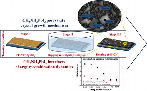
Although the two-step deposition (TSD) method is widely adopted for the high performance perovskite solar cells (PSCs), the CH3NH3PbI3 perovskite crystal growth mechanism during the TSD process and the photo-generated charge recombination dynamics in the mesoporous-TiO2 (mp-TiO2)/CH3NH3PbI3/hole transporting material (HTM) system remains unexploited. Herein, we modified the concentration of PbI2 (C(PbI2)) solution to control the perovskite crystal properties, and observed an abnormal CH3NH3PbI3 grain growth phenomenon atop mesoporous TiO2 film. To illustrate this abnormal grain growth mechanism, we propose that a grain ripening process is taking place during the transformation from PbI2 to CH3NH3PbI3, and discuss the PbI2 nuclei morphology, perovskite grain growing stage, as well as Pb:I atomic ratio difference among CH3NH3PbI3 grains with different morphology. These C(PbI2)-dependent perovskite morphologies resulted in varied charge carrier transfer properties throughout the mp-TiO2/CH3NH3PbI3/HTM hybrid, as illustrated by photoluminescence measurement. Furthermore, the effect of CH3NH3PbI3 morphology on light absorption and interfacial properties is investigated and correlated with the photovoltaic performance of PSCs.
1. Introduction
The scientific community has witnessed an unprecedented and unexpected technological advance in the field of photovoltaics brought about by the advent of an organometal halide perovskite material, CH3NH3PbX3 (X = Cl, Br, or I) [Citation1–7]. Significant progress in perovskite solar cells (PSCs) has been achieved in the past three years, and a certified power conversion efficiency (PCE) up to 22% has been recently reported [Citation8]. The stunning success to apply organometal halide perovskite in the context of photovoltaics would not have been realized without the optimization of highly crystallized perovskite layer. A desirable perovskite thin film would exhibit a complete surface coverage with no defects, a small surface roughness and a well-defined grain structure [Citation9–11]. Meanwhile, devices with mesoporous structure are widely investigated because of the minimized carrier drift and diffusion length [Citation12,13], which benefits from the direct electron injection from perovskite to electron-transporting materials (ETM). The electron transport layers in meso-structured devices usually employ wide bandgap semiconductors, such as TiO2 [Citation14,15], and ZnO [Citation16]; the crystallization of the perovskite material also benefits greatly from the enhanced nucleation at the meso-structure interfacial sites. In addition, insulators such as ZrO2[Citation17] or Al2O3[Citation18] are also applied as scaffold in PSCs, where the light induced electrons are generated and transported through the perovskite material itself and then injected to charge the selective layer directly.
Based on these fundamental architectures, versatile film formation technologies such as vacuum evaporation [Citation19], sequential deposition [Citation14], and vapor-assisted deposition[Citation20] were developed for efficient PSC fabrication. In these previous studies, a significant development in perovskite fabricating process is the two-step deposition (TSD) method, originally applied and developed by Liang and Burschka et al.[Citation14,21] The pre-formed PbI2 particles react with CH3NH3I in isopropanol solution via in situ insertion reaction, leading to full film coverage by CH3NH3PbI3 formation. This approach was proved to be effective in ensuring better repeatability by restraining the PbI2 crystals within the diameter of the TiO2 mesopores and facilitating the reaction with CH3NH3I. The TSD technique has been adopted by many groups for high-performance PSC fabrication, and various optimizations have been carried out through solution chemistry/processing modification, such as additive-effects on PbI2 solution [Citation22], retarding PbI2 crystallization using dimethyl sulfoxide solvent [Citation23] and PbI2 morphology optimization [Citation24–26]. Park et al. [Citation27] applied thermodynamics to correlate the crystal size with the concentration of CH3NH3I and reaction temperature. However, the exact perovskite crystal growth mechanism during the TSD and the detailed free charge recombination dynamics on the TiO2/perovskite interface or within the bulk of semiconductor remain unexploited. Moreover, controlling perovskite morphology is critical for developing high efficient devices. The coverage of perovskite film over mesoporous TiO2 film, perovskite crystallinity and surface roughness can dramatically affect the photoelectrochemical properties, such as light harvesting, charge carrier transport and charge dissolution across the interfaces [Citation28–30].
In this work, we report an abnormal CH3NH3PbI3 grain growth atop mesoporous TiO2 film during concentration variation of PbI2 (C(PbI2)) using TSD technique. Corresponding to different perovskite morphologies, the photo-generated charge recombination mechanism of the mesoporous-TiO2 (mp-TiO2)/CH3NH3PbI3/hole transporting materials (HTM) system is characterized by photoluminescence [Citation31] measurement. Typical C(PbI2)-dependent perovskite morphology shows a significant effect on the light-harvesting, interface properties and photovoltaic performance of the as-made PSCs.
2. Experimental section
2.1. Materials
All the solvents and reagents were used as received, including PbI2 (99%, Sigma-Aldrich, Darmstadt, Germany), hydroiodic acid (HI, 57 wt% in water, Sigma-Aldrich, Taiwan, China), methylamine (CH3NH2, 33 wt% in ethanol, Sigma-Aldrich), spiro-OMeTAD (Luminescence Technology Corp., Heysham, UK)), lithium bis(trifluoromethylsulfon)imide (LiTFSI, Alfa Aesar), 4-tert-butylpyridine (TBP, 96%, Sigma-Aldrich). Conductive fluorine-doped tin oxide glasses (FTO, sheet resistance of 15 Ω/ sq. Nippon Sheet Glass Co., Osaka, Japan) were applied as substrates.
2.2. Device fabrication
CH3NH3I was produced according to a published method [Citation32]. Briefly, CH3NH3I was synthesized by dropping HI into CH3NH2 solution at 0 °C under continuous stirring. By evaporating the ethanol at 100 °C, the precipitate was collected. Then the CH3NH3I powders were recrystallized from ethanol and washed with diethyl ether three times and finally dried in a vacuum oven before use.
FTO glasses were cleaned sequentially by ultra-sonication in detergent, deionized water, ethanol, acetone and isopropanol and dried with nitrogen and then cleaned by UV/ozone before use. A compact TiO2 blocking layer (bl-TiO2) was firstly deposited onto the surface of FTO substrate by spin-coating titanium isopropoxide in ethanol with HCl additives as hydrolysis inhibitor. The film was then sintered at 500 °C for 30 min [Citation33]. An mp-TiO2 layer was then fabricated by spinning TiO2 paste (Dyesol 18 NR-T, 18 nm average nanoparticle diameter) diluted in anhydrous ethanol (2:7 by weight) at 5000 rpm for 60 s. The layers were then sintered in the oven at 500 °C for 30 min. Prior to use, the films were again dried at 110 °C for 30 min to remove water.
A PbI2 solution in dimethylformamide (DMF; 0.6 M/ 0.8 M/ 1.0 M/ 1.2 M/ 1.4 M/ 1.6 M) was then deposited onto the mp-TiO2 film by spin-coating at 6000 rpm for 60 s. The PbI2 films were dried at 100 °C on a hotplate for 30 min. After gradually cooling to room temperature, the films were dipped in a 10 mg ml–1 CH3NH3I in iso-propanol solution for 20 min to obtain CH3NH3PbI3, rinsed with 2-propanol for 15 s and then dried at 100 °C in a vacuum oven for 30 min.
The HTM solution was prepared by dissolving 72.3 mg spiro-OMeTAD, 28.8 μl TBP and 17.5 μl of a solution of 520 mg ml–1 LiTFSI in acetonitrile into 1 ml anhydrous chlorobenzene. The FTO/bl-TiO2/mp-TiO2/CH3NH3PbI3 film was covered with HTM solution by spin-coating at 4000 rpm for 60 s. Devices were kept in a dry box (air humidity < 10%) for 10 h prior to thermal evaporation of 80 nm Au electrodes (under ~10−6 Torr vacuum, at a rate of ~ 6 nm min–1). All spin-coating operations were carried out in the air condition with a humidity of < 30%.
2.3. Film and device characterization
The surfaces and cross-sections of the samples were observed with a field emission scanning electron microscope (FESEM, LEO 1530 Gemini, Zeiss, Oberkochen, Germany). The crystal structure of the samples was characterized with a X-ray diffractometer (XRD, Bruker D8, Billerica, MA, USA) using Cu Kα radiation (1.54 Å). UV-vis reflectance and transmittance spectra were obtained by an UV/vis/NIR spectrophotometer (Lambda 950, Perkin-Elmer, Waltham, MA, USA) equipped with an integrating sphere module. To simulate the cells’ working condition, the monochromatic light was illuminated through the FTO side of samples. The incident photon to current efficiency (IPCE) was measured with a quantum efficiency characterization system (QEX10, PV measurements, Boulder, CO, USA). Prior to starting the measurement, a standard silicon solar cell as the reference was used to calibrate the spectra from 300 to 1000 nm. Steady-state and time-resolved PL spectra were both acquired with an optical spectrometer (FLS920, Edinburgh Instruments, Livingston, UK). The steady-state PL spectra were collected by illuminating the sample with a monochromatic light (λexc=460 nm, xenon lamp). The time-resolved PL spectra were acquired with samples excited by a pulsed laser beam (405 nm, 10 MHz, pulse duration of < 100 ps) under a time-correlated single photon counting (TCSPC) mode. PL lifetime was deduced by fitting the collected transient curves with a bi-exponential function as shown below:(1)
(1)
The current density-voltage (J−V) characteristics of the cells were collected under illumination of a solar simulator (AM 1.5, 1000 W/m2, Oriel, Irvine, CA, USA), calibrated with a standard silicon solar cell (Si PDS1337–1010BQ, Bunkoukeiki Co., Ltd., Tokyo, Japan) with a Keithley 2400 digital source meter (Keithley, Solon, OH, USA). The scanning voltage step during the measurement is 10 mV, and the dwell time at each voltage is 100 ms. Forward and backward scans were carried out between 1.2 V and –0.1 V.
3. Results and discussion
The FTO/bl-TiO2/mp-TiO2/CH3NH3PbI3 films with different morphologies were successfully fabricated by the typical TSD method with varied C(PbI2), ranging from 0.6 M to 1.6 M. Top-view SEM images of the samples are shown in Figure . It can be observed that the mp-TiO2 layer has been fully covered by the CH3NH3PbI3 layer (Figure (a), (b)) at all conditions, when a relatively high spinning speed (6000 rpm) for PbI2 solution was used. We also found that higher spinning speed is better for the homogeneous spreading of PbI2 on top of the mesoporous structure (Figure S1). The thickness of the PbI2 layer was gradually increased from 78 to 471 nm with the increased C(PbI2) of 0.6 M to 1.6 M, as shown in Figure S2. The PbI2 layer was of porous morphology at high C(PbI2) which was caused by the evaporation of excess DMF when annealing. When immersing PbI2 film into CH3NH3I solution, densely packed layers consisted of crystalline perovskite particles were formed, although the perovskite coverage seemed to be less complete when increasing the C(PbI2) up to 1.4 M and 1.6 M, which may be caused by the strong driving force of nucleation at such a high concentration and the non-uniform evaporation of DMF in the presence of thick capping layer [Citation34].
Figure 1. (a) FESEM top views of FTO/bl-TiO2/mp-TiO2 /CH3NH3PbI3 films fabricated with C(PbI2) of 0.6, 0.8, 1.0, 1.2, 1.4 and 1.6 M, (b) low magnification images of (a).
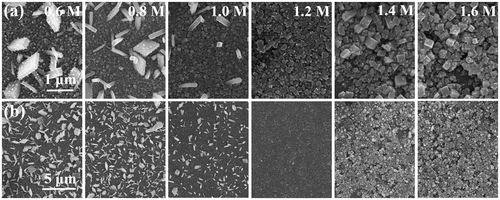
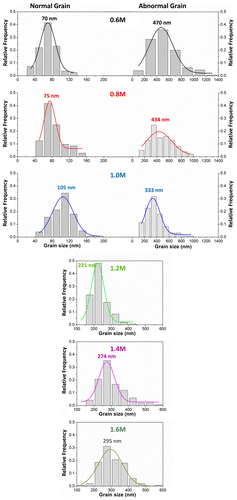
More importantly, we observed an abnormal grain growth of perovskite crystals, especially at low C(PbI2), with morphologies of nanocubes, nanoplates or nanorods, hundreds nanometers in size, randomly distributed on the mp-TiO2. The average grain size of the abnormally grown big crystals versus C(PbI2) was summarized in Figure , which revealed that the grain size distributions gradually centralized when C(PbI2) was increased from 0.6 M to 1.0 M. The abnormal crystals disappeared completely when C(PbI2) increased beyond 1.2 M, while the average crystal size increased from 221 to 274 and to 295 nm respectively at C(PbI2) of 1.2, 1.4 and 1.6 M, as determined by Gaussian fitting of the grain size distributions. We consider the abnormal perovskite grain growth at low C(PbI2) to be the result of the relatively high surface energy of small crystalline grains, which leads to crystalline grains growing or ‘ripening’ at the expense of others, so as to reduce grain boundary energy during the transformation of PbI2 to CH3NH3PbI3.
Figure 2. Statistical distributions and their Gaussian fitting (solid lines) of the CH3NH3PbI3 grain sizes determined from the FESEM images. For the samples of 0.6, 0.8 and 1.0 M, the grains with normal sizes and the abnormal grains were collected separately. No abnormal grain occurred in samples of 1.2, 1.4 and 1.6 M, so they showed only one peak in their size distributions.
As illustrated in Figure S3, we separate the abnormal grain grown process of CH3NH3PbI3 into three stages. During stage I, the spin-coated PbI2 layer at C(PbI2) of 0.8 M showed a homogeneous crystalline distribution with the absence of abnormally grown grains (Figure S3(a)). In stage II, the layered PbI2 structure, consisting of three spatially repeating planes (I–Pb–I) [Citation35], facilitates the insertion of the CH3NH3I to form the hybrid perovskite accompanied by a volume expansion from the originally edge-sharing octahedral structure to the corner-sharing octahedral structure in perovskite films [Citation36]. In the meantime, the abnormal grain growth occurred during this stage as we observed the existence of CH3NH3PbI3 crystals with a diameter of hundreds of nanometers (Figure S3(b)) when the samples were taken out of CH3NH3I solution without further annealing. We think that the abnormal grain growth may be driven by the reduction of boundary length, which helps to minimize the surface free energy. The abnormal grain growth is a grain ripening process, and this crystalline rearrangement often appears during polycrystalline film growth [Citation37]. Different PbI2 concentrations strongly affect the density of PbI2 nuclei at Stage I and further on the kinetic process of perovskite nucleation in the initial transforming stages. Meanwhile, the broad distribution of grain size especially at low C(PbI2) may also contribute to the local concentration differences, which thus resulted in the diffusion-controlled mass transport and gave rise to an abnormal grain growth [Citation37]. As an evidence of the concentration difference, we characterized the element composition of the normal CH3NH3PbI3 crystals and the abnormal ones with different morphologies using energy dispersive spectroscopy (EDS) measurement in SEM as shown in Figure S4. The Pb:I atomic ratios were 1:2.80 ± 0.20, 1:2.82 ± 0.14 and 1:2.77 ± 0.12 for abnormal big-size CH3NH3PbI3 crystals with shapes like nanocubes, nanoplates and nanorods respectively, which showed that the I vacancy or I substituted by Pb occurred in the big-size crystals comparing to the ideal 1:3 ratio of Pb:I atom for CH3NH3PbI3 crystal. As for the normal CH3NH3PbI3 crystals with size of 50–100 nm, a Pb:I atomic ratio of 1:3.39 ± 0.31 was found. The significant difference of Pb:I atomic ratio in different CH3NH3PbI3 crystal morphologies proved the mass transport effect on the abnormal grain growth. As for C(PbI2) over 1.2 M, the PbI2 reactant and the density of nuclei of perovskite grains are sufficient enough to form a homogenous perovskite capping layer with a narrow distribution of grain size. Stage III is the annealing process, during which the residual solvent evaporated and the CH3NH3PbI3 crystals grew further. As shown in Figure S3(c) and S3(d), the integral CH3NH3PbI3 morphology did not significantly change, in spite of a slight grain growth during annealing time of 30 min at 100 °C.
The optical properties of the perovskite films with typical C(PbI2)-dependent morphologies and as-made devices were characterized as shown in Figure S5, including the transmittance (T), reflectance (R) and absorbance (A) of FTO/bl-TiO2/mp-TiO2/CH3NH3PbI3 films. Absorbance was calculated as A=1 – T – R.
PbI2 films with typical yellow color (Figure S5, inset) turned darker and more opaque with PbI2 concentration increasing from 0.6 M to 1.6 M. Meanwhile, the as-prepared CH3NH3PbI3 films exhibit strong light absorption from 350 to 780 nm, whereas the light absorption is relatively weak from 550 to 780 nm, indicating inadequate light harvesting (Figure S5(c)). Notably, the absorbance of the FTO/bl-TiO2/mp-TiO2 /CH3NH3PbI3 film increased significantly from 0.6 to 1.2 M, and reached a plateau when C(PbI2) was 1.2 M, where the abnormal big-size crystals disappeared completely (Figure ). However, when the concentration was further increased to 1.6 M, a slight increase of absorbance occurred, which could be attributed to the thickening of the perovskite capping layer, as illustrated in Figure .
The charge separation and transport in perovskite layers happened when the free electrons were excited to the conduction band of perovskite by the absorption of light, which was then investigated by the steady-state and time-resolved PL measurement associated with C(PbI2)-dependent morphologies. An emission peak around 770 nm was detected for all the samples. We found that the PL intensity decreased when increasing C(PbI2) from 0.6 M to 1.6 M (Figure (a)), despite more perovskite loading at higher C(PbI2). This is in stark contrast to the work by Bi et al. [Citation25] where the weak PL emission indicates a lower amount of perovskite. The less light absorption for lower amount of perovskite observed by Bi et al. indicates that a portion of the exciting light is scattered elsewhere. This should result in sample-dependent light absorption, whereas we believe that PL intensity reflects the real recombination mechanisms in perovskite films only when the exciting light is equally absorbed by the samples. For samples of 1.0 to 1.6 M, we could find the complete absorption of the exciting light of 460 nm (as shown in Figure S5(c)), so that the lower PL emission at higher C(PbI2) indicated a larger quenching efficiency of photo-generated charges corresponding to a more effective electron injection across the interface between TiO2 and perovskite. The sample of 0.6 M, with inadequate absorption of 460 nm light (Figure S5(c)), however showed very strong PL emission. This further proved the lower quenching efficiency at lower C(PbI2). It is worth noting that the PL decline may also due to the intrinsic light emission behavior of the samples with different C(PbI2). In bare semiconductor film, the PL intensity will be affected by the non-radiative recombination at energetically favored sites such as discrete defect and impurity sites at interfaces and within the bulk of the material [Citation38]. However, the effect of crystal morphology and defect on the perovskite PL intensity is still unclear. The PL intensity varied a lot even for the different crystals in one perovskite film as shown in the PL mapping measurement given by de Quilettes et al. [Citation39]. The discussion on the time-resolved PL spectra in the following text also illustrates the quenching effect of the interface between ETM and perovskite.
Figure 3. (a) Steady-state PL spectra and (b) XRD patterns of FTO/bl-TiO2/mp-TiO2 /CH3NH3PbI3 films as a function of C(PbI2).
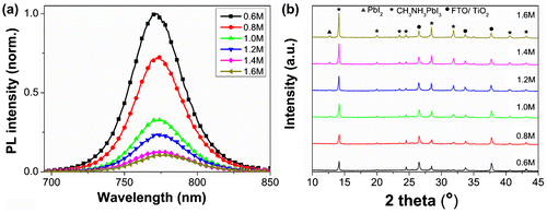
The XRD patterns of the CH3NH3PbI3 using different C(PbI2) were also characterized, and are shown in Figure (b). The strong Bragg peaks at 14.08, 28.41, 31.85, and 43.19° can be assigned to (110), (220), (310), and (330) planes of the CH3NH3PbI3 phase, which is in good agreement with literature data corresponding to a tetragonal I4 cm crystal structure of halide perovskite [Citation40]. A small peak at 12.65° was identified for the samples above 1.0 M, which belongs to the (001) lattice plane of PbI2, indicating incomplete phase conversion [Citation14], which could be attributed to the PbI2 layer becoming more compact when C(PbI2) is higher than 1.0 M [Citation25]. Such PbI2 impurity has been widely observed even in highly efficient devices reported by other groups, which was claimed to have a positive effect on the cell performance by passivating the perovskite layers [Citation41].
To further analyze the steady-state PL measurements and investigate the quenching efficiency of these C(PbI2)-dependent morphologies, time-resolved PL spectra (Figure (a)) were characterized. It has been demonstrated that there are two general mechanisms for recombination in bare CH3NH3PbI3 thin films, which can be described by a rate equation:(2)
(2)
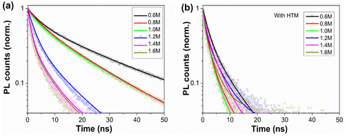
Figure 4. Time-resolved PL spectra of (a) FTO/bl-TiO2/mp-TiO2 /CH3NH3PbI3 films and (b) FTO/bl-TiO2/mp-TiO2/CH3NH3PbI3/HTM films as a function of C(PbI2).
where n is the excited carrier density, A and B represent the single-carrier trapping rate and the two-carrier radiative recombination coefficient, respectively [Citation42,43]. In particular, the origin of the PL is driven by a radiative two-carrier (non-geminate) recombination process involving electrons and holes [Citation38,44]. In bare semiconductor film, the carrier trapping dynamics is dominated by non-radiative recombination at energetically favored sites such as impurity sites and discrete defect at the bulk and interfaces of the material. Meanwhile, in the FTO/bl-TiO2/mp-TiO2/CH3NH3PbI3 film, the interface between TiO2 and CH3NH3PbI3 capping layer would lead to a strong decrease of the PL intensity by band bending at the interface, which can form a depletion region where charges are effectively quenched [Citation45,46].
In our work, the PL lifetime was fitted with a bi-exponential function including a fast decay at early times followed by a slow decay process. When the photocarrier density (n) is large enough, in which condition discrete defect and impurity sites are saturated and the radiative rate is fast, the effective PL lifetime derived from Equation (Equation3(3)
(3) ) can be approximately written as:[Citation45]
(3)
(3)
This expression reproduces well the related parameters of PL decay shown in Table S1. It should be noticed that the laser beam of 405 nm with maximum fluence used here was strong enough to saturate the intermediate states and fully penetrate the perovskite films. We believe that the fast decay process is the result of radiative decay, which is strongly n-dependent as illustrated in Equation (Equation3(3)
(3) ), reflecting the quenching efficiency of band bending at the interface. And the slow decay process is the result of carrier trapping mechanism, reflecting the non-radiative recombination via intermediate states [Citation40]. For the samples of 0.6 M to 1.6 M, the radiative decay lifetime (τ1) gradually decreased from 4.57 to 1.24 ns (Figure ), which indicated a more effective charge dissociation at higher C(PbI2). As evidenced in Figures and (b), the increase of C(PbI2) centralized grain size distributions and improved the crystallinity of the perovskite thin films, facilitating the free carrier diffusion and enhancing the charge quenching efficiency.
Figure 5. The radiative decay lifetime (τ1) determined by fitting the time-resolved PL spectra of FTO/bl-TiO2/mp-TiO2/CH3NH3PbI3 film with or without an HTM layer as a function of C(PbI2).
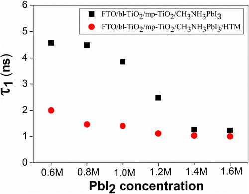
To identify whether the charge quenching efficiency is complete at the TiO2/CH3NH3PbI3 interface, and to probe the charge recombination behavior in real devices, a spiro-OMeTAD HTM film containing LiTFSI and TBP dopants was fabricated onto the CH3NH3PbI3 capping layer and the corresponding PL decay was characterized (Figure (b)). The existence of an HTM layer atop the perovskite significantly facilitated the fast radiative recombination rate from 4.57 ns to 2.00 ns of sample of 0.6 M (Figure and Table S1), indicating strong quenching efficiency at the interface between CH3NH3PbI3 and HTM layer, which was also demonstrated by Xing et al. [Citation47] and Stranks et al. [Citation33]. This suggests that the photo-generated free charges have not been fully quenched by the TiO2/CH3NH3PbI3 interface at C(PbI2) of 0.6 M. For sample of 1.4 M, the fast decay lifetime decreased from 1.26 ns to 1.03 ns after adding an HTM layer. This little variation in the fast decay lifetime indicated that the charge quenching was mostly completed at the TiO2/CH3NH3PbI3 interface. It could explain the high efficiency of hole conductor-free CH3NH3PbI3/TiO2 heterojunction solar cells [Citation48,49]. The slow decay process (τ2) representing carrier trapping mechanism was not analyzed here since the non-radiative recombination via intermediate states was strongly influenced by the crystallinity, discrete defect, impurity sites and film thickness of the CH3NH3PbI3 thin films.
The photovoltaic performance for perovskite solar cells with typical C(PbI2)-dependent morphologies are shown in Figure and the detailed J−V characteristics of studied solar cells are tabulated in Table S2. To assure reliability in the measurements, at least eight devices at each condition were investigated. When 0.6 M PbI2 was used, the PCE was rather poor (~1%). By increasing the concentration of PbI2, the efficiency was first improved to 12.0% at C(PbI2) of 1.2 M, and then decreased to 9.4%. The best performance of 12.6% was obtained at C(PbI2) of 1.2 M with a short-circuit photocurrent density (Jsc) of 20.8 mA cm–2, an open-circuit Voltage (Voc) of 947 mV, and a fill factor (FF) of 0.64, respectively. The Jsc, Voc and FF performed the same trend as the PCE. In particular, Jsc first improved from 3.6 to 19.7 mA cm–2 when the C(PbI2) increased from 0.6 to 1.2 M, which is consistent with the enhanced absorption shown in Figure S5. Meanwhile, at low C(PbI2) the insufficient charge carrier extraction across this heterogeneous interface as illustrated in PL decay measurement would cause a poor charge collection efficiency and further lead to a drop of Jsc. However, further increasing C(PbI2) from 1.2 to 1.6 M reduced Jsc from 19.7 to 15.8 mA cm–2 despite the enhanced absorption. This was attributed to the reduced perovskite coverage and the rough surface at high C(PbI2) as shown in Figure , which indicated a less effective charge collection. IPCE spectra of the devices were tested from 300 nm to 830 nm as shown in Figure S6, and the integrated current density derived from the IPCE spectra corresponded well to the measured value from J−V measurement under simulated sunlight. It is worth noting that the great enhancement of IPCE spectra from 1.0 M to 1.2 M was supposed to be caused by the increased charge transporting efficiency across the device. The optical absorbance of 1.2 M perovskite film was very close to that of 1.2 M as shown in Figure S5(c), which indicated that the fairly equal amount of photogenerated charges were produced in the 1.0 and 1.2 M device. Furthermore, the increased charge transporting efficiency benefited from the smooth perovskite film produced by the disappearance of abnormal big perovskite crystals and also the increased thickness of perovskite layer [Citation50].
Figure 6. (a) J–V curves (under AM 1.5 G illumination of 1000 W m–2 intensity, active area of 6 mm2) as a function of C(PbI2). (b) A comparison of photovoltaic parameters of devices exhibiting C(PbI2)-dependent morphologies. The half-black dots inside the box show the average values of all the samples.
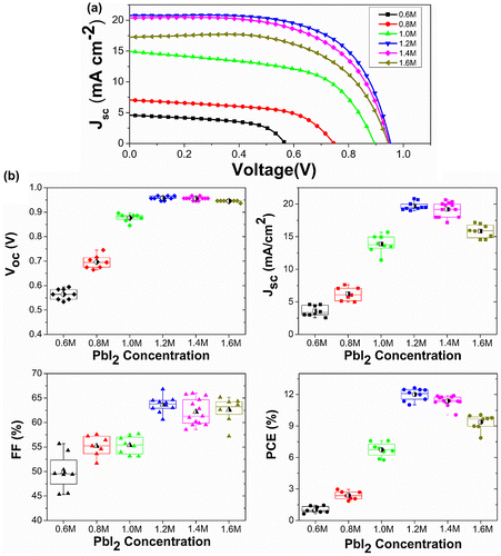
Voc increased steadily from 564 to 957 mV when C(PbI2) increased from 0.6 to 1.2 M. The low Voc indicates a charge recombination across the interface between ETM, CH3NH3PbI3 and HTM [Citation51]. According to the J−V data shown in Figure and Table S2, the Voc decreased gradually from 957 to 945 mV when increasing C(PbI2) from 1.2 M to 1.6 M. The Voc decline trend is furthermore confirmed by the large amount of devices been made. The Voc decrease revealed more serious charge recombination at higher C(PbI2) above 1.2 M, which also contributed to decrease Jsc. As evidenced in Figure , the abnormal grain growth of perovskite crystal (~400 nm) especially at low C(PbI2) is attributed to an ultra-rough perovskite surface, which would be difficult for the HTM layer to fully cover the capping layer, leading to direct contact of CH3NH3PbI3 and Au. The J−V curves under different scan directions are shown in Figure S7. The hysteresis phenomena appeared in our measurement, which was common in not only planar structural PSCs but also mesoporous structural devices. Some groups demonstrated that the hysteresis phenomenon was strongly affected by perovskite crystal size, mesoporous TiO2 morphology and the thickness of perovskite capping layer [Citation52–54], which had been speculated to originate from changes in absorber or contact conductivity, trapping/de-trapping of charge carriers, instinct ferroelectricity or ion migration [Citation55,56]. Despite the hysteresis, the PCE of cells at different C(PbI2) showed similar trends under forward scanning directions when comparing with the backward scanning data.
With comprehensive characterization combining FESEM, UV-vis, XRD, steady and time-resolved PL and J–V scans, we can see that a pinhole-free CH3NH3PbI3 capping layer with centralized grain sizes is critical for sufficient light absorption, achieving good interface properties by adequately extracting photo-generated free charges and obtaining an excellent photovoltaic performance. Extraordinarily big CH3NH3PbI3 crystals are harmful for the holistic crystallinity and the film smoothness, and will lead to a decrease of charge collecting efficiency by the recombination of transporting electrons and holes.
4. Conclusions
The abnormal grain growth of CH3NH3PbI3 crystals by a TSD method was observed at a low concentration of PbI2 precursor. We propose that a grain ripening process takes place during the transformation from PbI2 to CH3NH3PbI3: the relatively high surface energy of small crystalline grains results in that grains grow or ‘ripen’ at the expense of other ones accompanied with non-uniform elements distribution. Photo-generated charge recombination dynamics in CH3NH3PbI3 film was clearly illustrated by a recombination model, showing that the charge dissociation efficiency quenched by the interface between CH3NH3PbI3 and TiO2 was enhanced when increasing C(PbI2). The PCE of the devices was first improved from 0.6 to 1.2 M and then decreased, consisting of the variation of perovskite grain growth and morphology. The pinhole-free CH3NH3PbI3 capping layer with centralized grain sizes is crucial for harvesting sufficient light and achieving good interface properties and photovoltaic performance.
Disclosure statement
No potential conflict of interest was reported by the authors.
Supplemental data
Supplemental material is linked to the article DOI online at http://dx.doi//10.1080/14686996.2017.1298974.
Funding
The authors acknowledge the financial support provided by the Projects of International Cooperation and Exchanges NSFC [51561145007] and the Ministry of Science & Technology, P.R.China: Sino-Italy International Cooperation on Innovation [2016YFE0104000].s
Supplementary_Materials_Hong_Lin.pdf
Download PDF (1.3 MB)Related Research Data
References
- Wang B, Xiao X, Chen T. Perovskite photovoltaics: a high-efficiency newcomer to the solar cell family. Nanoscale. 2014;6:12287–12297.10.1039/C4NR04144E
- Yin W-J, Shi T, Yan Y. Unique properties of halide perovskites as possible origins of the superior solar cell performance. Adv Mater. 2014;26:4653–4658.10.1002/adma.v26.27
- Zhou H, Chen Q, Li G, et al. Interface engineering of highly efficient perovskite solar cells. Science. 2014;345:542–546.10.1126/science.1254050
- Perovskite fever. Nat Mater. 2014;13:837.
- McGehee MD. Perovskite solar cells: continuing to soar. Nat Mater. 2014;13:845–846.10.1038/nmat4050
- Kim H-S, Im SH, Park N-G. Organolead halide perovskite: new horizons in solar cell research. J Phy Chem C. 2014;118:5615–5625.10.1021/jp409025w
- Kim H-S, Lee C-R, Im J-H, et al. Lead iodide perovskite sensitized all-solid-state submicron thin film mesoscopic solar cell with efficiency exceeding 9%. Sci Rep. 2012;2:591.
- Best ResearchCell Efficiencies http://www.nrel.gov/ncpv/images/efficiency_chart.jpg
- Liang P-W, Liao C-Y, Chueh C-C, et al. Additive enhanced crystallization of solution-processed perovskite for highly efficient planar-heterojunction solar cells. Adv Mater. 2014;26:3748–3754.10.1002/adma.v26.22
- Chen C-W, Kang H-W, Hsiao S-Y, et al. Efficient and uniform planar-type perovskite solar cells by simple sequential vacuum deposition. Adv Mater. 2014;26:6647–6652.10.1002/adma.v26.38
- You J, Hong Z, Yang Y, et al. Low-temperature solution-processed perovskite solar cells with high efficiency and flexibility. ACS Nano. 2014;8:1674–1680.10.1021/nn406020d
- Im J-H, Jang I-H, Pellet N, et al. Growth of CH3NH3PbI3 cuboids with controlled size for high-efficiency perovskite solar cells. Nat Nano. 2014;9:927–932.10.1038/nnano.2014.181
- Lee MM, Teuscher J, Miyasaka T, et al. Efficient hybrid solar cells based on meso-superstructured organometal halide perovskites. Science. 2012;338:643–647.10.1126/science.1228604
- Burschka J, Pellet N, Moon S-J, et al. Sequential deposition as a route to high-performance perovskite-sensitized solar cells. Nature. 2013;499:316–319.10.1038/nature12340
- Noh JH, Im SH, Heo JH, et al. Chemical management for colorful, efficient, and stable inorganic–organic hybrid nanostructured solar cells. Nano Lett. 2013;13:1764–1769.10.1021/nl400349b
- Bi D, Boschloo G, Schwarzmüller S, et al. Efficient and stable CH3NH3PbI3-sensitized ZnO nanorod array solid-state solar cells. Nanoscale. 2013;5:11686–11691.10.1039/c3nr01542d
- Bi D, Moon S-J, Häggman L, et al. Using a two-step deposition technique to prepare perovskite (CH3NH3PbI3) for thin film solar cells based on ZrO2 and TiO2 mesostructures. RSC Adv. 2013;3:18762–18766.10.1039/c3ra43228a
- Ball JM, Lee MM, Hey A, et al. Low-temperature processed meso-superstructured to thin-film perovskite solar cells. Energy Environ Sci. 2013;6:1739–1743.10.1039/c3ee40810h
- Liu M, Johnston MB, Snaith HJ. Efficient planar heterojunction perovskite solar cells by vapour deposition. Nature. 2013;501:395–398.10.1038/nature12509
- Chen Q, Zhou H, Hong Z, et al. Planar Heterojunction Perovskite Solar Cells via Vapor-Assisted Solution Process. J Am Chem Soc. 2014;136:622–625.10.1021/ja411509g
- Liang K, Mitzi DB, Prikas MT. Synthesis and characterization of organic−inorganic perovskite thin films prepared using a versatile two-step dipping technique. Chem Mater. 1998;10:403–411.10.1021/cm970568f
- Docampo P, Hanusch FC, Stranks SD, et al. Solution deposition-conversion for planar heterojunction mixed halide perovskite solar cells. Adv Energy Mater. 2014;4.
- Wu Y, Islam A, Yang X, et al. Retarding the crystallization of PbI2 for highly reproducible planar-structured perovskite solar cells via sequential deposition. Energy Environ Sci. 2014;7:2934–2938.10.1039/C4EE01624F
- Li N, Dong H, Dong H, et al. Multifunctional perovskite capping layers in hybrid solar cells. J Mater Chem A. 2014;2:14973–14978.10.1039/C4TA02921F
- Bi DQ, El-Zohry AM, Hagfeldt A, et al. Unraveling the effect of PbI2 concentration on charge recombination kinetics in perovskite solar cells. ACS Photonics. 2015;2:589–594.10.1021/ph500255t
- Ko H-S, Lee J-W, Park N-G. 15.76% efficiency perovskite solar cells prepared under high relative humidity: importance of PbI2 morphology in two-step deposition of CH3NH3PbI3. J Mater Chem A. 2015;3:8808–8815.10.1039/C5TA00658A
- Ahn N, Kang SM, Lee J-W, et al. Thermodynamic regulation of CH3NH3PbI3 crystal growth and its effect on photovoltaic performance of perovskite solar cells. J Mater Chem A. 2015;3:19901–19906.10.1039/C5TA03990H
- Dualeh A, Tétreault N, Moehl T, et al. Effect of annealing temperature on film morphology of organic-inorganic hybrid pervoskite solid-state solar cells. Adv Funct Mater. 2014;24:3250–3258.10.1002/adfm.201304022
- Zhao YX, Zhu K. Solution chemistry engineering toward high-efficiency perovskite solar cells. J Phys Chem Lett. 2014;5:4175–4186.10.1021/jz501983v
- Xiao Z, Dong Q, Bi C, et al. Solvent Annealing of Perovskite-Induced Crystal Growth for Photovoltaic-Device Efficiency Enhancement. Adv Mater. 2014;26:6503–6509.10.1002/adma.201401685
- Yang B, Dyck O, Poplawsky J, et al. Perovskite solar cells with near 100% internal quantum efficiency based on large single crystalline grains and vertical bulk heterojunctions. J Am Chem Soc. 2015;137:9210–9213.10.1021/jacs.5b03144
- Im J-H, Lee C-R, Lee J-W, et al. 6.5% efficient perovskite quantum-dot-sensitized solar cell. Nanoscale. 2011;3:4088–4093.10.1039/c1nr10867k
- Stranks SD, Eperon GE, Grancini G, et al. Electron-hole diffusion lengths exceeding 1 micrometer in an organometal trihalide perovskite absorber. Science. 2013;342:341–344.10.1126/science.1243982
- Chernov AA. Stability of faceted shapes. J Cryst Growth. 1974;24-25:11–31.10.1016/0022-0248(74)90277-2
- Beckmann PA. A review of polytypism in lead iodide. Cryst Res Technol. 2010;45:455–460.10.1002/crat.201000066
- Baikie T, Fang Y, Kadro JM, et al. Synthesis and crystal chemistry of the hybrid perovskite (CH3NH3)PbI3 for solid-state sensitised solar cell applications. J Mater Chem A. 2013;1:5628–5641.10.1039/c3ta10518k
- Ohring M. Chapter 7 - Substrate surfaces and thin-film nucleation. In: Ohring M, editor. Materials Science of Thin Films. 2nd ed. San Diego, CA: Academic Press; 2002. p. 357–415.10.1016/B978-012524975-1/50010-0
- Saba M, Cadelano M, Marongiu D, et al. Correlated electron–hole plasma in organometal perovskites. Nat Commun. 2014;5:5049.10.1038/ncomms6049
- de Quilettes DW, Vorpahl SM, Stranks SD, et al. Impact of microstructure on local carrier lifetime in perovskite solar cells. Science. 2015;348:683–686.10.1126/science.aaa5333
- Stoumpos CC, Malliakas CD, Kanatzidis MG. Semiconducting tin and lead iodide perovskites with organic cations: phase transitions, high mobilities, and near-infrared photoluminescent properties. Inorg Chem. 2013;52:9019–9038.10.1021/ic401215x
- Cao DH, Stoumpos CC, Malliakas CD, et al. Remnant PbI2, an unforeseen necessity in high-efficiency hybrid perovskite-based solar cells?a). APL Mater. 2014;2:091101.10.1063/1.4895038
- D’Innocenzo V, Srimath Kandada AR, De Bastiani M, et al. Tuning the light emission properties by band gap engineering in hybrid lead halide perovskite. J Am Chem Soc. 2014;136:17730–17733.10.1021/ja511198f
- Yamada Y, Nakamura T, Endo M, et al. Photocarrier recombination dynamics in perovskite CH3NH3PbI3 for solar cell applications. J Am Chem Soc. 2014;136:11610–11613.10.1021/ja506624n
- Stranks SD, Burlakov VM, Leijtens T, et al. Recombination kinetics in organic-inorganic perovskites: excitons, free charge, and subgap states. Phys Rev Appl. 2014;2:034007.10.1103/PhysRevApplied.2.034007
- Gfroerer TH. Photoluminescence in analysis of surfaces and interfaces. encyclopedia of analytical chemistry. Hoboken: Wiley; 2006.
- De Bastiani M, D’Innocenzo V, Stranks SD, et al. Role of the crystallization substrate on the photoluminescence properties of organo-lead mixed halides perovskites. APL Mater. 2014;2:081509.10.1063/1.4889845
- Xing G, Mathews N, Sun S, et al. Long-range balanced electron- and hole-transport lengths in organic-inorganic CH3NH3PbI3. Science. 2013;342:344–347.10.1126/science.1243167
- Etgar L, Gao P, Xue Z, et al. Mesoscopic CH3NH3PbI3/TiO2 heterojunction solar cells. J Am Chem Soc. 2012;134:17396–17399.10.1021/ja307789s
- Hao F, Stoumpos CC, Liu Z, et al. Controllable perovskite crystallization at a gas-solid interface for hole conductor-free solar cells with steady power conversion efficiency over 10%. J Am Chem Soc. 2014;137:10399–10405.
- Yin X, Yao Z, Luo Q, et al. High efficiency inverted planar perovskite solar cells with solution-processed NiOx hole contact. ACS Appl Mater Interfaces. 2016;9:2439–2448.
- Arianna M, Joël T, Dennis F, et al. Unravelling the mechanism of photoinduced charge transfer processes in lead iodide perovskite solar cells. Nat Photonics. 2014;8:250–255.
- Wei J, Zhao Y, Li H, et al. Hysteresis analysis based on the ferroelectric effect in hybrid perovskite solar cells. J Phys Chem Lett. 2014;5:3937–3945.10.1021/jz502111u
- Chen H-W, Sakai N, Ikegami M, et al. Emergence of hysteresis and transient ferroelectric response in organo-lead halide perovskite solar cells. J. Phys Chem Lett. 2014;164–169.
- Kim H-S, Park N-G. Parameters affecting I-V hysteresis of CH3NH3PbI3 perovskite solar cells: effects of perovskite crystal size and mesoporous TiO2 layer. J Phys Chem Lett. 2014;5:2927–2934.10.1021/jz501392m
- Unger EL, Hoke ET, Bailie CD, et al. Hysteresis and transient behavior in current-voltage measurements of hybrid-perovskite absorber solar cells. Energy & Environmental Science. 2014;7:3690–3698.
- Zhang Y, Liu M, Eperon GE, et al. Charge selective contacts, mobile ions and anomalous hysteresis in organic-inorganic perovskite solar cells. Mater Horiz. 2015;2:315–322.10.1039/C4MH00238E