Abstract
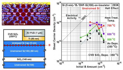
The atomic-layer (AL) doping technique in epitaxy has attracted attention as a low-resistive ultrathin semiconductor film as well as a two-dimensional (2-D) carrier transport system. In this paper, we report carrier properties for B AL-doped Si films with suppressed thermal diffusion. B AL-doped Si films were formed on Si(100) by B AL formation followed by Si cap layer deposition in low-energy Ar plasma-enhanced chemical-vapor deposition without substrate heating. After fabrication of Hall-effect devices with the B AL-doped Si films on unstrained and 0.8%-tensile-strained Si(100)-on-insulator substrates (maximum process temperature 350°C), carrier properties were electrically measured at room temperature. Typically for the initial B amount of 2 × 1014 cm−2 and 7 × 1014 cm−2, B concentration depth profiles showed a clear decay slope as steep as 1.3 nm/decade. Dominant carrier was a hole and the maximum sheet carrier densities as high as 4 × 1013 cm−2 and 2 × 1013 cm−2 (electrical activity ratio of about 7% and 3.5%) were measured respectively for the unstrained and 0.8%-tensile-strained Si with Hall mobility around 10–13 cm2 V−1 s−1. Moreover, mobility degradation was not observed even when sheet carrier density was increased by heat treatment at 500–700 °C. There is a possibility that the local carrier (ionized B atom) concentration around the B AL in Si reaches around 1021 cm−3 and 2-D impurity-band formation with strong Coulomb interaction is expected. The behavior of carrier properties for heat treatment at 500–700 °C implies that thermal diffusion causes broadening of the B AL in Si and decrease of local B concentration.