
 ?Mathematical formulae have been encoded as MathML and are displayed in this HTML version using MathJax in order to improve their display. Uncheck the box to turn MathJax off. This feature requires Javascript. Click on a formula to zoom.
ABSTRACT
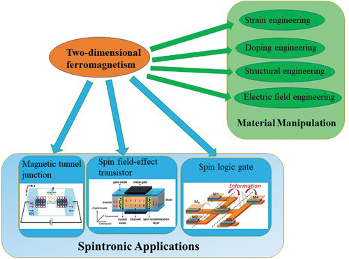
Since the first report on truly two-dimensional (2D) magnetic materials in 2017, a wide variety of merging 2D magnetic materials with unusual physical characteristics have been discovered and thus provide an effective platform for exploring the associated novel 2D spintronic devices, which have been made significant progress in both theoretical and experimental studies. Herein, we make a comprehensive review on the recent scientific endeavors and advances on the various engineering strategies on 2D ferromagnets, such as strain-, doping-, structural- and electric field-engineering, toward practical spintronic applications, including spin tunneling junctions, spin field-effect transistors and spin logic gate, etc. In the last, we discuss on current challenges and future opportunities in this field, which may provide useful guidelines for scientists who are exploring the fundamental physical properties and practical spintronic devices of low-dimensional magnets.
Graphical abstract
1. Introduction
Xu and Zhang et al. independently reported the ferromagnetic behavior in atomically thin layers of chromium germanium telluride (Cr2Ge2Te6) [1] and chromium triiodide (CrI3) [Citation2] in 2017, using a polar magneto-optical Kerr effect microscopy technique. Subsequently, a wide variety of emerging two-dimensional (2D) materials with intrinsic magnetic ground states of ferromagnetism (FM) or anti-ferromagnetism (AFM) down to atomic-layer thicknesses have been discovered and predicted [Citation3,Citation4], as summarized in , for listing the values of their transition temperatures and coercive fields. Two-dimensional ferromagnetism was discovered in 2D materials with stable long-range magnetic ordering, exhibiting the ferromagnetic behavior at magnetic ground state. In comparison to the conventional bulk magnetic materials, the magnetic anisotropy plays a vital role for the stable magnetic order in 2D magnets. This can break the limitation of the Mermin–Wagner theorem that long-range magnetic order could not be induced in low dimensional isotropic systems with continuous symmetry at finite temperatures [Citation5]. The magnetic exchange mechanisms in conventional 3D bulk magnets, including direct exchange interaction, superexchange interaction, Stoner-magnetism, and Ruderman–Kittel–Kasuya–Yosida (RKKY) mechanisms, can be found in various 2D magnets [Citation6,Citation7]. Also, some interesting exchange mechanisms, knows as super-spuerexchange, extended superexchange, and multi-intermediate double exchange, are newly discovered in 2D magnetic systems [Citation7]. Meanwhile, distinct from their bulk materials, 2D magnets have an interesting thickness-dependent magnetism. For example, VSe2 and CrI3 monolayers demonstrated a ferromagnetic behavior, while their bilayer counterparts show interlayer-antiferromagnetism at low temperature [Citation8,Citation9]. The special attributes of 2D magnetism as compared to their bulk counterparts are briefly summarized below: (1) they show strong quantum confinement [Citation10]; (2) they can be artificially integrated into heterostructure with arbitrary and flexible choices [Citation11,Citation12]; (3) their properties are thickness-dependent and highly anisotropic [Citation13,Citation14]; (4) they are the naturally perfect structure for magnetic and electronic tunneling effect [Citation15,Citation16], (5) they have large deformation and great endurance under external strain [Citation17,Citation18] and (6) they exhibit full tunability by external electric field, indicating a great potential for practical applications in voltage-controlled spintronic devices [Citation19,Citation20].
Table 1. The values of transition temperatures and coercive fields for emerging 2D magnetic materials
Spintronics, exploiting the spin-polarized electrons/holes as the information carrier, has quickly attracted a great deal of attention in the field of next-generation nanoelectronics. Compared to conventional nanoelectronics, a low energy consumption could enable the switching of the spin state with a much faster operation in spintronic devices. Therefore, spintronics has been developed into the most promising technology aiming to achieve information storage, transmission, and processing. 2D materials have drawn tremendous attention in spintronics due to their distinctive spin-dependent properties, such as the long spin relaxation lengths and times in graphene [Citation21,Citation22] and the stable spin-valley locking in transition metal dichalcogenides [Citation23,Citation24]. Moreover, the heterostructures by van der Waals engineering offer an unprecedented platform for effectively regulating interfacial magnetic order by magnetic proximity effect, which can break through the limitation of individual 2D magnet [Citation25]. However, several challenges remained to be solved in 2D spintronics. Firstly, most 2D magnetic materials used in spintronics have low Curie temperature (Tc) far below room temperature, as shown in . Secondly, precise spin-state detection and manipulation have not been achieved yet, which means the inability of spin-information transmission and impossibility for its spintronic applications. Moreover, the polarization efficiency of the spin injection and gating are urgently in need of improvement. Consequently, the currently reported magnetoresistance in 2D spin-transport devices are still very low, which cannot be used for the basic logic unit in very-large-scale integration (VLSI).
With the rapid development of 2D spintronics, it is urgent to review on the latest studies on current 2D magnetic materials and their applications. This review will focus on the recent scientific endeavors on the various engineering strategies on 2D ferromagnets, such as strain-, doping-, structural- and electric field-engineering, toward practical spintronic applications, including spin tunneling junctions, spin field-effect transistors, and spin logic gate, etc. We have chosen strain-, doping-, structural- and electric field-engineering as the highlighted subtopics because all of strategies are proven to be very effective approaches to tune the individual properties of atomic layers. Also, these engineering methods have been proficiently achieved in the experiments, such as substrate bending for strain-engineering [Citation26], ion liquid gating for doping-engineering [Citation27], pick-up transfer technique for integrating atomic hetero-structures [Citation28] and dual gate technique for electric-field engineering [Citation29] and so on. The various engineering approaches discussed in this review have induced multiple spintronic device-favored mechanisms, for example, the enhanced magnetic exchange interactions and elevated Curie temperature by strain-engineering, and the Stoner-ferromagnetism by electrostatic-doping, both of which are of great importance to the operational reliability of spintronic device at room temperature. Also, both the reduced spin relaxation and large carrier mobility induced by electrostatic-doing, and efficient spin-charge conversion and charge transport via proximity effect by structural engineering play a vital role in the performance of spin field-effect transistor. Meanwhile, the stronger spin filtering effect and enhanced magnetoresistance by using van der Waals heterostructure are also very favourable for the performance of magnetic tunnel junction and spin valve device. In the final section, we pointed out some current challenges and future opportunities in this field aiming to achieve practical applications. We attempt to summarize the underlying physical mechanism and issues for past various independently experimental and theoretical studies on the associated 2D magnetic nanostructures. We strongly believe that our comprehensive overview and general insight into 2D ferromagnetism can provide useful guidelines for exploring both novel engineering approaches and future candidates for spintronic devices of 2D magnets.
2. Manipulation of ferromagnetism in 2D materials
2.1. Strain engineering
The strain effect is inevitable in the experimental synthesis process for integrating 2D magnets on the substrate, for example, transferring CrI3 or Cr2Ge2Te6 atomic layers on SiO2/Si substrate by exfoliation [Citation1,Citation2], or fabrication of NbTe2 and VSe2 on SiO2/Si substrate by CVD/MBE [Citation30,Citation31]. The lattice mismatch between 2D magnets and the substrate can induce the interfacial strain, which can moderately modulate the performance of 2D magnets. Strain engineering has been demonstrated as a powerful technique for tuning the electronic properties of 2D materials, such as band gap, effective mass and carrier mobility (e.g. using substrate lattice mismatch [Citation32,Citation33] or substrate bending [Citation18]). Typically, in contrast to the bulk crystals, 2D materials demonstrate remarkable endurance under much larger strains [Citation17,Citation18]. For instance, single atomic layer FeSe and MoS2 can undergo external strains up to 6% and 11%, respectively [Citation34–36]. Also, the reduced dimension in 2D layered structure endows a smaller young modulus and softness. For example, it was reported that chromium trihalides are extremely soft with the small 2D Young’s modulus of 24, 29 and 34 N/m for monolayer CrI3, CrBr3 and CrCl3 by DFT calculations, respectively [Citation37]. The large strain endurance and soft nature of 2D layered structure imply that their magnetic properties can be effectively manipulated by strain engineering.
Strain can modulate the structural anisotropy, and consequently altering the magnetic anisotropy property by effectively tuning the magnetic exchange interactions. Webster et al. [Citation37] reported a theoretical study on the strain dependence of magnetic anisotropy energy in 2D monolayer chromium trihalides of CrCl3, CrBr3 and CrI3, respectively ()). They demonstrated that the magnetic anisotropic energy increases when a compressive strain is applied on CrI3 monolayer, while an opposite trend is observed in the other two compounds. In particular, the magnetic anisotropic energy of single layer CrI3 can be enhanced by 47% under a compressive strain of ε = 5%. Xu et al. demonstrated that, based on their first-principles calculations, an in-plane 90° rotation of the magnetic easy axis can be reversibly induced by applying the ferroelastic strain on chromium sulfifide halides CrSX (X = Cl, Br, I) monolayers [Citation38].
Figure 1. Change in energy with respect to the magnetization angle θM and MAE with respect to strain for (a) CrCl3, (b) CrBr3 and (c) CrI3. Reproduced with permission from [Citation37], Copyright 2018, American Physical Society. (d), MCD image of the CrI3 flake before (left) and after (right) applying a pressure of 1.8 GPa. (e) Magnetic field dependence of MCD at 3.5 K for two 2-layer (2 L) and two 5-layer (5 L) regions before (left) and after (right) applying pressure. Reproduced with permission from [Citation42], Copyright 2018, Nature.
![Figure 1. Change in energy with respect to the magnetization angle θM and MAE with respect to strain for (a) CrCl3, (b) CrBr3 and (c) CrI3. Reproduced with permission from [Citation37], Copyright 2018, American Physical Society. (d), MCD image of the CrI3 flake before (left) and after (right) applying a pressure of 1.8 GPa. (e) Magnetic field dependence of MCD at 3.5 K for two 2-layer (2 L) and two 5-layer (5 L) regions before (left) and after (right) applying pressure. Reproduced with permission from [Citation42], Copyright 2018, Nature.](/cms/asset/20e03cbb-b461-46e2-814f-a4d59e09a5f6/tsta_a_2030652_f0001_oc.jpg)
The lattice deformation induced by strain can alter the exchange coupling strength between magnetic ions, correspondingly change the magnetic thermal stability and the phase transition temperature. Zhou et al. [Citation39] showed NbS2 and NbSe2 monolayers can be magnetized with high Curie temperatures of 387 and 542 K under 10% biaxial tensile strain. This ferromagnetic character can be attributed to the competitive effects between through-space interaction and through-bond interaction. Miao et al. [Citation40] suggested that CrOCl monolayer could be feasibly prepared from their bulk counterparts because its exfoliation energy is only around 0.208 J/m2, which is only two-third of graphite. Moreover, the Tc of CrOCl monolayers can be significantly enhanced from 160 to 204 K under 5% biaxial tensile strain. Huang et al. [Citation41] predicted that room-temperature ferromagnetism could be achieved under a tensile in-plane strain of 4% in monolayer CrWI6 and CrWGe2Te6. The magnetic phase transition can also be induced by external strain, which can induce the multiple crystal-lattice effects, such as structural phase transition, layer-displacement, structural deformation and so on. Li et al. [Citation42] modulated the stacking order by a monoclinic-to-rhombohedral change via applying strong hydrostatic pressure on atomically thin CrI3 with 2D van der Waals structures. They observed an irreversible phase transition from interlayer AFM to FM in atomically thin CrI3 by magnetic circular dichroism microscopy (). Leon et al. [Citation43] demonstrated that a phase transition from AFM to FM in bilayer CrI3 can be induced by the in-plane compressive strain. They associated that behavior with the relative inter-layer displacement induced by external strain. Li et al. [Citation44] reported that the biaxial strain can induce a transition from FM to the AFM state in Mn-doped Silicene with the strain-tunable magnetic exchange couplings.
2.2. Doping
2.2.1. Magnetic doping
As an effective tool in functionalizing 2D systems, defect doping can induce magnetism in an atomic layered structure, where the long range magnetic order arises from the presence of single-atom defects in combination with an intrinsic discriminating mechanism in sublattices, in confirmation with Lieb’s theorem [Citation45,Citation46]. 2D transition-metal dichalcogenides (TMDs) provide the perfect platform with appropriate defective localization for using various doping approaches, including introducing vacancy, atomic substitution and displacement. The TMDs introduced by transition metal atoms (e.g. Fe, Co, Ni, Mn, etc.) with large magnetic moment have been proposed as diluted magnetic semiconductors, which may have promising applications in 2D spintronics [Citation47–55]. Mishra et al. [Citation50] reported a theoretical investigation on long-range FM ordering in Mn-doped MoS2, MoSe2, MoTe2 and WS2 by substituting Mo or W sites by Mn. Their first-principles calculations demonstrated an AFM exchange between the Mn d states and the p states of the chalcogen atoms, which can effectively regulate the long-range FM exchange of Mn atoms. Cheng et al. [Citation51] presented a comprehensive first-principles study of MoS2 monolayer doped by various transition metals. They observed ferromagnetism in MoS2 monolayer doped by Mn, Zn, Cd and Hg for concentration of 6.25%, while for Co and Fe dopants, AFM is observed due to Jahn-Teller distortions. Kanoun et al. [Citation52] investigated the electronic and magnetic properties of monolayer MoTe2 by introducing Mo vacancy or substituting Mo by various 3d transition metals by using first-principles calculations. They observed stable magnetic moment for all these cases, except for Ni defect. Zhao et al. [Citation53] observed ferromagnetism in 1 T-ZrSe2 monolayer by V, Cr, Mn, and Fe doping. They found that the magnetic moments of dopants have been significantly increased after including Hubbard potential Ueff during using density functional theory, indicating a transition from the low to high spin state. In addition to TMDs, diluted magnetic semiconductors have also been predicted by other 2D materials with magnetic dopants. Wu et al. [Citation54] theoretically demonstrated the room-temperature ferromagnetism with Curie temperature of 629 K in Fe-doped SnS2 with magnetic momentum of 2.0 μB per Fe atom. They observed the long-range ferromagnetism with intralayer sites occupied by the dopants, while it is paramagnetic with Fe fixed at interlayer sites. Zberecki et al. [Citation55] predicted the magnetism in TMs-doped 2D honeycomb structures of III–V binary compounds (i.e. GaN, AlN and InN). Another useful strategy for magnetic doping is through introducing atomic vacancies. Yazyev et al. [Citation56] demonstrated that, based on first-principles calculations, the itinerant magnetism can be induced in graphene with magnetic moments of 1 μB per hydrogen chemisorption defect and 1.12–1.53 μB per vacancy defect for various defect concentrations. The type of magnetism (i.e. FM or AFM) is determined by whether introducing truly disordered system during defect engineering. Jang et al. [Citation57] showed that Fe3GeTe2 is not FM but intrinsically has AFM ground state by using first-principles calculations. They also proposed that the hole doping induced by Fe deficiency can induce AFM to FM transition.
It is noteworthy that the theoretical studies mostly focused on constructing 2D magnetic lattice at the atomic-scale with enhanced magnetic moments, stronger exchange interactions and elevated Curie temperatures, while the experimental studies turned their attentions to spin transport properties, including confined spin relaxation, effective spin-charge conversion, large magnetoresistance, high carrier mobility and so on. Apparently, experimental concentrations on the spin transport properties in 2D systems are aiming to develop practical spintronic devices, such as spin field transistors and magnetic tunnel junction. Experimental studies on magnetic doping in 2D layered structures and van der Waals (vdW) heterostructures have been made great progress. Pi et al. [Citation58] reported the effects of surface gold deposition on spin transport in graphene by fabricating a spin valve device at low temperature. They showed that the charge impurity scattering plays a minor role in spin relaxation while a significant enhancement of spin lifetime from 50 to 150 ps was observed with increased gold coverage. Wang’s group [Citation59] experimentally demonstrated an effective regulation on magnetization via giant spin-orbit torque induced by an in-plane current in an epitaxial Cr-doped topological insulator film on GaAs substrates. The effective field to the in-plane current amplitude ratio and the spin Hall angle have been measured as several orders of magnitude larger than that in undoped heavy metal/ferromagnetic heterostructures ()). Furthermore, this team [Citation60] reported an effective electric field control of spin-orbit torque in a Cr-doped (Bi0.5Sb0.42)2Te3 thin film by using the spin field-effect transistor. The SOT intensity can be regulated by several orders of magnitude by varying the gate voltage with an effective magnetization switching. Nie et al. [Citation61] fabricated the unique MnxGe1-x nanomeshes with controllable Mn-doping density by nanosphere lithography. The superconducting quantum interference device demonstrated a high Tc above 400 K, which indicated a significant enhancement of magnetic exchange couplings as a result of quantum confinement effect in unique nanomeshed structure. Furthermore, a giant magnetoresistance of ~8,000% is realized at low temperature of 30 K in Mn0.03Ge0.97 nanomesh. Li et al. [Citation62] synthesized Fe-doped SnS2 bulk crystals with different Fe contents via a direct vapor-phase method, and then obtained their monolayer flakes via mechanical exfoliation. The electric transport measurement showed that the field-effect transistor based on exfoliated Fe0.021Sn0.979S2 demonstrate a high on-off ratio of ~1.2 × 10⁶ and carrier mobility of ~6.1 cm2 V−1 s−1. The magnetic measurements exhibited FM ground state with a remarkable perpendicular anisotropy at 2 K and a Curie temperature of ~31 K in Fe0.021Sn0.979S2 nanosheet. Tokmachev et al. [Citation63] fabricated layered silicene doped with rare-earth ions (Gd3+ and Eu2+) ranging from the bulk down to one monolayer. They demonstrated a thickness-dependent magnetism that the bulk is antiferromagnetic while its ultrathin layers have intrinsic 2D in-plane ferromagnetism.
Figure 2. (a) Schematic of the four stable magnetization states when passing a large d.c. current and applying an in-plane external magnetic field. The effective spin–orbit field induced by the d.c. current and the anisotropy field are both considered. (b) The AHE resistance as a function of the in-plane external magnetic field when passing a constant d.c. current at 1.9 K. (c) Current-induced magnetization switching in the Hall bar device at 1.9 K in the presence of a constant in-plane external magnetic field. (d) Phase diagram of the magnetization state in the presence of an in-plane external magnetic field By and a d.c. current. Reproduced with permission from [Citation59], Copyright 2014, Nature. (e) Conductance map [dI/dV(x,E)] along the dashed line in (f). (f) STM topography of a single H atom on graphene. (g) Comparison between DFT calculations for the local magnetic moment and the height of the occupied projected DOS (PDOS) peak. (h) Calculated magnetic moments induced by H chemisorption. Reproduced with permission from [Citation64], Copyright 2016, Science.
![Figure 2. (a) Schematic of the four stable magnetization states when passing a large d.c. current and applying an in-plane external magnetic field. The effective spin–orbit field induced by the d.c. current and the anisotropy field are both considered. (b) The AHE resistance as a function of the in-plane external magnetic field when passing a constant d.c. current at 1.9 K. (c) Current-induced magnetization switching in the Hall bar device at 1.9 K in the presence of a constant in-plane external magnetic field. (d) Phase diagram of the magnetization state in the presence of an in-plane external magnetic field By and a d.c. current. Reproduced with permission from [Citation59], Copyright 2014, Nature. (e) Conductance map [dI/dV(x,E)] along the dashed line in (f). (f) STM topography of a single H atom on graphene. (g) Comparison between DFT calculations for the local magnetic moment and the height of the occupied projected DOS (PDOS) peak. (h) Calculated magnetic moments induced by H chemisorption. Reproduced with permission from [Citation64], Copyright 2016, Science.](/cms/asset/be6c64f5-1418-40dc-86fd-e18235a74314/tsta_a_2030652_f0002_oc.jpg)
The stable long-range magnetic ordering and local magnetic moments can be also induced in non-magnetic 2D materials with non-magnetic dopants. Only one state of π-state couple near the Fermi level can be occupied by single electron due to the electrostatic Coulomb repulsion, which can extend the spatial range of the direct magnetic coupling by several nanometers. This can break the limitation of the localized magnetic coupling effect with relatively short spin exchange distance, which is the prerequisite of the conventional magnetic doping with metallic ions. González-Herrero et al. [Citation64] demonstrated that a spin polarization and stable magnetic ordering can be induced in hydrogen-adsorbed graphene by both scanning tunneling microscopy experiments and first-principles calculations. They observed that the magnetic moments are essentially localized between the carbon atoms in graphene-sublattice in an opposite direction with the chemisorbed-hydrogen locations (). They also demonstrated a remarkably precise control of magnetic momentum by selectively removing chemisorbed-hydrogen atoms in the arbitrary sublattice.
2.2.2. Electrostatic doping
In contrast to magnetic doping, electrostatic doping can also be used to control the carrier concentrations of the ferromagnets by virtue of without introducing defects. In comparison to 3D bulk materials, atomic thin 2D materials take great advantage of naturally large surface-area-to-volume ratio for charge doping engineering. By virtue of their atomic thickness, the gating technology can tune the carrier doping concentrations up to 1013 cm−2 in MoS2 and WSe2 monolayer [Citation29,Citation65] and 1014 cm−2 in 2D Fe3GeTe2 thin film [Citation66], and up to the order of 1014 cm−2 in graphene [Citation26,Citation27]. Hence, gate-tunable doping has become an effective way to modulate the electronic state around the Fermi energy.
Błonski et al. [Citation67] reported the stable ferromagnetism can be induced in graphene by doping with graphitic, pyridinic, and chemisorbed nitrogen. Graphene doped below 5 at.% of nitrogen shows dominant diamagnetic; while if the doping concentration is above 5 at.%, it demonstrated a transition to ferromagnetism with Tc of 69 K. Their first-principles calculations showed that graphitic nitrogen atoms play the predominant role in inducing Stoner-magnetism, indicating a spin-polarized electrons near Fermi levels. Zhang et al. [Citation68] showed that electrostatic doping can endow single layer PdSe2 with half metal Stoner-ferromagnetism and high Tc above room temperature. Yu et al. [Citation69] and Wang et al. [Citation70] independently predicted that the hole doping can cause half-metallicity and nearly 100% spin-polarization in monolayer CrI3 by using first-principles calculations. Meanwhile, the magnetoresistance can reach over 106% via hole doping ()). Moreover, the stability of itinerant ferromagnetism can be significantly strengthened by hole doping so that a room temperature of Tc can be achieved with the doping concentration of 8.49 × 1014 cm−2 ()).
Figure 3. (a) The device model based on the hole-doped 1 L-CrI3. (b) The magnetoresistance vs. the bias voltage. The hole doping density is 0.05 e/atom (9.43 × 1013 cm−2). (c) The magnetic moment as a function of temperature under various hole doping density. Reproduced with permission from [Citation69], Copyright 2021, Elsevier. (d) The crystal structure of monolayer GaSe. (e) Carrier density dependence of spin magnetic moment per carrier and spin-polarization energy per carrier in the out-of-plane spin-polarized ferromagnetic state. (f) Band structures along high symmetry directions at carrier density of 7 × 10¹³/cm2. Reproduced with permission from [Citation45], Copyright 2015, American Physical Society.
![Figure 3. (a) The device model based on the hole-doped 1 L-CrI3. (b) The magnetoresistance vs. the bias voltage. The hole doping density is 0.05 e/atom (9.43 × 1013 cm−2). (c) The magnetic moment as a function of temperature under various hole doping density. Reproduced with permission from [Citation69], Copyright 2021, Elsevier. (d) The crystal structure of monolayer GaSe. (e) Carrier density dependence of spin magnetic moment per carrier and spin-polarization energy per carrier in the out-of-plane spin-polarized ferromagnetic state. (f) Band structures along high symmetry directions at carrier density of 7 × 10¹³/cm2. Reproduced with permission from [Citation45], Copyright 2015, American Physical Society.](/cms/asset/6d06d267-ec3b-4aa7-a962-9eb7c419e607/tsta_a_2030652_f0003_oc.jpg)
The electrostatic gating on non-magnetic 2D materials could also induce the large electronic density of states near the Fermi level with a strong spin-exchange, resulting in spontaneous spin polarization and the stable itinerant ferromagnetism. Cao et al. [Citation71] and Wu et al. [Citation72] separately predicted that hole doping can induce itinerant ferromagnetism and half-metallicity in single layer GaSe. The doping system exhibits nearly constant magnetic moment per carrier around 1.0 µB with the doping concentration between 3 × 10¹³/cm2 and 1 × 10¹⁴/cm2. The itinerant ferromagnetism is attributable to the large exchange splitting between spin-up and spin-down electrons at top of valence band and the high electronic density of states with a remarkable van Hove singularity near Fermi level [Citation45] (). The family of group IIIA metal-monochalcogenide MX (M = Ga, In; X = S, Se, Te) single layers [Citation73] and 2D holey C2N crystals [Citation74] have also been demonstrated to possess high density of states at band edges, leading to Stoner-ferromagnetism via carrier doping engineering. Fu et al. [Citation75] predicted that in buckled phosphorene and arsenene, hole doping can induce Stoner-ferromagnetim with a plateau magnetic moment per carrier around 1.0 µB in a broad range of doping concentrations between 3 × 10¹³/cm2 and 5.6 × 10¹⁴/cm2. They also demonstrated the strain-tunable Stoner-ferromagnetism by altering the band orders at top of valence band.
2.3. Structural engineering
Most of spin logic devices, including spin field-effect transistor, spin valve and magnetic memory, require a high on-off ratio, which means a great distinction in spin transport properties between spin-up and spin-down electrons. However, this is a challenge for graphene and even for most 2D insulators [Citation76,Citation77]. One approach to overcome this obstacle is to interface 2D materials with 3D magnets (i.e. exfoliation). In comparison to this approach by using 3D magnets, a 2D van der Waals heterostructure has the following advantages: (i) The interlayer twisting angle and the various stacking orders endow the heterostructure with richer properties by the arbitrary choice of direct- or indirect-bandgap, which can broaden the applicability for high-performing magnetic devices [Citation78]. (ii) There is no request for the lattice matching, accordingly keeping their pristine atomic layered structure without chemical bonding and interfacial damage [Citation12]. (iii) The diverse and flexible choices of 2D magnetic materials can enable the precise control of the fabrication process and comprehensive characterization of the heterostructure [Citation11]. (iv) The proximity coupling effect at atomically sharp interfaces between vdW materials and magnetic substrates could effectively tune the spin-related properties in pristine layer, including spin-orbit coupling, spin polarization and spin transport [Citation79]. (v) The heterostructure can modulate the magnetic ions in 2D diluted magnetic semiconductors, and consequently raising the temperature at which the quantum anomalous hall effect (QAHE) can be observed [Citation80]. (vi) Multiple interfacial mechanisms, including charge transfer, band alignment, symmetry breaking, orbital hybridization and layer polarizability, have been proposed as very effective tools to modulate the magnetic properties [Citation81].
The 2D heterostucture based on 2D non-magnetic material/magnets can have promising valleytronic applications. Valleytronics is a novel practical approach for information processing and storage by utilizing the spin and valley degrees of electron freedom. The 2D heterostructure can lift the valley degeneracy and produce the valley splitting by interfacial effect and ultimately induce a robust and nonvolatile valley polarization, which is of great importance to the creation, conduction and storage of magnetic informations. Sabirianov et al. [Citation82] fabricated the heterostructure of WS2 monolayer and ferromagnet EuS. They found that the giant valley splitting of 16 meV can be induced by magnetic proximity effect, which is two orders of magnitude larger than that obtained by applying external magnetic field. Their first-principles calculations revealed that the sign reversal between WSe2/EuS and WS2/EuS is attributed to the different atomic termination at EuS surface sites. Kang et al. [Citation83] performed first-principles calculations and observed a considerable valley splitting energy of 376 meV at the valance band of 2D WS2/h-VN heterostructure, which corresponds to an effective Zeeman magnetic field of 2703 T. Feng et al. [Citation84] also used first-principles calculations to demonstrate a large valley spitting of 214 meV at the valence band of monolayer WS2 on the MnO(111) surface, which is equivalent to a Zeeman magnetic field of 1516 T. Gong et al. [Citation85] observed a large valley splitting over 30 meV at the conduction band of WSe2 monolayer in 2D MnPSe3/WSe2 heterostructure.
Additionally, structural engineering can also endow the significant enhancement of magnetic anisotropy, exchange interactions and Curie temperature as a result of interfacial effect. Yamasaki et al. [Citation86] fabricated the vdW heterostructure composed of Cr1/3TaS2 and ferromagnet Fe1/4TaS2 with a native T2O5 tunnel barrier in between by employing a dry-transfer method. Cr1/3TaS2 exhibited a great in-plane magnetic anisotropy and a maximum tunnel magnetoresistance (TMR) of 13% versus bias voltage. Hou et al. [Citation87] showed that a thickness-dependent spin splitting of the Dirac cone at Bi2Se3 films surface can be realized via forming the topologically nontrivial CrI3/Bi2Se3/CrI3 heterostructure by their first-principles calculations. Dong et al. [Citation88] showed that the magnetic anisotropic energy of Cr2Ge2Te6/PtSe2 bilayer heterostructure can be enhanced by 70% compared with single layer Cr2Ge2Te6 by using first-principles calculations. They attributed this great enhancement to both the presence of Dzyaloshinskii–Moriya interaction and single ion anisotropy. Additionally, the Curie temperature is also increased significantly above 600 K by DFT calculations.
Structural engineering can also effectively improve the spin transport of 2D magnets, via enhancing spin injection, polarization and magnetoresistance as well as introducing multiple magnetoresistance states, all of which are aiming towards the practical goals of spin valve, spin field-effect transistor, magnetic tunnel junction and so on. Gurram et al. [Citation89] experimentally reported that graphene can have a giant spin-injection efficiency and large spin polarization under bias voltage in bilayer h-BN/graphene/h-BN heterostructure by using four-terminal structure with ferromagnetic electrodes. Ghazaryan et al. [Citation90] studied tunneling effect in graphene/CrBr3/graphene, where thin ferromagnetic CrBr3 are tunneling barriers and graphene are used as electrodes. They demonstrated that the spin injection and spin polarization through thin ferromagnet CrBr3 barriers are mainly associated with the momentum conservation condition, which is manipulated by magnon emission at low temperature (). Albarakati et al. [Citation91] demonstrated unusual antisymmetric magnetoresistance effect in vdW Fe3GeTe2/graphite/Fe3GeTe2 heterostructure devices. When the magnetic momentum in two Fe3GeTe2 flakes are antiparallel, the magnetoresistance of these devices possesses distinct high- or low-resistance states, while it adopts an intermediate state in case of parallel magnetization in these two ferromagnets. Based on their first-principles calculations, the three-resistance characteristic was attributable to spin momentum locking at the graphite/FGT interface as a result of Rashba-split in 2D electron gas. Hu et al. [Citation92] theoretically studied the spin transport property in a vdW heterostructure of MnPS3/Fe3GeTe2, where MnPS3 is an intrinsic antiferromagnet while Fe3GeTe2 is a ferromagnet. The magnetoresistance exhibits three spin-transport states of high-, intermediate- and lowlevels. This phenomenon is attributed to a desynchronized phase during magnetic switching at MnPS3/Fe3GeTe2 interface under external magnetic field (). Lin et al. [Citation93] investigated the spin transport property of the spin-valve device based on Fe3GeTe2/MoS2/Fe3GeTe2 vdW heterostructures. The current–voltage curve illustrates a perfect linear characteristic, indicating a good Ohmic contact at Fe3GeTe2 /MoS2 interfaces. The magnitude of the magnetoresistance is measured as 3.1% at 10 K and it decreases monotonically as the increasing temperature up to 200 K. Khan et al. [Citation94] reported on the spin transport properties of the spin valve heterostructure interfacing by bilayer graphene and single-layer MoSe2 with metallic cobalt and nickel–iron alloy as the ferromagnetic electrodes. The device exhibited a positive MR, i.e. ~ 1.71% and ~ 1.86% at low temperature before and after annealing, respectively.
Figure 4. (a) An optical micrograph of the investigated device. (b) Differential tunneling conductance G as a function of B‖ and Vb (Vg = 0 V). The color scale is blue to white to red, 6 nS to 12 nS to 19 nS. (c) Bias position of the step-like features in G as a function of B‖. (d) Calculated magnon density of states for T = 10 K, B = 0 T (blue line), T = 10 K, B = 6.25 T (black line), and T = Tc, B = 0 T (red line). The same calculations provide Tc = 88 K. (e) Calculated changes of the position of the van Hove singularities in magnon density of states. Reproduced with permission from [Citation90], Copyright 2018, Nature. (d) as a function of magnetic field for temperatures close to Tc. (f) Schematic illustration and optical image of the vdW heterostructure of MPS/FGT. (g) Magnetic field dependence of Rxx and Rxy in the MPS/FGT heterostructure at 10 K with a positive shift of HEB = 160 Oe at a cooling field of HFC = −10 kOe. (h) Schematic diagram of the spin polarization and magnetization at interface and bulk FGT. Reproduced with permission from [Citation92], Copyright 2020, American Chemical Society.
![Figure 4. (a) An optical micrograph of the investigated device. (b) Differential tunneling conductance G as a function of B‖ and Vb (Vg = 0 V). The color scale is blue to white to red, 6 nS to 12 nS to 19 nS. (c) Bias position of the step-like features in G as a function of B‖. (d) Calculated magnon density of states for T = 10 K, B = 0 T (blue line), T = 10 K, B = 6.25 T (black line), and T = Tc, B = 0 T (red line). The same calculations provide Tc = 88 K. (e) Calculated changes of the position of the van Hove singularities in magnon density of states. Reproduced with permission from [Citation90], Copyright 2018, Nature. (d) as a function of magnetic field for temperatures close to Tc. (f) Schematic illustration and optical image of the vdW heterostructure of MPS/FGT. (g) Magnetic field dependence of Rxx and Rxy in the MPS/FGT heterostructure at 10 K with a positive shift of HEB = 160 Oe at a cooling field of HFC = −10 kOe. (h) Schematic diagram of the spin polarization and magnetization at interface and bulk FGT. Reproduced with permission from [Citation92], Copyright 2020, American Chemical Society.](/cms/asset/3bd38934-d46b-4c7c-9548-58f44c28cfbe/tsta_a_2030652_f0004_oc.jpg)
With the fast development of synthesis technology for 2D heterostructures, proximity effect could be employed to effectively modulate the multiple characteristics of pristine layer. A given 2D material can be endowed with superconducting, magnetic, or topologically states by proximity effect. For instance, although pristine graphene has negligible SOC strength, it can realize efficient spin-charge conversion and charge transport via proximity effect with the adjacent ferromagnets [Citation95–97]. Mendes et al. [Citation95] fabricated graphene on top of thin ferromagnetic insulator yttrium iron garnet (YIG) film by large-area CVD method. They observed that the spin current can be converted into charge current by the inverse Edelstein effect.
Graphene can also gain magnetism and spin transport by magnetic proximity effect [Citation98,Citation99]. Wang et al. [Citation99] demonstrated the anomalous Hall effect with Hall conductance of ~2e2/h at low temperature of 2 K in graphene when adhering to atomically thin YIG ferromagnet. Their observed the long-range ferromagnetic order induced by proximity effect in graphene/YIG heterostructure. The significant enhancement of spin-orbit coupling strength in comparison to the pristine graphene has been also demonstrated. Yang et al. [Citation100] found that, based on their first-principles calculations, the spin-polarization ratio of pz orbitals in graphene is about 24%, together with a large spin exchange-splitting energy of about 36 meV due to C-pz and Eu-4 f interaction in graphene/EuO heterostructure. Meanwhile, they demonstrated that the stacking order and interlayer distance of the hetero-atomic layers mainly determined the position of the Dirac cone ()). Wei et al. [Citation101] reported a substantial enhancement of the spin signal by several orders of magnitude stemming from the Zeeman spin Hall effect in graphene induced by adjacent ferromagnetic insulator (EuS). They also demonstrated that the strong exchange magnetic field can lift the ferromagnetic ground-states degeneracy of Dirac electrons and create the spin-polarized valley-singlet state (). Lazić et al. [Citation102] showed that the magnetic proximity tuned by gating effect can occur in 2D heterostructures, i.e. Co/bilayer graphene, Co/BN/graphene, and Co/BN/benzene, due to the vdW bonding interaction. They pointed out that the van der Waals bonding is required for both modulating the spin polarization and enabling its sign reversal. Zhong et al. [Citation103] demonstrated an effective regulation of the valley dynamics in WSe2 via switching the CrI3 magnetization in CrI3/WSe2 heterostructure. Their photoluminescence measurement at low temperature reveals zero-field valley splitting of ~3.5 meV, which is equivalent to an effective 13 T magnetic field due to the presence of ferromagnetic substrate CrI3. Wu et al. [Citation104] found that the magnetic proximity effect can result in a remarkable Zeeman splitting equivalent to the presence of magnetic field with magnitudes of several hundreds of tesla in graphene adhering to ferromagnetic EuO substrate. They also demonstrated a magnetic state transition of the first Landau level from ferromagnetism to a canted antiferromagnetism via applying the perpendicular magnetic field. Tong et al. [Citation105] theoretically studied the magnetic proximity effect in vdW moire´ superlattice formed by semiconductor monolayer BAs and ferromagnetic monolayer CrI3 by first-principles calculations. Their study showed that the interlayer atomic configuration plays a very important role in the magnetic proximity effect due to the spin-dependent interlayer hopping. Karpiak et al. [Citation106] observed that the spin transport and precession in graphene can be effectively modulated by adjacent ferromagnetic Cr2Ge2Te6 with strong anisotropy via magnetic proximity effect. The lifetime for perpendicular spins is measured as 3.9 times larger than that of the in-plane counterpart, indicating the strong anisotropy of spin texture spectroscopy in graphene. Recently, Zhang et al. [Citation107] showed that the ferromagnetism of Fe3GeTe2 thin films can be modulated by interfacing with atomically thin FePS3. The Curie temperature of Fe3GeTe2 is improved by 30 K in FePS3/Fe3GeTe2 and 35 K in FePS3/Fe3GeTe2/FePS3 in comparison to the pristine Fe3GeTe2. Meanwhile, the coercive field is doubled due to the proximity coupling effect.
Figure 5. (a) Side view and (b) six sublattices of the calculated crystalline structures for graphene on top of a six bilayer EuO film. (c) Total density of states of pz orbitals of graphene. (d) Band structures for graphene on EuO with graphene shifted by different distances. Reproduced with permission from [Citation100], Copyright 2013, American Physical Society. (e) Top panel: a false-colored device image taken by a scanning electron microscope. Bottom panel: a schematic drawing of the Zeeman splitting of the Dirac cone in graphene and the spin-up hole-like and spin-down electron-like carriers at the charge neutrality point. (f) Top panel: Non-local resistance Rnl as a function of gate voltage Vg under dierent µ0H for a CVD-graphene/EuS device at temperature T. Bottom panel: Comparison of Rnl,D versus µ0H curves for the graphene device before (pristine) and after EuS deposition. (g) Top panel: Comparison of the temperature dependence of Rnl,D and of M of the graphene/EuS heterostructure. Bottom panel: Comparison of the normalized non-local resistance and longitudinal resistance in graphene/EuS. (h) Top panel: Field dependence of Rnl,D in graphene/EuS versus that in graphene/AlOx. Bottom panel: Quantitative estimation of the Zeeman splitting energy Ez in the presence of EuS. Reproduced with permission from [Citation101], Copyright 2016, Nature.
![Figure 5. (a) Side view and (b) six sublattices of the calculated crystalline structures for graphene on top of a six bilayer EuO film. (c) Total density of states of pz orbitals of graphene. (d) Band structures for graphene on EuO with graphene shifted by different distances. Reproduced with permission from [Citation100], Copyright 2013, American Physical Society. (e) Top panel: a false-colored device image taken by a scanning electron microscope. Bottom panel: a schematic drawing of the Zeeman splitting of the Dirac cone in graphene and the spin-up hole-like and spin-down electron-like carriers at the charge neutrality point. (f) Top panel: Non-local resistance Rnl as a function of gate voltage Vg under dierent µ0H for a CVD-graphene/EuS device at temperature T. Bottom panel: Comparison of Rnl,D versus µ0H curves for the graphene device before (pristine) and after EuS deposition. (g) Top panel: Comparison of the temperature dependence of Rnl,D and of M of the graphene/EuS heterostructure. Bottom panel: Comparison of the normalized non-local resistance and longitudinal resistance in graphene/EuS. (h) Top panel: Field dependence of Rnl,D in graphene/EuS versus that in graphene/AlOx. Bottom panel: Quantitative estimation of the Zeeman splitting energy Ez in the presence of EuS. Reproduced with permission from [Citation101], Copyright 2016, Nature.](/cms/asset/b42de9a2-eb63-4501-ab1f-1dbec5a7cc5b/tsta_a_2030652_f0005_oc.jpg)
The quantum anomalous Hall effect (QAHE) can be made in topological insulator thin films by magnetic doping to introduce spontaneous magnetizations, such as Cr and V doped Bi2Te3 [Citation108]. Also, spin-gapless semiconductors (SGSs) with intrinsic 2D magnetism are of great importance to the realization of topological Chern phases [Citation3,Citation109]. Ferromagnetic SGSs have several obvious advantages over magnetic doping in topological insulator for realizing QAHE. First, due to the experimental challenge in the uniform distribution of the magnetic impurities, the temperature at which QAHE can be realized is extremely low. Also, the ferromagnetic ground state can be sustainable against the thermal fluctuations at high temperature by a comprehensive and suitable search for SGSs. On the other hand, the Curie temperature in the diluted magnetic semiconductors can not be effectively raised without breaking the band topology. In ferromagnetic SGS the transition metal ions typically form honeycomb lattice structure including monolayers of transition-metal trihalides such as RuI3 [Citation110], MnBr3 [Citation111] and NiCl3 [Citation112], or transition-metal oxides V2O3 [Citation113] and Nb2O3 [Citation114]. Kagome lattice structure is also prototypically suitable for ferromagnetic SGSs, including single layer Co3Sn2S2 [Citation115], Fe3Sn2 [Citation116], CoSn [Citation117] and so on.
Beyond conventional spintronics, the integration of magnetic materials with topological insulators has led to the genesis of topological spintronics [Citation118]. Hybrid structures that interface topological surface states with magnetism show promising spintronic device-related phenomena such as extremely efficient charge-to-spin conversion beyond the dissipationless charge transport from topologically protected edge states [Citation119]. Several important observations in topological spintronics, including large spin-orbit torque, geometric Hall effect, topological antiferromagnetism and topological magnetoelectric effect, have provided great scientific opportunities toward practical goals of spintronic devices [Citation120]. Axion insulator differs from the quantum anomalous Hall insulator in that the former is capable of the topological (near-quantized) magnetoelectric effect with broken time reversal symmetry but preserving spatial inversion symmetry [Citation121]. To produce the axion insulating phase, an antiparallel magnetization and an opposite sign of the exchange gap should be realized on the top and bottom surfaces. Axion insulating state is prototypically characterized by a zero Hall plateau with zero Hall conductance [Citation122]. A moderate magnetic field can drive a quantum phase transition from axion insulating phase to Chern insulator phase with zero longitudinal conductance and quantized Hall conductance [Citation123].
2.4. Electric field engineering
The effective manipulation of a spin state via applying electric field plays a very important role in functionalizing 2D magnetic devices. The effective regulation of magnetism via external electric fields boosts the development of electrically controlled spintronic devices, such as voltage-controlled magnonic logic device and spin field-effect transistors with fast operation and low power consumption. However, the precise modulation of the electronic spins and the magnetism in 2D materials by external electric field has been challenging.
Multiple efforts have been devoted to the electric-field control of magnetism in 2D monolayers. Deng et al. [Citation66] showed that, via ionic gating, the induced extreme charge carriers can strengthen the itinerant ferromagnetism and dramatically elevates Tc of single-layer Fe3GeTe2 above room temperature. The gate voltage can also significantly modulate the coercive field. The ferromagnetic transition temperature Tc was extracted in virtue of anomalous Hall effect measurement (). Wang et al. [Citation124] showed that, via using ionic liquid and solid Si gating technology, the bipolar field effect transistor based on ferromagnetic insulating Cr2Ge2Te6 thin film exhibited a doping-dependent magnetism. The magneto-optical Kerr measurements demonstrated the significantly reduced saturation field and larger magnetic moment with the elevated gate voltage below the Curie temperature. Liu et al. [Citation125] observed that the Neel-type magnetic Skyrmion spin configurations become energetic-favorable than ferromagnetic spin states as a result of applying out-of-plane electric field by breaking the inversion symmetry and inducing nontrivial Dzyaloshinskii–Moriya interaction.
Figure 6. (a) Conductance as a function of gate voltage Vg measured in a trilayer FGT device. Data were obtained at T = 330 K. (b, c) Rxy as a function of external magnetic field recorded at representative gate voltages, obtained at T = 10 K (b) and T = 240 K (c). (d) Phase diagram of the trilayer FGT sample as the gate voltage and temperature are varied. (e) Coercive field as a function of the gate voltage. (f) Rxy of a four-layer FGT flake under a gate voltage of Vg = 2.1 V. (g) Remanent Hall resistance Rxy as a function of temperature. Reproduced with permission from [Citation66], Copyright 2018, Nature. (h) A schematic side view of a dual-gate bilayer CrI3 field-effect device. (i) Doping density–magnetic field phase diagram at 4 K. (j) MCD versus magnetic field at 4 K at representative gate voltages. Reproduced with permission from [Citation127], Copyright 2018, Nature.
![Figure 6. (a) Conductance as a function of gate voltage Vg measured in a trilayer FGT device. Data were obtained at T = 330 K. (b, c) Rxy as a function of external magnetic field recorded at representative gate voltages, obtained at T = 10 K (b) and T = 240 K (c). (d) Phase diagram of the trilayer FGT sample as the gate voltage and temperature are varied. (e) Coercive field as a function of the gate voltage. (f) Rxy of a four-layer FGT flake under a gate voltage of Vg = 2.1 V. (g) Remanent Hall resistance Rxy as a function of temperature. Reproduced with permission from [Citation66], Copyright 2018, Nature. (h) A schematic side view of a dual-gate bilayer CrI3 field-effect device. (i) Doping density–magnetic field phase diagram at 4 K. (j) MCD versus magnetic field at 4 K at representative gate voltages. Reproduced with permission from [Citation127], Copyright 2018, Nature.](/cms/asset/aaa96de0-a1ef-4c5f-9ca3-facb6d1119d8/tsta_a_2030652_f0006_oc.jpg)
Additionally, the electric-field control of interlayer magnetism in 2D layered structure have been widely reported with regard to three aspects. First, the multiple magnetic states can be induced by external electric field as a result of different patterns of layer magnetizations without breaking the magnetism of individual layer. Second, the electric field can switch the interlayer spin states and reconfigure the spin filters, indicating a great potential for magnetic logic gate device. Lastly, electric field can also induce some novel magnetic configurations, such as Skyrmion ferromagnetism in CrI3 [Citation125] and spiral ferromagnetism in twisted bilayer graphene [Citation126]. Mak et al. [Citation127] demonstrated electrostatic doping effect on the magnetic properties of bilayer CrI3 by using graphene/CrI3 vertical heterostructure. Doping can significantly modify the interlayer exchange coupling, coercive field and Tc, showing that electron/hole doping can weaken/strengthen the long-range magnetic order. The antiferromagnetic phase monotonically diminished with increasing electron doping concentration and then, totally vanished and turned into ferromagnetic phase after the elevated electron doping reaches ~2.5 × 1013 cm−2 (). Mak et al. [Citation128] also demonstrated an effective regulation of magnetism via applying transverse electrical field in bilayer antiferromagnetic CrI3. They observed that the external electric field can induce a linear magnetoelectric effect as a result of interlayer potential difference. Xu et al. [Citation129] used magneto-optical Kerr effect microscopy to study the electrostatic gate effect on the magnetism in CrI3 bilayers. They obtained electrical switching between ferromagnetic and antiferromagnetic states by applying magnetic fields near the metamagnetic transition. They also demonstrated that, due to the strong spin-layer locking, the linear gate-dependent Kerr effect signals with opposite slopes could occur with a time-reversal pair of layered antiferromagnetic states without external magnetic field. Xu et al. [Citation130] reported the electrical switching of multiple magnetic states in four-layer CrI3 sandwiched between two bipolar graphene electrodes in a dual-gated field effect device. They also observed an effective gate-modulation on TMR from 17,000% to 57,000%, which is tentatively attributed to the combination of magnetic proximity effect at graphene/CrI3 interface and electrical field modulation on the spin-dependent tunneling as a result of Fermi level shift. San-Jose et al. [Citation126] proposed that the relative lattice orientation between adjacent graphene layers can modulate the magnetic phases in twisted graphene bilayers. It shows a magnetic transition from lattice AFM phase to spiral FM phase for twisting graphene bilayers from 0° to a relative 120° misalignment. The vertical electric field can effectively switch the spiral FM phase and the lattice AFM phase with a relative 120° misalignment as a result of electrically tuned exchange coupling between adjacent graphene layers.
Electric field can also effectively improve the spin transport of 2D magnets via reducing spin relaxation and enhancing magnetoresistance, exhibiting a substantial potential for the practical application of spin valve device. Avsar et al. [Citation131] fabricated a semiconducting spin valve device by encapsulating ultrathin black phosphorus (~5 nm) into hexagonal boron nitride atomic layers. They observed a long spin relaxation time of ~4 ns with spin relaxation length of ~6 µm by measuring Hanle spin precession. Liang et al. [Citation132] showed the gate-tunable electrical spin-valve device with magnetoresistance of 1.1% in a multilayer MoS2 semiconducting channel on a ferromagnetic Co/MgO electrode by using a two-terminal configuration. They found that the spin relaxation is largely prevented with an enhanced spin diffusion length of 235 nm. Yang et al. [Citation133] theoretically investigated the spin transport in spin-valve device based on Fe3GeTe2 monolayer where a high magnetoresistance of ~390% was obtained and can be significantly increased to ~510% under the electric gates.
3 Spintronic applications
In recent years, 2D spintronics, which utilizes the spins of polarized electrons in 2D materials for information generation, transmission and storage, has attracted a great deal of attention, and may have plenty of promising applications beyond conventional complementary metal-oxide semiconductor electronics. Especially, the manipulation of the 2D magnetism by applying external electric field and carrier doping has drawn great attention for power-saving spintronics devices. With carrier-mediated magnetism, 2D ferromagnetic/antiferromagnetic semiconductors can develop into a suit of electrically controlled spintronic devices with non-volatility and rapid-operation, such as magnetic tunnel junction, spin field-effect transistor and spin logic gate.
3.1. 2D magnetic tunnel junction
The 2D magnetic tunnel junction (MTJ) is composed of two separate ferromagnets as electrodes and an intermediate insulating atomic layer. Tunnel magnetoresistance is a that occurs in a MTJ via applying bias voltage. The tunneling probability depends on the electronic density of states near the Fermi energy in the ferromagnets and the thickness of the insulating barrier. When the magnetizations in two ferromagnetic electrodes are parallel, their similar distributions of the electronic density of states near the Fermi level provide more tunneling opportunities, leading to a high conductance. On the other hand, when the magnetizations of two ferromagnets are antiparallel, a mismatch of their density of states will impede the tunneling with a low conductance.
Karpan et al. first reported a theoretical exploration on a MTJ based on Ni/Graphene/Co and Co/Graphene/Co by using graphene as tunneling barrier in 2007 [Citation134]. They proposed a strong interaction between graphene and nickel slab, opening a band gap in pz band of graphene at K point in Brillouin zone for antiparallel-spin configuration. This results in a large spin polarization close to 100% and an extremely large TMR has been achieved (). However, the subsequently experimental observations exhibit very low TMR in 2D MTJs based on graphene layered structure, holding the highest record TMR up to 31% [Citation118,Citation135–138]. Scientists have devoted further effort on some other 2D materials, such as semiconducting MoS2 and insulating hexagonal boron nitride (h-BN), to be employed as tunnel barrier layers [Citation139–141]. Piquemal-Banci et al. [Citation139] fabricated Fe/h-BN/Co MTJ by using the chemical vapor deposition (CVD) method. They demonstrated that the tunneling resistance was exponentially proportional to the number of layers in h-BN. They also observed a TMR of 6% for single layer h-BN as the tunnel barrier. Zhang et al. [Citation140] investigated Ni/MoS2/Ni and Co/MoS2/Co MTJs by their first-principles calculations, where larger TMR can be acquired by using Co as the ferromagnetic electrodes, with a maximum value of 63.86% for using five-layer MoS2 as the tunnel barrier and a negative value of −70.85% for single layer MoS2 structure.
Figure 7. (a) Conductances (▽),
(Δ) and
(×) of a Ni/Grn/Ni junction as a function of the number of graphene layers n for ideal junctions. (b) Majority and minority spin band structures (green) of a single graphene layer absorbed upon a 13 layer (111) Ni slab for a BC configuration with d = 3.3 Å, and an AC configuration with d = 2.0 Å. Reproduced with permission from [Citation134], Copyright 2007, American Physical Society. (c) Magnetic states of bilayer CrI3 with different external magnetic fields. (d) Schematic illustration of a 2D spin-filter MTJ with bilayer CrI3 sandwiched between graphene contact. (e) Tunneling current of a bilayer CrI3 sf-MTJ at selected magnetic fields. Reproduced with permission from [Citation142], Copyright 2018, Science.
![Figure 7. (a) Conductances GPmin (▽), GPmaj (Δ) and GAPσ (×) of a Ni/Grn/Ni junction as a function of the number of graphene layers n for ideal junctions. (b) Majority and minority spin band structures (green) of a single graphene layer absorbed upon a 13 layer (111) Ni slab for a BC configuration with d = 3.3 Å, and an AC configuration with d = 2.0 Å. Reproduced with permission from [Citation134], Copyright 2007, American Physical Society. (c) Magnetic states of bilayer CrI3 with different external magnetic fields. (d) Schematic illustration of a 2D spin-filter MTJ with bilayer CrI3 sandwiched between graphene contact. (e) Tunneling current of a bilayer CrI3 sf-MTJ at selected magnetic fields. Reproduced with permission from [Citation142], Copyright 2018, Science.](/cms/asset/40fec250-8fee-4485-86f2-66e3bf1e2345/tsta_a_2030652_f0007_oc.jpg)
Emerging 2D magnetic materials provide new choices and exhibit many surprising properties. Xu et al. [Citation142] fabricated multiple spin MTJs composed of graphene/CrI3/graphene vdW heterostructures. They demonstrated a significantly enhanced tunneling magnetoresistance with increasing number of CrI3 layers. A giant TMR of 19,000% for using four-layer CrI3 as the tunneling barrier at low temperatures was observed (), which is significantly larger than other MTJs with conventional tunneling materials (e.g. MgO [Citation143,Citation144]). Yang et al. [Citation145] reported the theoretical study on the spin transport properties of a MTJ based on MoSe2/VSe2/WSe2/VSe2/MoSe2 heterostructure by using non-equilibrium Green’s function method. Their calculations showed a large TMR of 5.6 × 10³%. They also observed a significantly enhanced TMR of 1.7 × 10⁵% by inserting 2 H-MoSe2, which strengthened the spin filtering effect at the interfaces between different atomic layers. Feng et al. [Citation146] studied the spin transport properties of a vertical vdW MTJ based on 1 T-FeCl2/2 H-MoS2/1 T-FeCl2 by using metallic 1 T-MoS2 as electrodes. Their first-principles calculations reveal the negative differential resistance, the large spin filtering coefficient and the high TMR of 6.3 × 10³%. Wang et al. [Citation147] fabricated the spin valve device based on Fe3GeTe2/h-BN/Fe3GeTe2 heterostructures. Their anomalous Hall conductivity analysis revealed that thin Fe3GeTe2 has metallic ferromagnetism with an easy-axis perpendicular to the atomic layers. The spin transport measurement showed that the spin polarization of Fe3GeTe2 is 66% at low temperature. The spin polarization evolution with increasing temperature was exactly consistent with the temperature-dependent transverse conductivity in the anomalous Hall conductivity measurement. Zhang et al. [Citation148] also employed Fe3GeTe2 thin film as the ferromagnetic electrodes, while combining with a distinct magnetic tunnel barrier of InSe, and the TMR can reach up to ~700%. Zhou et al. [Citation149] reported a theoretical study of the vdW MTJ based on VSe2/MoS2 heterostructure with remarkable reading and writing ability by virtue of strong spin-orbit torque effect. Their calculation results revealed a large TMR of 846% at room temperature by using non-equilibrium Green’s function. Furthermore, this team also [Citation150] investigated the spin transport properties in 1 T-CrSe2/graphene/1 T-CrSe2 vdW MTJ by using first-principles calculations. They observed that via shifting of Fermi level by atomic substitution in the tunneling barrier with seven-layer graphene, TMR can be significantly enhanced up to about 7 × 10³%.
3.2. 2D spin field-effect transistors
Datta and Das first presented the theoretical model of 2D spin field-effect transistor (sFET) in 1990 [Citation151]. In a 2D sFET, spin polarized current flows between ferromagnetic source and drain through a two-dimensional electron gas (2DEG) channel [Citation151]. The vertical electric field can effectively modulate the spin polarization and magnetoresistance by tuning the spin precession arised from spin-orbit coupling in 2DEG channel. Semenov et al. [Citation152] theoretically proposed a 2D sFET by using graphene as the channel with the ferromagnetic dielectric gate. This novel device takes advantages of long relaxation length and constant velocity of electrons in graphene in combination with the strong spin exchange in ferromagnetic gate.
Experimentally, Avsar et al. [Citation153] reported a sFET based on dual-gated bilayer graphene with h-BN as a dielectric layer. The long spin relaxation length of ~10 μm and large carrier mobility of 2.4 × 104 cm2 V−1s− 1 were achieved at low temperature of 2 K. The gate voltage can effectively regulate the spin relaxation time via tuning the electron doping concentration in graphene channel. They also studied the spin transport property across p–n junction via controlling the charge carriers type by the applied top/bottom gate voltage and observed a negligible spin scattering at p–n interface. Two independent groups [Citation154,Citation155] demonstrated that by combining the excellent spin and carrier transport properties of graphene with the strong SOC of MoS2, their devices composed of graphene/MoS2 heterostructure enable the switching of spin current between ON and OFF states by tuning the energy barrier at graphene/MoS2 interface with an applied gate voltage. The control of spin lifetime via electric gating was also achieved at room temperature [Citation155]. Gong et al. [Citation156] predicted an electric sFET based on antiferromagnetic bilayer VSe2 channel by first-principles calculations. The gate voltage can shift energy levels of the different layers toward opposite directions and close the band gap of singular spin-polarized states at the Fermi level, resulting in the half-metallicity with a large spin polarization. Wu et al. [Citation157] also predicted a sFET based on bilayer VSe2 by using ab initio quantum transport simulations, where the spin-filter efficiency can reach up to 99%, and the conductance on-off ratio of this device is up to 106.
Due to the low spin injection efficiency and fast spin relaxation in channels, it faces great difficulty to obtain a large magnetoresistance in conventional 2D sFET device. It can be enhanced significantly in the novel spin tunnel field-effect transistor (sTFET) by taking advantage of tunneling effect. Jiang et al. [Citation158] reported a sTFET based on graphene/CrI3/graphene vdW heterostructure with a dual-gated configuration. By utilizing CrI3 atomic layers as the magnetic tunnel barrier, the vertical electric field can switch CrI3 layers between ferromagnetism and interlayer antiferromagnetism. Thus the devices demonstrated an ambipolar property with an arbitrary choice of high- or low-tunneling conductance. This high/low conductance ratio can be enhanced by increasing the layers number of the tunnel barrier, achieving ~400% for a four-layer MoS2 structure.
3.3. 2D spin logic gate
Spin logic gate have been proposed as an alternative to replace giant MR effect for using as the basic logic unit for VLSI design. The spin logic structure is composed of a semiconductor channel and several ferromagnetic electrodes, in which the logic operation can be realized by injecting different spin accumulations via controlling the magnetizations in the input terminals [Citation159–162]. As shown in ), the device includes the mechanically exfoliated graphene contacted by ferromagnetic cobalt (Co) electrodes A, B, and M through magnesium oxide tunnel barriers. The four different input states are realized by sweeping an external magnetic field on input electrodes A and B, resulting in a different spin accumulation in the M terminal via the spin transport through graphene channel. Therefore, the exclusive or (XOR) logic operation can be achieved, as shown in ) [Citation160]. Dery et al. [Citation162] also designed a reconfigurable magnetologic gate based on n-type semiconductor and five ferromagnetic electrodes for ‘not and’ (NAND) operation, which can have fast and effective logic operations in a noisy and room-temperature environment (). Subsequently, the studies have been extended from the theoretical design to the experimental explorations of 2D spin logic gates [Citation163–165]. Kim et al. [Citation163] fabricated both nonvolatile logic gate meta-devices with two input terminals composed of graphene, several ferroelectric polymer layers and meta-atoms. Various logic operations (e.g. XOR, AND and OR) can be achieved in their devices at room temperature. Two-bit digital-to-analogue conversion was also demonstrated by four levels of optical analogue states determined by two digital input states.
Figure 8. (a) Diagram of a proposed 2D XOR spin logic gate, where A, B and M are ferromagnetic electrodes on top of a spin transport channel. Is and Iout denote the injection and detection currents, respectively. (b) Iout measured as a function of H. Reproduced with permission from [Citation160], Copyright 2016, American Physical Society. (c) Design of the reprogrammable magnetologic gate for a universal NAND operation. Reproduced with permission from [Citation162], Copyright 2017, Nature.
![Figure 8. (a) Diagram of a proposed 2D XOR spin logic gate, where A, B and M are ferromagnetic electrodes on top of a spin transport channel. Is and Iout denote the injection and detection currents, respectively. (b) Iout measured as a function of H. Reproduced with permission from [Citation160], Copyright 2016, American Physical Society. (c) Design of the reprogrammable magnetologic gate for a universal NAND operation. Reproduced with permission from [Citation162], Copyright 2017, Nature.](/cms/asset/9ddec247-4817-4ae9-89b0-26bb26887569/tsta_a_2030652_f0008_oc.jpg)
3.4. 2D spin diode
Among 2D magnets, spin-gapless semiconductors (SGSs) [Citation166,Citation167] are promising materials for the realization of ultra-fast and ultra-low-power spintronic devices due to their high mobility and tunable electrical properties intertwined with low energy spin-polarized Dirac dispersion. In additional to magnetic tunnel junctions, spin field-effect transistors and spin logic gate, 2D Spin diode is another useful spintronic application by assembling SGSs and half metal magnets (HMMs) with intrinsic magnetism. Sasioglu et al. theoretically proposed a novel spin diode based on a two terminal junction with SGSs and HMMs in absence of the tunnel barrier [Citation168]. The finite forward bias can induce Ohmic contact at SCSs-HMMs interface while the reverse current is forbidden, demonstrating a linear current-voltage characteristics, as shown in . Sasioglu et al. also designed the magnetic tunneling transistor with the three-terminal structure of HMMs–SGSs–HMMs (emitter-base-collector) [Citation169]. As shown in , the on and off states can be effectively switched by modulating the voltage of the gate terminal, demonstrating a current–voltage characteristic in both directions similar to the conventional bipolar junction transistors [Citation169]. Also, Eisenstein et al. [Citation170] theoretically demonstrated that, by applying a strong out-of-plane magnetic field, quantum hall spin diode can be achieved in double layer two-dimensional electron systems with antiparallel interlayer spin configurations at low temperature. The nearly ideal spin-diodelike behavior is attributed to the essentially complete spin polarization of the valence Landau level in each atomic layer.
Figure 9. (a) A schematic representation of the HMM-SGS junction for parallel orientation of the magnetization directions of the electrodes and the corresponding current–voltage (I–V) curves. (b) The same as (a) for the antiparallel orientation of the magnetization directions of the electrodes. Reproduced with permission from [Citation168], Copyright 2020, American Physical Society. (c) Schematic representation of the magnetic tunnel transistor. (d) Band diagram of the MTT under flatband condition, (e) the OFF-state, and (f) the ON-state. Reproduced with permission from [Citation169], Copyright 2019, American Chemical Society.
![Figure 9. (a) A schematic representation of the HMM-SGS junction for parallel orientation of the magnetization directions of the electrodes and the corresponding current–voltage (I–V) curves. (b) The same as (a) for the antiparallel orientation of the magnetization directions of the electrodes. Reproduced with permission from [Citation168], Copyright 2020, American Physical Society. (c) Schematic representation of the magnetic tunnel transistor. (d) Band diagram of the MTT under flatband condition, (e) the OFF-state, and (f) the ON-state. Reproduced with permission from [Citation169], Copyright 2019, American Chemical Society.](/cms/asset/2d6952cb-dde3-498a-afc2-7b7c9eadc407/tsta_a_2030652_f0009_oc.jpg)
4 Challenges and opportunities
Firstly, it is always urgently needed and promising for discovering new members of 2D magnetic materials with high-transition temperatures, high coercive field and good environmental stability. Most currently available 2D magnets possess low phase transition temperature far below room temperature [Citation7]. Meanwhile, the stability is another great challenge that most 2D materials with atomic thickness are susceptible to temperature effect, oxygenation, moisture and other chemical corrosion [Citation20]. Also, the exploration of low-dimensional magnetic topological insulators with topological spin textures and intrinsic chiral helimagnetism is crucial for developing their practical applications in dissipationless topological electronics and topological quantum computation.
Secondly, it is imperative to develop some effective and controllable synthesis methods of 2D magnetic materials fitting to different practical purposes. At present, the most common and conventional fabrication method is mechanical exfoliation from their pristine crystals [Citation7]. Although this technique possesses the virtues of simplicity with low cost, solution processability, high quality, ultrathin structure and easy hybridization for versatile functionalities, which are favorable for fundamental scientific studies; however, we cannot ignore the negatives, such as low yield, random distribution, uncontrollable thickness, and tiny size, which could impede its practicality of device production and engineering [Citation171]. By inspiration from the abundant experimental experiences on conventional low-dimensional non-magnetic materials, we can take advantages of multiple synthesis methods, including chemical vapor deposition (CVD), molecular beam epitaxy (MBE), physical vapor deposition (PVD), etc., on the novel 2D magnetic materials.
Lastly, there have been made great breakthroughs in 2D spintronic devices, for example, a long spin diffusion length of 30 mm with long spin lifetimes over 12 ns at room temperature in spin valve devices based on graphene/hBN heterostructure [Citation87] and high TMR up to 1.9 × 10⁴% in MTJs composed of graphene/CrI3/graphene vdW heterostructures [Citation93]. However, it is noteworthy that the TMR is still too low to be applied for the basic logic unit matched with commercialized complementary metal-oxide semiconductor electronics with typical on/off ratio above 105 in VLSI design. In other words, the development of practical 2D spintronic devices are still in its early states of theoretical- and experimental-explorations those are very far away from the mature industrial magnetics and electronics. Recently, it has been shown that electric-field induced Rashba effect is a key phenomenon for overcoming Boltzmann tyranny via topological quantum field effect and thus leading to energy-efficient switching devices by reducing subthreshold swing [Citation172]. Since the intertwining between ferromagnetic exchange interaction, spin polarization, and the Rashba effect plays a central role in 2D magnetic materials, it can also be highlighted that such a topological quantum field effect in 2D magnetic materials may prove a promising ingredient for low-voltage spintronic devices.
5 Conclusion
A comprehensive review has been focused on the recent scientific advances on the manipulation strategies, such as strain-, doping-, structural- and electric field-engineering, on a wide variety of emerging 2D magnetic materials. Also, great breakthroughs have been made toward practical 2D spintronic applications, including spin tunneling junctions, spin field-effect transistors, and spin logic gate, etc. However, practical application of 2D spintronic devices still necessitate overcoming great obstacles, including discovery of new 2D magnetic materials with high Curie temperature, development of more effective and controllable synthesis methods and enhancement of TMR for spin MTJs applied for VLSI design. The exploration of novel 2D magnetic materials, the improvement of theoretical models, and the development of experimental technologies all offer broaden opportunities for overcoming the current challenges in their practical application, accelerated industrialization and promising commercialization in information technologies.
Disclosure statement
No potential conflict of interest was reported by the author(s).
Correction Statement
This article has been corrected with minor changes. These changes do not impact the academic content of the article.
Additional information
Funding
Notes on contributors
Sheng Yu
Dr. Sheng Yu received Ph.D. degree in Electrical Engineering from George Mason University in 2016. He has a B.S. degree and M.S. degree both in physics from Wuhan University. His doctoral research was in the area of theoretical modeling, design and simulation of two-dimensional (2D) piezoelectric sensor and mechano-electric generator. He further extended this research area at Hampton University, Hampton, VA, USA (2016–2019) and Shenzhen University, Shenzhen, Guangdong province, China (2019–2021). Since 2021, he has been with Shenzhen Institute of Information Technology, Guangdong province, China, as a research scientist, where he has been involved with the simulation, fabrication and characterization of novel 2D magnetism and advanced spintronics. He is an author of over 30 technical papers and two patents. He also served as a regular journal reviewer for American Institute of Physics (AIP).
Junyu Tang
Junyu Tang received his B.S. degree from University of Science and Technology of China (USTC) in 2019 and M.S. degree from University of California Riverside (UCR) in 2020. He served as a research assistant in the International Center for Quantum Design of Functional Materials, USTC and Institute for Advanced Study, ShenZhen University for the first-principle study on 2D novel half metal and heterostructure in 2019. He is currently pursuing a Ph.D. degree in physics at UCR and his current research interests include antiferromagnetic spintronics, spin-orbit torques in magnetic topological insulators and transition metal trichalcogenides (TMT), unidirectional spin Hall magnetoresistance.
Yu Wang
Yu Wang received his B.Sc. Degree in 2010 and Ph.D. degree in 2016 both in physics from University of Science and Technology of China. In 2017, he joined in the Institute for Advanced Study, Shenzhen University, P. R. China as a postdoctoral researcher and promoted as an associate researcher in 2019. His main research interests include the first-principle study and theoretical investigation of surface adsorption of low dimensional systems, Kondo effect and molecular spintronics.
Feixiang Xu
Feixiang Xu received his bachelor's degree in Physics and master's degree in Complex system and data science from the Institute for Advanced Study, Shenzhen University. He is currently studying for a Ph. D. degree in Soft matter science at South China University of Technology. His fields of research include Surface plasmonics, Molecular dynamics simulation.
Xiaoguang Li
Xiaoguang Li received his B.Sc. degree in 2004 from University of Science and Technology of China, and then received his Ph.D. degree in 2011 from the University of Tennessee at Knoxville. In 2016, he joined in the Institute for Advanced Study, Shenzhen University, P. R. China. Prof. Xiaoguang Li’s main research interests are optical and transport properties in low dimensional systems and complex systems.
Xinzhong Wang
Xinzhong Wang received his PH.D from Shanghai Institute of Microsystem and information technology, Chinese Academy of Sciences in 2009. After that, he worked in Shenzhen Institute of Information Technology and was rated as a full professor in 2016. He is now the director of Information Technology Research Institute, and his research interests are focused on the advanced semiconductor materials and devices.
References
- Gong C, Li L, Li Z, et al. Discovery of intrinsic ferromagnetism in two-dimensional van der Waals crystals. Nature. 2017;546:265–269.
- Huang B, Clark G, Navarro-Moratalla E, et al. Layer-dependent ferromagnetism in a van der Waals crystal down to the monolayer limit. Nature. 2017;546:270–273.
- Shabbir B, Nadeem M, Dai Z, et al. Long range intrinsic ferromagnetism in two dimensional materials and dissipationless future technologies. Appl Phys Rev. 2018;5:041105.
- Burch KS, Mandrus D, Park J-G. Magnetism in two-dimensional van der Waals materials. Nature. 2018;563:47–52.
- Mermin ND, Wagner H. Absence of ferromagnetism or antiferromagnetism in one- or two-dimensional isotropic Heisenberg models. Phys Rev Lett. 1966;17:1307.
- Huang P, Zhang P, Xu S, et al. Recent advances in two-dimensional ferromagnetism: materials synthesis, physical properties and device applications. Nanoscale. 2020;12:2309–2327.
- Jiang X, Liu Q, and Xing J, et al. Recent progress on 2D magnets: fundamental mechanism, structural design and modification. Appl Phys Rev. 2021;8:031305.
- Sivadas N, Okamoto S, Xu X, et al. Stacking-dependent magnetism in bilayer CrI3. Nano Lett. 2021;18:7658–7664.
- Chen G, Howard ST, Maghirang AB, et al. Correlating structural, electronic, and magnetic properties of epitaxial VSe2 thin films. Phys Rev B. 2020;102:115149.
- Stanford MG, Rack PD, Jariwala D. Emerging nanofabrication and quantum confinement techniques for 2D materials beyond graphene. Npj 2D Mater Appl. 2018;2:1–15.
- Li M-Y, Chen C-H, Shi Y, et al. Heterostructures based on two-dimensional layered materials and their potential applications. Mater Today. 2016;19:322–335.
- Wang H, Liu F, Fu W, et al. Two-dimensional heterostructures: fabrication, characterization, and application. Nanoscale. 2014;6:12250–12272.
- Otrokov MM, Rusinov IP, Blanco-Rey M, et al. Unique thickness-dependent properties of the van der Waals interlayer antiferromagnet MnBi 2 Te 4 films. Phys Rev Lett. 2019;122:107202.
- Wang YY, Gao RX, Ni ZH, et al. Thickness identification of two-dimensional materials by optical imaging. Nanotechnology. 2012;23:495713.
- Zhang L, Zhou J, Li H, et al. Recent progress and challenges in magnetic tunnel junctions with 2D materials for spintronic applications. Appl Phys Rev. 2021;8:021308.
- Piquemal-Banci M, Galceran R, Martin M-B, et al. 2D-MTJs: introducing 2D materials in magnetic tunnel junctions. J Phys Appl Phys. 2017;50:203002.
- Yang S, Chen Y, Jiang C. Strain engineering of two-dimensional materials: methods, properties, and applications. InfoMat. 2021;3:397–420.
- Wu W, Wang L, Li Y, et al. Piezoelectricity of single-atomic-layer MoS2 for energy conversion and piezotronics. Nature. 2014;514:470–474.
- Hu G, Xiang B. Recent advances in two-dimensional spintronics. Nanoscale Res Lett. 2020;15:226.
- Ningrum VP, Liu B, Wang W, et al. Recent advances in two-dimensional magnets: physics and devices towards spintronic applications. Research. 2020;2020:1768918.
- Huertas-Hernando D, Guinea F, Brataas A. Spin-orbit-mediated spin relaxation in graphene. Phys Rev Lett. 2009;103:146801.
- Dugaev VK, Sherman E, Barnaś J. Spin dephasing and pumping in graphene due to random spin-orbit interaction. Phys Rev B. 2011;83:085306.
- Ciccarino, CJ, Christensen, T, Sundararaman, R, Narang, P. Dynamics and Spin-Valley Locking Effects in Monolayer Transition Metal Dichalcogenides. Nano Lett. 2018;18:5709–15.
- Bawden L, Cooil SP, Mazzola F, et al. Spin–valley locking in the normal state of a transition-metal dichalcogenide superconductor. Nat Commun. 2016;7:11711.
- Zhong D, Seyler KL, Linpeng X, et al. Layer-resolved magnetic proximity effect in van der Waals heterostructures. Nat Nanotechnol. 2020;15:187–191.
- Efetov DK, Kim P. Controlling electron-phonon interactions in graphene at ultrahigh carrier densities. Phys Rev Lett. 2010;105:256805.
- Ye J, Craciun MF, Koshino M, et al. Accessing the transport properties of graphene and its multilayers at high carrier density. PNAS. 2011;108:13002–13006.
- Frisenda R, Navarro-Moratalla E, Gant P, et al. Recent progress in the assembly of nanodevices and van der Waals heterostructures by deterministic placement of 2D materials. Chem Soc Rev. 2018;47:53–68.
- Zhang YJ, Oka T, Suzuki R, et al. Electrically switchable chiral light-emitting transistor. Science. 2014;344:725–728.
- Bonilla M, Kolekar S, Ma Y, et al. Strong room-temperature ferromagnetism in VSe2 monolayers on van der Waals substrates. Nat Nanotechnol. 2018;13:289–293.
- Li J, Zhao B, Chen P, et al. Synthesis of ultrathin metallic MTe2 (M = V, Nb, Ta) single-crystalline nanoplates. Adv Mater. 2018;30:1801043.
- Liu C-W, Dai -J-J, Wu S-K, et al. Substrate-induced strain in 2D layered GaSe materials grown by molecular beam epitaxy. Sci Rep. 2020;10:12972.
- Tweedie MEP, Sheng Y, Sarwat SG, et al. Inhomogeneous strain release during bending of WS2 on flexible substrates. ACS Appl Mater Interfaces. 2018;10:39177–39186.
- Bertolazzi S, Brivio J, Kis A. Stretching and breaking of ultrathin MoS2. ACS Nano. 2011;5:9703–9709.
- Zhang P, Peng X-L, Qian T, et al. Observation of high-Tc superconductivity in rectangular FeSe/SrTiO3(110) monolayers. Phys Rev B. 2016;94:104510.
- Peng R, Xu HC, Tan SY, et al. Tuning the band structure and superconductivity in single-layer FeSe by interface engineering. Nat Commun. 2014;5:5044.
- Webster L, Yan J-A. Strain-tunable magnetic anisotropy in monolayer CrCl3, CrBr3, and CrI3. Phys Rev B. 2018;98:144411.
- Xu B, Li S, Jiang K, et al. Switching of the magnetic anisotropy via strain in two dimensional multiferroic materials: crSX (X = Cl, Br, I). Appl Phys Lett. 2020;116:052403.
- Zhou Y, Wang Z, Yang P, et al. Tensile strain switched ferromagnetism in layered NbS2 and NbSe2. ACS Nano. 2012;6:9727–9736.
- Miao N, Xu B, Zhu L, et al. 2D intrinsic ferromagnets from van der Waals antiferromagnets. J Am Chem Soc. 2018;140:2417–2420.
- Huang C, Feng J, Wu F, et al. Toward intrinsic room-temperature ferromagnetism in two-dimensional semiconductors. J Am Chem Soc. 2018;140:11519–11525.
- Li T, Jiang S, Sivadas N, et al. Pressure-controlled interlayer magnetism in atomically thin CrI3. Nat Mater. 2019;18:1303–1308.
- León AM, González JW, Mejía-López J, et al. Strain-induced phase transition in CrI3 bilayers. 2D Mater. 2020;7:035008.
- Li S, Ao Z, Zhu J, et al. Strain controlled ferromagnetic-antiferromagnetic transformation in Mn-Doped silicene for information transformation devices. J Phys Chem Lett. 2017;8:1484–1488.
- Lieb EH. Two theorems on the Hubbard model. Phys Rev Lett. 1989;62:1201–1204.
- Affleck I. Model for Quasi-One-Dimensional antiferromagnets: application to CsNiCl3. Phys Rev Lett. 1989;62:1927.
- Meilikhov EZ, Farzetdinova RM. Quasi-two-dimensional diluted magnetic semiconductors with arbitrary carrier degeneracy. Phys Rev B. 2006;74:125204.
- Yang L, Wu M, Yao K. Transition-metal-doped group-IV monochalcogenides: a combination of two-dimensional triferroics and diluted magnetic semiconductors. Nanotechnology. 2018;29:215703.
- Seguini G, Schamm-Chardon S. Pellegrino P and Perego M, The energy band alignment of Si nanocrystals in SiO2. Appl Phys Lett. 2011;99:082107.
- Mishra R, Zhou W, Pennycook SJ, et al. Long-range ferromagnetic ordering in manganese-doped two-dimensional dichalcogenides. Phys Rev B. 2013;88:144409.
- Cheng YC, Zhu ZY, Mi WB, et al. Prediction of two-dimensional diluted magnetic semiconductors: doped monolayer MoS2 systems. Phys Rev B. 2013;87:100401.
- Kanoun MB. Tuning magnetic properties of two-dimensional MoTe2 monolayer by doping 3d transition metals: insights from first principles calculations. J Alloys Compd. 2018;748:938–942.
- Zhao X, Wang T, Xia C, et al. Magnetic doping in two-dimensional transition-metal dichalcogenide zirconium diselenide. J Alloys Compd. 2017;698:611–616.
- Sun L, Zhou W, Liang Y, et al. Magnetic properties in Fe-doped SnS2: density functional calculations. Comput Mater Sci. 2016;117:489–495.
- Zberecki K. Emergence of magnetism in doped two-dimensional honeycomb structures of III–V binary compounds. J Supercond Nov Magn. 2012;25:2533–2537.
- Yazyev OV, Helm L. Defect-induced magnetism in graphene. Phys Rev B. 2007;75:125408.
- Jang SW, Yoon H, Jeong MY, et al. Origin of ferromagnetism and the effect of doping on Fe3GeTe2. Nanoscale. 2020;12:13501–13506.
- Pi K, Han W, McCreary KM, et al. Manipulation of Spin transport in graphene by surface chemical doping. Phys Rev Lett. 2010;104:187201.
- Fan Y, Upadhyaya P, Kou X, et al. Magnetization switching through giant spin–orbit torque in a magnetically doped topological insulator heterostructure. Nat Mater. 2014;13:699–704.
- Fan Y, Kou X, Upadhyaya P, et al. Electric-field control of spin–orbit torque in a magnetically doped topological insulator. Nat Nanotechnol. 2016;11:352–359.
- Nie T, Tang J, Kou X, et al. Enhancing electric-field control of ferromagnetism through nanoscale engineering of high- Tc Mnx Ge1−x nanomesh. Nat Commun. 2016;7:12866.
- Li B, Xing T, Zhong M, et al. A two-dimensional Fe-doped SnS 2 magnetic semiconductor. Nat Commun. 2017;8:1958.
- Tokmachev AM, Averyanov DV, Parfenov OE, et al. Emerging two-dimensional ferromagnetism in silicene materials. Nat Commun. 2018;9:1672.
- González-Herrero H, Gómez-Rodríguez JM, Mallet P, et al. Atomic-scale control of graphene magnetism by using hydrogen atoms. Science. 2016;352:437–441.
- Mak KF, He K, Lee C, et al. Tightly bound trions in monolayer MoS2. Nat Mater. 2013;12:207–211.
- Deng Y, Yu Y, Song Y, et al. Gate-tunable room-temperature ferromagnetism in two-dimensional Fe3GeTe2. Nature. 2018;563:94–99.
- Błoński P, Tuček J, Sofer Z, et al. Doping with graphitic nitrogen triggers ferromagnetism in graphene. J Am Chem Soc. 2017;139:3171–3180.
- Zhang S-H, Liu B-G. Hole-doping-induced half-metallic ferromagnetism in a highly-air-stable PdSe2 monolayer under uniaxial stress. J Mater Chem C. 2018;6:6792–6798.
- Yu S, Wang Y, Song Y, et al. Hole doping induced half-metallic itinerant ferromagnetism and giant magnetoresistance in CrI3 monolayer. Appl Surf Sci. 2021;535:147693.
- Wang H, Fan F, Zhu S, et al. Doping enhanced ferromagnetism and induced half-metallicity in CrI3 monolayer. EPL. 2016;114:47001.
- Cao T, Li Z, Louie SG. Tunable magnetism and half-metallicity in hole-doped monolayer GaSe. Phys Rev Lett. 2015;114:236602.
- Wu S, Dai X, Yu H, et al. Magnetisms in p-type monolayer gallium chalcogenides (GaSe, GaS). ArXiv:14094733 [Cond-Mat]. 2014.
- Feng W, Guo G-Y, Yao Y. Tunable magneto-optical effects in hole-doped group-IIIA metal-monochalcogenide monolayers. 2D Mater. 2016;4:015017.
- Gong S, Wan W, Guan S, et al. Tunable half-metallic magnetism in an atom-thin holey two-dimensional C2N monolayer. J Mater Chem C. 2017;5:8424–8430.
- Fu B, Feng W, Zhou X, et al. Effects of hole doping and strain on magnetism in buckled phosphorene and arsenene. 2D Mater. 2017;4:025107.
- Garcia JH, Vila M, Cummings AW, et al. Spin transport in graphene/transition metal dichalcogenide heterostructures. Chem Soc Rev. 2018;47:3359–3379.
- Cardoso C, Soriano D, García-Martínez NA, et al. Van der Waals Spin valves. Phys Rev Lett. 2018;121:067701.
- Shi H, Zhan Z, Qi Z, et al. Large-area, periodic, and tunable intrinsic pseudo-magnetic fields in low-angle twisted bilayer graphene. Nat Commun. 2020;11:371.
- Huang B, McGuire MA, May AF, et al. Emergent phenomena and proximity effects in two-dimensional magnets and heterostructures. Nat Mater. 2020;19:1276–1289.
- Pan J, Yu J, Zhang Y-F, et al. Quantum anomalous Hall effect in two-dimensional magnetic insulator heterojunctions. Npj Comput Mater. 2020;6:1–8.
- Zhang W, Wong PKJ, Zhu R, et al. Van der Waals magnets: wonder building blocks for two-dimensional spintronics? InfoMat. 2019;1:479–495.
- Norden T, Zhao C, Zhang P, et al. Giant valley splitting in monolayer WS2 by magnetic proximity effect. Nat Commun. 2019;10:4163.
- Ke C, Wu Y, Yang W, et al. Large and controllable spin-valley splitting in two-dimensional WS2/h-VN heterostructure. Phys Rev B. 2019;100:195435.
- Xu L, Yang M, Shen L, et al. Large valley splitting in monolayer WS2 by proximity coupling to an insulating antiferromagnetic substrate. Phys Rev B. 2018;97:041405.
- Wang B-J, Sun -Y-Y, Chen J, et al. Valley splitting in the antiferromagnetic heterostructure MnPSe3/WSe2. J Mater Chem C. 2021;9:3562–3568.
- Yamasaki Y, Moriya R, Arai M, et al. Exfoliation and van der Waals heterostructure assembly of intercalated ferromagnet Cr1/3TaS 2. 2D Mater. 2017;4:041007.
- Hou Y, Kim J, Wu R. Magnetizing topological surface states of Bi2Se3 with a CrI3 monolayer. Sci Adv. 2019;5:eaaw1874.
- Dong X-J, You J-Y, Zhang Z, et al. Great enhancement of Curie temperature and magnetic anisotropy in two-dimensional van der Waals magnetic semiconductor heterostructures. Phys Rev B. 2020;102:144443.
- Gurram M, Omar S, van Wees BJ. Bias induced up to 100% spin-injection and detection polarizations in ferromagnet/bilayer-hBN/graphene/hBN heterostructures. Nat Commun. 2017;8:248.
- Ghazaryan D, Greenaway MT, Wang Z, et al. Magnon-assisted tunnelling in van der Waals heterostructures based on CrBr3. Nat Electron. 2018;1:344–349.
- Albarakati S, Tan C, Chen Z-J, et al. Antisymmetric magnetoresistance in van der Waals Fe3GeTe2/graphite/Fe3GeTe2 trilayer heterostructures. Sci Adv. 2019;5:eaaw0409.
- Hu G, Zhu Y, Xiang J, et al. Antisymmetric magnetoresistance in a van der Waals antiferromagnetic/ferromagnetic layered MnPS3/Fe3GeTe2 stacking heterostructure. ACS Nano. 2020;14:12037–12044.
- Lin H, Yan F, Hu C, et al. Spin-valve effect in Fe3GeTe2/MoS2/Fe3GeTe2 van der Waals heterostructures. ACS Appl Mater Interfaces. 2020;12:43921–43926.
- Khan MF, Rehman S, Rehman MA, et al. Modulation of magnetoresistance polarity in BLG/SL-MoSe2 heterostacks. Nanoscale Res Lett. 2020;15:136.
- Mendes JBS, Alves Santos O, Meireles LM, et al. Spin-current to charge-current conversion and magnetoresistance in a hybrid structure of graphene and yttrium iron garnet. Phys Rev Lett. 2015;115:226601.
- Benítez LA, Sierra JF, Savero Torres W, et al. Strongly anisotropic spin relaxation in graphene–transition metal dichalcogenide heterostructures at room temperature. Nat Phys. 2018;14:303–308.
- Gmitra M, Fabian J. Proximity effects in bilayer graphene on monolayer WSe2: field-effect spin valley locking, spin-orbit valve, and spin transistor. Phys Rev Lett. 2017;119:146401.
- McCreary KM, Swartz AG, Han W, et al. Magnetic moment formation in graphene detected by scattering of pure spin currents. Phys Rev Lett. 2012;109:186604.
- Wang Z, Tang C, Sachs R, et al. Proximity-induced ferromagnetism in graphene revealed by the anomalous hall effect. Phys Rev Lett. 2015;114:016603.
- Yang HX, Hallal A, Terrade D, et al. Proximity effects induced in graphene by magnetic insulators: first-principles calculations on spin filtering and exchange-splitting gaps. Phys Rev Lett. 2013;110:046603.
- Wei P, Lee S, Lemaitre F, et al. Strong interfacial exchange field in the graphene/EuS heterostructure. Nat Mater. 2016;15:711–716.
- Lazić P, Belashchenko KD, Žutić I. Effective gating and tunable magnetic proximity effects in two-dimensional heterostructures. Phys Rev B. 2016;93:241401.
- Zhong D, Seyler KL, Linpeng X, et al. Van der Waals engineering of ferromagnetic semiconductor heterostructures for spin and valleytronics. Sci Adv. 2017;3:e1603113.
- Wu Y-F, Song H-D, Zhang L, et al. Magnetic proximity effect in graphene coupled to a BiTeO3 nanoplate. Phys Rev B. 2017;95:195426.
- Tong Q, Chen M, Yao W. Magnetic proximity effect in a van der Waals Moiré superlattice. Phys Rev Appl. 2019;12:024031.
- Karpiak B, Cummings AW, Zollner K, et al. Magnetic proximity in a van der Waals heterostructure of magnetic insulator and graphene. 2D Mater. 2019;7:015026.
- Zhang L, Huang X, Dai H, et al. Proximity-coupling-induced significant enhancement of coercive field and curie temperature in 2D van der Waals heterostructures. Adv Mater. 2020;32:2002032.
- Tokura Y, Yasuda K, Tsukazaki A. Magnetic topological insulators. Nat Rev Phys. 2019;1:126–143.
- Nadeem M, Hamilton AR, Fuhrer MS, et al. Quantum Anomalous hall effect in magnetic doped topological insulators and ferromagnetic spin-gapless semiconductors—a perspective review. Small. 2020;16:1904322.
- Huang C, Zhou J, Wu H, et al. Quantum anomalous Hall effect in ferromagnetic transition metal halides. Phys Rev B. 2017;95:045113.
- Sun Q, Kioussis N. Prediction of manganese trihalides as two-dimensional Dirac half-metals. Phys Rev B. 2018;97:094408.
- He J, Li X, Lyu P, et al. Near-room-temperature Chern insulator and Dirac spin-gapless semiconductor: nickel chloride monolayer. Nanoscale. 2017;9:2246–2252.
- Wang HP, Luo W, Xiang HJ. Prediction of high-temperature quantum anomalous Hall effect in two-dimensional transition-metal oxides. Phys Rev B. 2017;95:125430.
- Zhang S, Zhang C, Zhang S, et al. Intrinsic Dirac half-metal and quantum anomalous Hall phase in a hexagonal metal-oxide lattice. Phys Rev B. 2017;96:205433.
- Morali N, Batabyal R, Nag PK, et al. Fermi-arc diversity on surface terminations of the magnetic Weyl semimetal Co3Sn2S2. Science. 2019;365(6459):1286–1291.
- Ye L, Kang M, Liu J, et al. Massive Dirac fermions in a ferromagnetic kagome metal. Nature. 2018;555:638–642.
- Kang M, Fang S, Ye L, et al. Topological flat bands in frustrated kagome lattice CoSn. Nat Commun. 2020;11:4004.
- Pesin D, MacDonald AH. Spintronics and pseudospintronics in graphene and topological insulators. Nat Mater. 2012;11:409–416.
- Fan Y, Wang KL. Spintronics based on topological insulators. SPIN. 2016;06:1640001.
- He QL, Hughes TL, Armitage NP, et al. Topological spintronics and magnetoelectronics. Nat Mater. 2022;21:15–23.
- Sekine A, Nomura K. Axion electrodynamics in topological materials. J Appl Phys. 2021;129:141101.
- Fijalkowski KM, Liu N, Hartl M, et al. Any axion insulator must be a bulk three-dimensional topological insulator. Phys Rev B. 2021;103:235111.
- Liu C, Wang Y, Li H, et al. Robust axion insulator and Chern insulator phases in a two-dimensional antiferromagnetic topological insulator. Nat Mater. 2020;19:522–527.
- Wang Z, Zhang T, Ding M, et al. Electric-field control of magnetism in a few-layered van der Waals ferromagnetic semiconductor. Nat Nanotechnol. 2018;13:554–559.
- Liu J, Shi M, Mo P, et al. Electrical-field-induced magnetic Skyrmion ground state in a two-dimensional chromium tri-iodide ferromagnetic monolayer. AIP Adv. 2018;8:055316.
- Gonzalez-Arraga LA, Lado JL, Guinea F, et al. Electrically controllable magnetism in twisted bilayer graphene. Phys Rev Lett. 2017;119:107201.
- Jiang S, Li L, Wang Z, et al. Controlling magnetism in 2D CrI3 by electrostatic doping. Nat Nanotechnol. 2018;13:549–553.
- Jiang S, Shan J, Mak KF. Electric-field switching of two-dimensional van der Waals magnets. Nat Mater. 2018;17:406–410.
- Huang B, Clark G, Klein DR, et al. Electrical control of 2D magnetism in bilayer CrI3. Nat Nanotechnol. 2018;13:544–548.
- Song T, Tu MW-Y, Carnahan C, et al. Voltage control of a van der Waals spin-filter magnetic tunnel junction. Nano Lett. 2019;19:915–920.
- Kitsak M, Gallos LK, Havlin S, et al. Identification of influential spreaders in complex networks. Nat Phys. 2010;6:888–893.
- Liang S, Yang H, Renucci P, et al. Electrical spin injection and detection in molybdenum disulfide multilayer channel. Nat Commun. 2017;8:14947.
- Yang J, Quhe R, Liu S, et al. Gate-tunable high magnetoresistance in monolayer Fe3GeTe2 spin valves. Phys Chem Chem Phys. 2020;22:25730–25739.
- Karpan VM, Giovannetti G, Khomyakov PA, et al. Graphite and graphene as perfect spin filters. Phys Rev Lett. 2007;99:176602.
- Han W. Perspectives for spintronics in 2D materials. APL Mater. 2016;4:032401.
- Drögeler M, Franzen C, Volmer F, et al. Spin lifetimes exceeding 12 ns in graphene nonlocal spin valve devices. Nano Lett. 2016;16:3533–3539.
- Han W, Kawakami RK, Gmitra M, et al. Graphene spintronics. Nat Nanotechnol. 2014;9:794–807.
- Roche S, Åkerman J, Beschoten B, et al. Graphene spintronics: the European Flagship perspective. 2D Mater. 2015;2:030202.
- Piquemal-Banci M, Galceran R, Caneva S, et al. Magnetic tunnel junctions with monolayer hexagonal boron nitride tunnel barriers. Appl Phys Lett. 2016;108:102404.
- Zhang H, Ye M, Wang Y, et al. Magnetoresistance in Co/2D MoS2/Co and Ni/2D MoS2/Ni junctions. Phys Chem Chem Phys. 2016;18:16367–16376.
- Iqbal MZ, Siddique S, Hussain G, et al. Room temperature spin valve effect in the NiFe/Gr–hBN/Co magnetic tunnel junction. J Mater Chem C. 2016;4:8711–8715.
- Song T, Cai X, Tu MW-Y, et al. Giant tunneling magnetoresistance in spin-filter van der Waals heterostructures. Science. 2018;360:1214–1218.
- Yuasa S, Nagahama T, Fukushima A, et al. Giant room-temperature magnetoresistance in single-crystal Fe/MgO/Fe magnetic tunnel junctions. Nat Mater. 2004;3:868–871.
- Parkin SSP, Kaiser C, Panchula A, et al. Giant tunnelling magnetoresistance at room temperature with MgO (100) tunnel barriers. Nat Mater. 2004;3:862–867.
- Yang W, Cao Y, Han J, et al. Spin-filter induced large magnetoresistance in 2D van der Waals magnetic tunnel junctions. Nanoscale. 2021;13:862–868.
- Feng Y, Wu X, Hu L, et al. FeCl2/MoS2/FeCl2 van der Waals junction for spintronic applications. J Mater Chem C. 2020;8:14353–14359.
- Wang Z, Sapkota D, Taniguchi T, et al. Tunneling spin valves based on Fe3GeTe2/hBN/Fe3GeTe2 van der Waals heterostructures. Nano Lett. 2018;18:4303–4308.
- Zhang L, Li T, Li J, et al. Perfect spin filtering effect on Fe3GeTe2-based Van der Waals magnetic tunnel junctions. J Phys Chem C. 2020;124:27429–27435.
- Zhou J, Qiao J, Duan C-G, et al. Large tunneling magnetoresistance in VSe2/MoS2 magnetic tunnel junction. ACS Appl Mater Interfaces. 2019;11:17647–17653.
- Zhou H, Zhang Y, Zhao W. Tunable tunneling magnetoresistance in van der Waals magnetic tunnel junctions with 1T-CrTe2 electrodes. ACS Appl Mater Interfaces. 2021;13:1214–1221.
- Datta S, Das B. Electronic analog of the electro‐optic modulator. Appl Phys Lett. 1990;56:665–667.
- Semenov YG, Kim KW, Zavada JM. Spin field effect transistor with a graphene channel. Appl Phys Lett. 2007;91:153105.
- Avsar A, Vera-Marun IJ, Tan JY, et al. Electronic spin transport in dual-gated bilayer graphene. Npg Asia Mater. 2016;8:e274–e274.
- Yan W, Txoperena O, Llopis R, et al. A two-dimensional spin field-effect switch. Nat Commun. 2016;7:13372.
- Dankert A, Dash SP. Electrical gate control of spin current in van der Waals heterostructures at room temperature. Nat Commun. 2017;8:16093.
- Gong S-J, Gong C, Sun -Y-Y, et al. Electrically induced 2D half-metallic antiferromagnets and spin field effect transistors. PNAS. 2018;115:8511–8516.
- Wu B, Quhe R, Yang J, et al. High-Performance Spin Filters and Spin Field Effect Transistors Based on Bilayer VSe2. Adv Theory Simul. 2021;4:2000238.
- Jiang S, Li L, Wang Z, et al. Spin tunnel field-effect transistors based on two-dimensional van der Waals heterostructures. Nat Electron. 2019;2(4):159–163.
- Dery H, Cywiński L, Sham LJ. Spin transference and magnetoresistance amplification in a transistor. Phys Rev B. 2006;73:161307.
- Wen H, Dery H, Amamou W, et al. Experimental demonstration of xor operation in graphene magnetologic gates at room temperature. Phys Rev Appl. 2016;5:044003.
- Dery H, Wu H, Ciftcioglu B, et al. Nanospintronics based on magnetologic gates. IEEE Trans Elec Dev. 2012;59:259–262.
- Dery H, Dalal P, Cywiński Ł, et al. Spin-based logic in semiconductors for reconfigurable large-scale circuits. Nature. 2007;447:573–576.
- Kim WY, Kim H-D, Kim -T-T, et al. Graphene–ferroelectric metadevices for nonvolatile memory and reconfigurable logic-gate operations. Nat Commun. 2016;7:10429.
- Zeng M, Shen L, Su H, et al. Graphene-based spin logic gates. Appl Phys Lett. 2011;98:092110.
- Su G, Wu X, Tong W, et al. Two-dimensional layered materials-based spintronics. SPIN. 2015;05:1540011.
- Wang XL. Proposal for a new class of materials: spin gapless semiconductors. Phys Rev Lett. 2008;100:156404.
- Wang X-L. Dirac spin-gapless semiconductors: promising platforms for massless and dissipationless spintronics and new (quantum) anomalous spin Hall effects. Nat Sci Rev. 2017;4:252–257.
- Şaşıoğlu E, Aull T, Kutschabsky D, et al. Half-metal–spin-gapless-semiconductor junctions as a route to the ideal diode. Phys Rev Appl. 2020;14:014082.
- Şaşıoğlu E, Blügel S, Mertig I. Proposal for reconfigurable magnetic tunnel diode and transistor. ACS Appl Electron Mater. 2019;1:1552–1559.
- Eisenstein JP, Pfeiffer LN, West KW. Quantum hall spin diode. Phys Rev Lett. 2017;118:186801.
- Yao Y, Zhan X, Sendeku MG, et al. Recent progress on emergent two-dimensional magnets and heterostructures. Nanotechnology. 2021;32:472001.
- Nadeem M, Di Bernardo I, Wang X, et al. Overcoming Boltzmann’s Tyranny in a transistor via the topological quantum field. Effect Nano Lett. 2021;21:3155–3161.
- Wang X, Du K, Liu YYF, et al. Raman spectroscopy of atomically thin two-dimensional magnetic iron phosphorus trisulfide (FePS3) crystals. 2D Mater. 2016;3:031009.
- Lee J-U, Lee S, Ryoo JH, et al. Ising-type magnetic ordering in atomically thin FePS3. Nano Lett. 2016;16:7433–7438.
- O’Hara DJ, Zhu T, Trout AH, et al. Room temperature intrinsic ferromagnetism in epitaxial manganese selenide films in the monolayer limit. Nano Lett. 2018;18:3125–3131.
- Zhang Z, Shang J, Jiang C, et al. Direct photoluminescence probing of ferromagnetism in monolayer two-dimensional CrBr3. Nano Lett. 2019;19:3138–3142.
- Kim HH, Yang B, Li S, et al. Evolution of interlayer and intralayer magnetism in three atomically thin chromium trihalides. PNAS. 2019;116:11131–11136.