
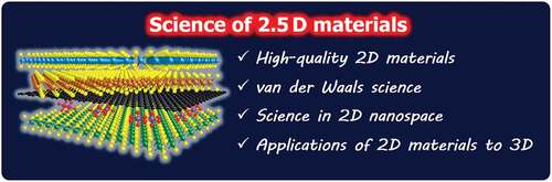
ABSTRACT
The past decades of materials science discoveries are the basis of our present society – from the foundation of semiconductor devices to the recent development of internet of things (IoT) technologies. These materials science developments have depended mainly on control of rigid chemical bonds, such as covalent and ionic bonds, in organic molecules and polymers, inorganic crystals and thin films. The recent discovery of graphene and other two-dimensional (2D) materials offers a novel approach to synthesizing materials by controlling their weak out-of-plane van der Waals (vdW) interactions. Artificial stacks of different types of 2D materials are a novel concept in materials synthesis, with the stacks not limited by rigid chemical bonds nor by lattice constants. This offers plenty of opportunities to explore new physics, chemistry, and engineering. An often-overlooked characteristic of vdW stacks is the well-defined 2D nanospace between the layers, which provides unique physical phenomena and a rich field for synthesis of novel materials. Applying the science of intercalation compounds to 2D materials provides new insights and expectations about the use of the vdW nanospace. We call this nascent field of science ‘2.5 dimensional (2.5D) materials,’ to acknowledge the important extra degree of freedom beyond 2D materials. 2.5D materials not only offer a new field of scientific research, but also contribute to the development of practical applications, and will lead to future social innovation. In this paper, we introduce the new scientific concept of this science of ‘2.5D materials’ and review recent research developments based on this new scientific concept.
GRAPHICAL ABSTRACT
1. Introduction
Materials science is essential to our lives, because many advanced materials are used in, for example, electronics, automobiles, energy production and storage, healthcare, and information technologies. Graphene, a two-dimensional carbon sheet with single-atom thickness, was first prepared by Geim and Novoselov in 2004 using the so-called ‘Scotch tape method’ [Citation1]. Monolayer graphene has attracted great interest from many researchers because it shows unusual physical phenomena, such as ultrahigh carrier mobility, the quantum Hall effect, and massless Dirac fermions [Citation2]. In addition, many applications based on graphene have been proposed including flexible touch panels, integrated circuits, high-frequency transistors, sensors (chemical, biochemical, optical, and magnetic), gas barrier films, templates, and filter membranes – taking advantages of graphene’s high electrical conductivity and high carrier mobility, optical transparency, mechanical strength, and chemical stability [Citation3].
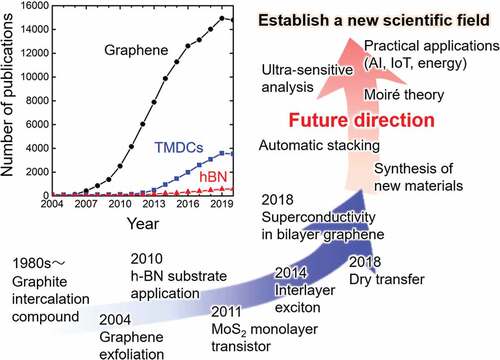
The discovery of graphene opened up a new research field — 2D materials. There are a number of 2D materials with different compositions: transition metal dichalcogenides (TMDCs), hexagonal boron nitride (hBN), and monoelement atomic sheets including silicene (Si), germanene (Ge), stanene (Sn), and black phosphorous (P) [Citation4,Citation5]. Theoretically, more than 1800 types of 2D crystals are predicted [Citation6]. These 2D materials show unique physical properties that strongly depend on their chemical compositions and the number of layers. For example, molybdenum disulfide (MoS2) has an indirect band gap in the bulk crystal, but the monolayer form shows a direct bandgap in the visible range. Monolayer MoS2 also exhibits valley freedom and piezoelectricity. summarizes the research trends of 2D materials and the expected future research directions. Many exciting findings and achievements based on 2D materials have been reported. Therefore, as shown in the inset of , the number of scientific publications has increased with time, reflecting this increased interest in 2D materials.
Figure 1. Trends and future directions of 2D materials research. Inset shows the number of publications about graphene, TMDCs, and hBN (the number of scientific papers whose titles contain each word was counted based on the ISI Web of Science database).
More importantly, now we are able to stack different 2D materials artificially by using advanced transfer techniques [Citation7,Citation8]. This means that we can control weak van der Waals (vdW) interactions so that the materials that can be stacked are no longer limited by lattice constant or composition. In addition, we can control the stacking angle once we know the orientation of the 2D crystals. These techniques essentially provide a new method to synthesize 2D crystals, thus offering new opportunities for breakthroughs in materials science. Some examples of stacking of two graphene sheets are presented in . While monolayer graphene has no band gap, AB-stacked bilayer graphene (BLG) shows a band gap in the presence of a vertical electric field, making it an interesting material for application in semiconductor devices [Citation9]. In contrast, taking advantage of the ability to change the stacking angle, twisted BLG (TBG) with a stacking angle of 1.1° shows a superconducting state at ⁓1 K which originates in the formation of a flat band owing to the long periodicity of the moiré superlattice [Citation10]. The interlayer 2D nanospace, which is sandwiched by π-electrons of graphene, also provides an interesting platform for new materials science. We recently found that unique 2D superstructures of AlCl3 molecules, which are completely different from the structure of a bulk AlCl3 crystal, appear in the BLG interlayer space [Citation11]. Exotic physical properties, such as interlayer excitons, interlayer p-n junction, interlayer tunnelling, and moiré excitons, have been demonstrated using stacks of 2D materials [Citation12–15].
Figure 2. Schematic showing the scientific importance of stacking 2D materials. (a) monolayer graphene, (b) BLG. When stacked with the same angle, i.e. AB-stacking, the BLG shows band gap opening in the presence of vertical electric field, which is useful for semiconductor applications. (d) When the BLG is twisted with a magic angle (~1.1°), it becomes superconducting at low temperature. Reproduced with permission from Springer Nature [Citation10]. (e) in the interlayer 2D nanospace of the BLG, new structures or new materials can be obtained. Reproduced with permission from Wiley-VCHCitation11.
![Figure 2. Schematic showing the scientific importance of stacking 2D materials. (a) monolayer graphene, (b) BLG. When stacked with the same angle, i.e. AB-stacking, the BLG shows band gap opening in the presence of vertical electric field, which is useful for semiconductor applications. (d) When the BLG is twisted with a magic angle (~1.1°), it becomes superconducting at low temperature. Reproduced with permission from Springer Nature [Citation10]. (e) in the interlayer 2D nanospace of the BLG, new structures or new materials can be obtained. Reproduced with permission from Wiley-VCHCitation11.](/cms/asset/4c89fb00-7d80-4f35-accf-5fb1e146d2eb/tsta_a_2062576_f0002_oc.jpg)
We believe that the advancement of such integrated 2D materials will strongly impact materials science. As illustrated in , there are symbiotic possibilities in the space between bulk 3D materials and 2D materials. We call these new materials and architectures ‘2.5D materials,’ where the 0.5D expresses the new dimension created by combining 2D materials through artificial manipulations, such as stacking, twisting, and connecting as well as through the 2D nanospace within 2D material stacks.
Figure 3. Our new concept of ‘2.5D materials.’ There is a large space to develop materials science between conventional 3D bulk materials and layered 2D materials.
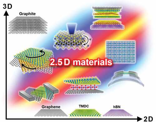
The term ‘2.5D materials’ also covers the integration of 2D materials with other dimensional materials – molecules and ions (zero-dimensional (0D)), nanotubes and nanowires (one-dimensional (1D)), and bulk crystals (three-dimensional (3D)). New research based on our 2.5D materials is expected to bring about a paradigm shift in materials science. The term ‘2.5D materials’ also means applications of 2D materials to our daily life, which is 3D. We can expect advances in 2.5D materials research to impact on many fields including IoT, artificial intelligence (AI), quantum computing, and energy production/storage/efficiency, thus contributing to our society.
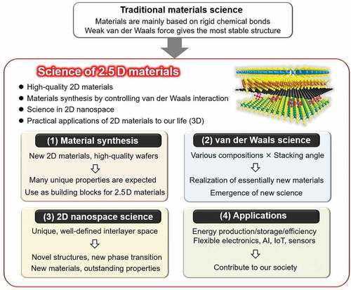
Unlike traditional materials science, in which materials are synthesized based on rigid chemical bonds, in 2.5D materials the weak vdW interaction contributes to form solid materials. While self-assembly also provides materials based on vdW interactions, it generally gives the energetically most stable structure. The main difference is that our approach can control the stacking angle and stacked materials artificially in a highly controlled manner. Synthesizing new layered bulk materials via stacking massive numbers of 2D materials (such as 1,000–10,000 sheets) is challenging but is important to explore a new field of materials science. Inserting different 2D materials periodically in such bulk, layered materials is expected to greatly modify their electrical and optical properties. For this purpose, developing an artificial and automated stacking technology for large-area 2D materials is highly required. Although the transfer technique has been developed recently [Citation8], the instruments are limited to small-scale stacking systems. In addition, the method to transfer a number of 2D materials without wrinkles and bubbles needs to be developed in order to clean interface for effective van der Waals interlayer coupling.
shows an overview of the science of 2.5D materials, which includes four important research topics:
Material synthesis: making new 2D materials as building blocks of various 2.5D materials. In addition, production of high-quality, large 2D material wafers, such as hBN sheets, is also important.
van der Waals science: both vertical stacking and in-plane connection of 2D materials. In the former, combining different types of 2D materials with controlled stacking angles is expected to offer new phenomena, such as moiré physics, to establish a new scientific field. As there are infinite combinations of materials, theories that can predict the physical properties of new 2.5D materials are needed.
2D nanospace: intercalation of molecules and ions to alter the physical properties of the host 2D materials, thus obtaining new ordered structures that could offer novel physical properties and phenomena. Moreover, 2D nanospace offers a unique reaction field for the growth of novel materials that cannot be obtained in usual environments.
Applications: Solar cells, batteries, flexible devices, quantum devices, and devices with very low energy consumption are expected.
Figure 4. Details of science on ‘2.5D materials.’ The research topics and purposes are displayed. The difference between the traditional materials science research and the proposed 2.5D materials research is also explained.
In this article, we review recent scientific studies based on our newly proposed 2.5D materials science and present our perspective on the future of this exciting aspect of materials science.
2. Synthesis and chemistry of 2.5D materials
The growth and transfer of individual 2D materials are key processes for the fabrication of 2.5D materials. Among the various growth methods, chemical vapor deposition (CVD) is widely used to prepare large-area single crystals of 2D materials as well as their polycrystalline films. This will be focused on in Section 2.1. The CVD methods allow the synthesis of various 2D materials on substrates, and advanced CVD techniques can also grow in-plane and stacked 2.5D materials. However, stacking of 2D materials to prepare 2.5D materials has been more widely studied due to its simplicity. The state-of-art stacking methods are also discussed. This is followed by an overview of theoretical approaches to the design of various 2.5D materials, with an emphasis on predicting the effects of intercalation on materials properties (Section 2.2). Methods to intercalate molecules and ions in the interlayer nanospace as well as physical properties and applications of these hybrid systems are presented in Section 2.3.
2.1. CVD growth and assembly for 2.5D materials
This section reviews the studies on the CVD growth and transfer techniques used for typical 2D materials including graphene, hBN, and TMDCs. CVD process has been used to fabricate both vertical (stacked) and in-plane heterostructures of these 2D materials. In addition, the transfer technique enables the creation of vertical heterostructures, including twisted bilayers.
In the case of graphene, CVD growth has mainly been conducted on metal surfaces that effectively decompose hydrocarbons, such as methane, through surface catalytic reactions [Citation16,Citation17]. In addition to the surface reactivity, the carbon solubility of metals is a major factor in controlling the number of graphene layers. For example, Cu foil is frequently used to grow monolayer graphene because of its very low carbon solubility [Citation17], which facilitates the growth of large single crystals of monolayer graphene () [Citation18]. Recently, large-areas, fold-free films of single-crystal monolayer graphene were obtained by using Cu-Ni foil [Citation19]. By increasing the Ni concentration in the Cu-Ni alloy, bilayer graphene, which can be regarded as the simplest form of 2.5D materials, has been also synthesized as a result of the high carbon solubility in the alloy and the suppression of the self-limiting property [Citation20–22]. Similar CVD growth on metal surfaces has been also conducted for monolayer and multilayer hBN [Citation23,Citation24]. In these studies borazine and ammonia borane are widely used as the precursor of hBN. Highly-uniform multilayer hBN was achieved on a Ni–Fe alloy film, which greatly improved the optical property of monolayer WS2 grown on the hBN surface, when compared with that grown on a SiO2 substrate [Citation25]. A 10 × 10 cm2 single-crystal monolayer hBN was reported to epitaxially grow on a Cu (110) vicinal surface [Citation26]. CVD-grown graphene and hBN can be transferred from metal substrates to other substrates, such as silicon wafers, by the polymer-assisted transfer process [Citation23,Citation27].
Figure 5. Growth and assembly of 2D materials. SEM images of (a) single-crystal monolayer graphene grown on Cu foil and (b) in-plane heterostructure of monolayer graphene and hBN grown on Cu foil. Reproduced with permission from American Chemical Society [Citation18] and IOP Publishing [Citation40]. (c) STM image of monolayer MoS2/WS2 in-plane heterostructure. Reproduced with permission from American Chemical Society [Citation44]. (d) SEM image of monolayer WS2-WSe2 in-plane superlattice. Reproduced with permission from AAAS [Citation46]. (e) Optical microscope images of wafer-scale monolayer (left) and a three-layer (right) MoS2 films obtained by the layer-by-layer transfer process. Reproduced with permission from Springer Nature [Citation55]. (f) Robotic transfer system consisting of an optical microscope, stamping apparatus, and chip transfer system. (g) 29 alternating layers of graphene/hBN vertical vdW superlattice obtained by the robotic system shown in (f). Reproduced with permission from Springer Nature [Citation8]. Scale bars are (a) 0.2 mm, (b) 5 μm, (c) 1 nm, (d) 200 nm, and (g) 20 μm.
![Figure 5. Growth and assembly of 2D materials. SEM images of (a) single-crystal monolayer graphene grown on Cu foil and (b) in-plane heterostructure of monolayer graphene and hBN grown on Cu foil. Reproduced with permission from American Chemical Society [Citation18] and IOP Publishing [Citation40]. (c) STM image of monolayer MoS2/WS2 in-plane heterostructure. Reproduced with permission from American Chemical Society [Citation44]. (d) SEM image of monolayer WS2-WSe2 in-plane superlattice. Reproduced with permission from AAAS [Citation46]. (e) Optical microscope images of wafer-scale monolayer (left) and a three-layer (right) MoS2 films obtained by the layer-by-layer transfer process. Reproduced with permission from Springer Nature [Citation55]. (f) Robotic transfer system consisting of an optical microscope, stamping apparatus, and chip transfer system. (g) 29 alternating layers of graphene/hBN vertical vdW superlattice obtained by the robotic system shown in (f). Reproduced with permission from Springer Nature [Citation8]. Scale bars are (a) 0.2 mm, (b) 5 μm, (c) 1 nm, (d) 200 nm, and (g) 20 μm.](/cms/asset/5c8921c7-211d-473f-8b73-5e5d91c44848/tsta_a_2062576_f0005_oc.jpg)
Unlike graphene and hBN, highly-crystalline monolayer TMDCs can be directly synthesized on various non-metallic substrates, including SiO2 [Citation28], sapphire [Citation29], graphene/graphite [Citation30,Citation31], and hBN [Citation32]. In early reports, monolayer TMDCs were frequently grown by CVD with transition metal oxides (such as MoO3 and WO3) and chalcogens (S, Se, and Te). These metal oxides usually require high temperatures ranging from 650–1100°C for the CVD process because of their low vapor pressures. More recently, metal and chalcogen precursors with high vapor pressures were also adopted to produce wafer-scale, uniform polycrystalline films of TMDC monolayers at lower growth temperatures by the metal-organic CVD (MOCVD) method [Citation33]. Wafer-scale single crystals of TMDCs have been recently synthesized by using single-crystalline substrates [Citation34] or seed crystals [Citation35]. In addition to such surface growth, CVD growth of TMDCs occurs at the vdW interface between Au and SiO2 substrate surface, because the metal and chalcogen precursors can diffuse even at their interface [Citation36].
In-plane heterostructures of 2D materials are one of the interesting groups of 2.5D materials. Such in-plane heterostructures were first demonstrated for monolayer graphene and hBN, where hBN grows from the edge of monolayer graphene by CVD () [Citation37–40]. In this process, boron-carbon bonds are preferentially formed at the lateral graphene-hBN interface, resulting in orientation-selective hBN growth from the graphene edge [Citation40]. A similar growth process has been developed to produce in-plane heterostructures consisting of monolayer TMDCs, such as MoS2, WS2, MoSe2, and WSe2 [Citation41–43]. A scanning tunnelling microscopy and scanning tunneling spectroscopy (STM/STS) study revealed an interface with atomically-sharp zigzag edges and a steep band offset around the interface in a MoS2-WS2 in-plane heterostructure () [Citation44]. Due to their composition-dependent band alignment [Citation45], such semiconducting TMDC heterojunctions are particularly promising for future applications in electronics. Furthermore, the multistep and controlled growth of different TMDCs also enables the formation of ultranarrow nanoribbons and lateral superlattices () [Citation44,Citation46].
Like in-plane heterostructures, vertical heterostructures can be also obtained by CVD. In 1984, Koma et al. reported that layered NbSe2 can be epitaxially grown on a MoS2 substrate, despite the large lattice mismatch of about 20%, introducing the concept of vdW epitaxy [Citation47]. The vdW epitaxy has been observed in the CVD growth of various 2D materials, including graphene on hBN [Citation48], and TMDC on graphene [Citation31] (and on graphite [Citation30], hBN [Citation32], and TMDC [Citation43]). Apart from vdW epitaxy, twisted bilayers are also frequently formed via the overlap of two monolayers with different orientations during growth, which has been characterized with electron and optical microscopies for graphene [Citation49] and MoS2 [Citation50]. It is noted that the growth of vertical heterostructures allows the formation of clean, atomically-flat vdW interfaces without any contaminations or wrinkle/bubble formation, overcoming some common problems in the transfer process described below. For example, CVD-grown TMDCs on graphite or hBN showed uniform photoluminescence (PL) with very narrow linewidths because of the suppression of unintentional lattice strain and carrier doping [Citation30,Citation32].
Nonetheless, the transfer process is the most used way to prepare vertical heterostructures by layer-by-layer stacking of 2D materials. In particular, hBN crystals have been widely used as insulating substrates with clean and atomically flat surfaces for other 2D materials [Citation51]. Monolayer graphene on hBN shows higher carrier mobilities than it does on SiO2 substrates [Citation52]. In recent years, the dry transfer process has been frequently used to stack multiple 2D materials to make, for example, a hBN/graphene/hBN vertical heterostructure [Citation53]. Furthermore, to control the twist angle between two layers, the ‘tear and stack’ process of a single crystal of 2D material has been developed [Citation54]. Wafer-scale vertical heterostructures with high uniformity were obtained by the layer-by-layer transfer of polycrystalline TMDC films grown by CVD (), in which bubble and wrinkle formation were suppressed by transferring in vacuum [Citation55]. To create more complex vertical heterostructures, a robotic searching and assembly system was recently developed, as shown in [Citation8]. This system allows the preparation of a vertical vdW superlattice consisting of 29 alternating layers of graphene and hBN () [Citation8]. Similar robotic assembly was also developed to produce an artificially-stacked material containing 80 layers of MoS2 made from the patterned CVD-grown MoS2 monolayers [Citation56].
As shown above, the growth and transfer techniques have been advancing rapidly to fabricate various artificial structures based on 2D materials. In particular, the CVD process enables the syntheses of wafer-scale single crystals and superlattices of ultranarrow nanoribbons of 2D materials. The progress in transfer technique has also enabled moiré superlattices in twisted bilayers. A variety of 2.5D materials will be pioneered by the combination of these techniques and by applying them to other materials not only 2D materials.
2.2. Theoretical design of novel 2.5D materials
In this section, physical phenomena associated with the non-integer dimensionality (that is, the additional 0.5D) are discussed from the theoretical view point, together with theoretical predictions and design of novel 2.5D materials. Low-dimensional nanomaterials intrinsically possess hierarchical structures with themselves or other materials, where they act as elemental units, like atoms do in conventional solids [Citation57–61]. Owing to the chemically-inert surfaces of the constituent nanomaterials, such as graphene and other 2D materials, large spacing between the constituent materials are inherent to such hierarchical structures, leading to an additional degree of freedom with which to tailor their physical properties. This additional degree of freedom endows such hierarchical materials with non-integer dimensionality. From the theoretical viewpoint, several pioneering works pointed out the importance of such non-integer dimensionality.
Graphene and other 2D materials are known to possess peculiar unoccupied electron states (nearly free electron (NFE) state or interlayer band); such states have their maxima in the vacuum space outside the 2D layered materials, as shown in [Citation61–64]. Upon intercalating atomic layers of alkali or alkali-earth atoms between graphene layers, the NFE state shifts downward, owing to the attractive potential caused by metal ions, and crosses the Fermi level; this leads to superconductivity which would not have been expected from the simple sum of the electronic properties of the graphene layers and intercalated atomic layers [Citation62].
Figure 6. (a) Contour plots of the wave function of the lowest (left panel) and the second lowest (right panel) NFE states of an isolated graphene. The number shows the square of the wave function. Linear plots indicate the corresponding densities. Reproduced with permission from American Physical Society [Citation62]. (b) an optimised structure of dibenzo-corannulene sandwiched by two graphene layers. Grey and pink balls denote C atoms belonging to graphene and dibenzo-corannulene, respectively, and white balls are H atoms. Reproduced with permission from American Chemical Society [Citation63]. (c) Schematics of C60-graphene co-intercalation compound (left panel) and K-doped C60-graphene co-intercalation compound (right panel). Large, medium, and small balls denote C60 molecules, K atoms, and C atoms, respectively. Reproduced with permission from American Physical Society [Citation64]. (d) Isosurfaces of electron-depleted (blue) and accumulated (yellow) regions of sumanene-intercalated bilayer graphene and the charge density distribution along z-axis. Reproduced with permission from American Chemical Society [Citation67]. (e) Geometric structure and spin density of a copolymer of phenalenyl and phenyl groups. Reproduced with permission from Elsevier [Citation68]. (f) Geometric structure of polymerized trypticene. Reproduced with permission from the Physical Society of Japan [Citation69]. (g) Schematics of wave functions of the edge states at k=π, 8π/9, 7π/9, and 2π/3 (left to right). Reproduced with permission from IOP Publishing [Citation70].
![Figure 6. (a) Contour plots of the wave function of the lowest (left panel) and the second lowest (right panel) NFE states of an isolated graphene. The number shows the square of the wave function. Linear plots indicate the corresponding densities. Reproduced with permission from American Physical Society [Citation62]. (b) an optimised structure of dibenzo-corannulene sandwiched by two graphene layers. Grey and pink balls denote C atoms belonging to graphene and dibenzo-corannulene, respectively, and white balls are H atoms. Reproduced with permission from American Chemical Society [Citation63]. (c) Schematics of C60-graphene co-intercalation compound (left panel) and K-doped C60-graphene co-intercalation compound (right panel). Large, medium, and small balls denote C60 molecules, K atoms, and C atoms, respectively. Reproduced with permission from American Physical Society [Citation64]. (d) Isosurfaces of electron-depleted (blue) and accumulated (yellow) regions of sumanene-intercalated bilayer graphene and the charge density distribution along z-axis. Reproduced with permission from American Chemical Society [Citation67]. (e) Geometric structure and spin density of a copolymer of phenalenyl and phenyl groups. Reproduced with permission from Elsevier [Citation68]. (f) Geometric structure of polymerized trypticene. Reproduced with permission from the Physical Society of Japan [Citation69]. (g) Schematics of wave functions of the edge states at k=π, 8π/9, 7π/9, and 2π/3 (left to right). Reproduced with permission from IOP Publishing [Citation70].](/cms/asset/80ce5720-5442-4093-bb9d-084c200e48ab/tsta_a_2062576_f0006_oc.jpg)
Graphene and graphite can also form hybrid structures with molecules, such as fullerene (C60) and hydrocarbon molecules. In such hybrid structures, guest molecules are predicted to have 2D condensed forms which are rarely observed in their bulk phases. In addition, the confined nanoscale spacing between the graphene layers gives the novel molecular conformations that would be unstable under the ambient conditions. For example, as shown in , a curved molecule, dibenzo-corannulene, becomes flat when enclosed in the two graphene layers [Citation63]. A hybrid structure comprising C60 and graphite has been theoretically designed as a novel all-carbon compound with mixed dimensionality () [Citation64]. The electronic structures of the host graphene and guest C60 molecules are highly modulated when they are incorporated into these hybrid structures. Charge redistribution occurs by the substantial orbital hybridization between the NFE state of graphene and π states of C60. Another interesting possibility is sumanene, a bowl-shaped hydrocarbon molecule (C21H12) [Citation65,Citation66], which could form hybrid structures with graphene, offering unique electronic properties (). The electronic structure of the hybrid structures strongly depends on the sumanene conformation (i.e. whether it is ‘bowl’ or ‘flat’ [Citation67]). When the sumanene molecule has the bowl shape between graphene layers, the dipole moment normal to the molecular plane of sumanene causes charge transfer, leading to electron and hole codoping in upper and lower graphene layers, respectively, with electron and hole densities of approximately 1012/cm2 () [Citation67].
Covalent networks of hydrocarbon molecules are a new type of 2.5D materials which have unique physical properties. show representative examples. As a result of the internal degree of freedom, a carbon-based network derived from phenalenyl and phenyl groups has a Dirac cone and Kagome bands at and above/below the Fermi level, respectively, owing to these constituent units and their arrangements () [Citation68]. Furthermore, two-dimensionally polymerized triptycene has Kagome bands at valence and conduction band edges, even though this covalent network contains sp3-hybridized carbon atoms () [Citation69].
Structural imperfections in covalent networks also play crucial roles in determining physical and optoelectronic properties of nanomaterials. An early theoretical calculation predicted that the graphene edges causes specific edge-localized electronic states (edge states) when the edge has a zigzag shape. This gives unique flat-band states at the Fermi level () [Citation70,Citation71]. This result implies that the imperfections give an additional degree of freedom for the electronic properties of the resultant structures [Citation68,Citation72]. For example, in-plane heterostructures of graphene and hBN possess localized electronic states at the zigzag border between the two materials. In this case, the edge states of graphene and hBN hybridize each other at the zigzag border, resulting in the formation of bonding and antibonding edge states at their border [Citation73,Citation74].
2.3. Intercalation for the synthesis of 2.5D materials
Stacks of 2D materials provide unique well-defined 2D nanospace that is sandwiched by adjacent layers. As illustrated in , this 2D nanospace can be used to intercalate molecules and ions, analogous to the extensively studied graphite-intercalation-compounds (GICs). In GICs, intercalation significantly alters the electrical, magnetic, and optical properties of the host graphite [Citation57]. Similarly, the intercalation allows us to engineer the physical properties of host 2D materials. Thus, the intercalated 2D materials can be regard as ‘2.5D materials’.
Figure 7. Intercalation in stacked 2D materials. (a) Concept of the intercalation within 2D nanospace. (b,c) Schematic and Raman spectra of monolayer, bilayer, and few-layer graphene intercalated with FeCl3 molecules. Reproduced with permission from Wiley-VCH [Citation75]. There are two different graphene sheets with different doping levels; G1 and G2 indicate lower and higher doping levels, respectively. (d) Sheet resistance change of MoCl5-intercalated BLG stored in ambient condition. Reproduced with permission from Wiley-VCH (modified from ref. [Citation79]). The BLG was grown by CVD method, and, by tuning the growth condition, AB- and twist-rich BLG were selectively synthesized. (e) Temperature dependence of the resistance of Ca-intercalated BLG grown on SiC. Reproduced with permission from American Chemical Society [Citation81]. (f) Atomic models of Li ions stored in graphite (left) and BLG (right). Reproduced with permission from Springer Nature [Citation83]. The simulation suggests higher density of Li in the BLG. (g) Illustration of Na intercalation in chemically modified graphene stacks. Reproduced with permission from AAAS [Citation85]. Monolayer graphene sheets functionalized with 4-NBD molecules are stacked to form an electrode for the intercalation. (h) New AlCl3 structures observed inside the interlayer space of CVD-grown BLG. Reproduced with permission from Wiley-VCH [Citation11]. (i) Intercalation of magnetic Co ions in the interlayer of TaS2 with the assistant of TBAC molecules. Reproduced with permission from Wiley-VCH [Citation89]. (j) TEM images of atomic layers of Ga, In, Sn formed at the interface between graphene and SiC substrate. Right graph shows the magnetic field dependence of the superconductivity of the Ga layer. Reproduced with permission from Springer Nature [Citation92].
![Figure 7. Intercalation in stacked 2D materials. (a) Concept of the intercalation within 2D nanospace. (b,c) Schematic and Raman spectra of monolayer, bilayer, and few-layer graphene intercalated with FeCl3 molecules. Reproduced with permission from Wiley-VCH [Citation75]. There are two different graphene sheets with different doping levels; G1 and G2 indicate lower and higher doping levels, respectively. (d) Sheet resistance change of MoCl5-intercalated BLG stored in ambient condition. Reproduced with permission from Wiley-VCH (modified from ref. [Citation79]). The BLG was grown by CVD method, and, by tuning the growth condition, AB- and twist-rich BLG were selectively synthesized. (e) Temperature dependence of the resistance of Ca-intercalated BLG grown on SiC. Reproduced with permission from American Chemical Society [Citation81]. (f) Atomic models of Li ions stored in graphite (left) and BLG (right). Reproduced with permission from Springer Nature [Citation83]. The simulation suggests higher density of Li in the BLG. (g) Illustration of Na intercalation in chemically modified graphene stacks. Reproduced with permission from AAAS [Citation85]. Monolayer graphene sheets functionalized with 4-NBD molecules are stacked to form an electrode for the intercalation. (h) New AlCl3 structures observed inside the interlayer space of CVD-grown BLG. Reproduced with permission from Wiley-VCH [Citation11]. (i) Intercalation of magnetic Co ions in the interlayer of TaS2 with the assistant of TBAC molecules. Reproduced with permission from Wiley-VCH [Citation89]. (j) TEM images of atomic layers of Ga, In, Sn formed at the interface between graphene and SiC substrate. Right graph shows the magnetic field dependence of the superconductivity of the Ga layer. Reproduced with permission from Springer Nature [Citation92].](/cms/asset/b3f4a60e-d36c-4e5b-a4e4-301a9036f504/tsta_a_2062576_f0007_oc.jpg)
The simplest 2D host material is bilayer graphene (BLG). FeCl3 molecules were intercalated into exfoliated BLG and few-layer graphene (FLG) in early studies [Citation75–78], because FeCl3 is relatively easy to handle in ambient conditions owing to its stability. The intercalation of FeCl3 induces hole doping in the BLG and significantly reduces the sheet resistance of the host BLG. Compared with the widely used surface doping of graphene, higher stability is expected for intercalated materials, because the intercalants are protected by graphene layers. In the case of BLG and FLG, the intercalation can be monitored by the shift of the Raman G-band, which is sensitive to the carrier density. As shown in , the G-band upshifts to higher wavenumbers with increasing carrier concentration [Citation75]. The graphene sandwiched by FeCl3 layers (G2 in ) shows a larger G-band shift than that of the graphene which only faces FeCl3 on one side (G1). The ability to evaluate the doping degree using Raman spectroscopy is a strong advantage of graphene – in other 2D materials it is not as easy to determine their doping levels.
In the previous research, most of the BLG and FLG was prepared by exfoliation of bulk graphite. This limits the size and stacking order of the resulting graphene; exfoliation gives small graphene flakes with mostly AB stacking order. Kinoshita et al. investigated the intercalation of MoCl5 molecules in large-area BLG sheet which was grown by CVD [Citation79]. As shown in , they discovered that TBG with high twist angles is more amenable to intercalation than BLG with AB stacking, resulting in lower sheet resistance of the intercalated TBG. This can be accounted for by the weaker interlayer coupling in large-angle TBG. Because the CVD growth gives a large BLG sheet, it was possible to fabricate large-area organic solar cells using intercalated BLG instead of an indium tin oxide (ITO) electrode [Citation79]. The low sheet resistance of FLG obtained by MoCl5 intercalation enabled its use as interconnects to replace commercial Cu wires [Citation80]. Because Ca-GIC shows the highest superconducting-transition temperature (Tc) of 11.5 K among GICs, BLG was also used to intercalate Ca ions [Citation81]. By using BLG grown on a SiC substrate, Ichionokura et al. prepared Ca-intercalated BLG, which showed a superconductor transition at 2–4 K () [Citation81]. Although the Tc is lower than that reported for Ca-GIC, there is a still chance to increase the Tc by using hBN substrate or other approaches. Graphene layers were also used as a template as well as a protecting layer for NbSe2 2D superconductor [Citation82].
Relevant to energy storage, Kühne fabricated an electrochemical monitoring setup and found superdense ordering of Li ions in BLG with a much higher Li density than that seen in Li-GIC (C6Li) () [Citation83]. The same group also reported that the diffusion rate of Li ions in BLG is much faster than that in graphite [Citation84]. These interesting results open a new opportunity to produce high-performance rechargeable batteries based on 2.5D materials. It is known that graphite cannot host Na ions, even though Na-ion batteries are expected to be cheaper and to use more abundant resources than the current Li-ion batteries. Recently, by stacking CVD-graphene that had been functionalized with 4-nitrobenzene diazonium tetrafluoroborate (4-NBD) and reduced, the intercalation of Na ions has been realized [Citation85]. depicts how the 2D nanospace that had been expanded by the 4-NBD molecule enables the intercalation of bulky Na ions, while attracting them to the -NH2 groups.
It is noted that 2D nanospace can offer a unique stage to explore materials science. One example can be found in the work by Y.-C. Lin et al. [Citation11]. They intercalated AlCl3 molecules into CVD-BLG and observed their atomic structures using a scanning transmission electron microscope (STEM). Interestingly, they discovered three new AlCl3 crystalline structures in the interlayer 2D nanospace as shown in , which are completely different from the structure of the bulk AlCl3 crystal [Citation11,Citation86]. In addition, these structures showed phase transitions upon excitation by an electron beam. The reason for these new crystalline structures is not clear, but it may be related to the surrounding π-electrons and/or a pressure effect suggested for the molecules confined between the graphene layers [Citation87]. Experimental finding of such new structures demonstrates the potential of 2D nanospace and the strong impact on traditional GIC research. Graphene-based liquid cells that contain liquid, such as water, between graphene layers can be also regarded as 2.5D systems. Such cells enable in situ observation of liquid phase reactions inside a transmission electron microscope (TEM) [Citation88].
The use of 2D nanospace is not limited to BLG and FLG. For example, Li et al. proposed ‘imprinting’ ferromagnetism by intercalating magnetic metals into layered TaS2 () [Citation89]. Given that tetrabutylammonium chloride (TBAC) can be intercalated into a TaS2 crystal, they facilitated the cointercalation of Co ions into TaS2 layers by dissolving CoCl2 in the TBAC solution. This allowed the experimental observation of the magnetic properties of the Co-intercalated TaS2. An electrochemical method has also been used to intercalate molecules into MoS2 layers [Citation90]. Interestingly, the intercalation of cetyltrimethylammonium bromide (CTAB) induced the phase transition of MoS2 from the semiconducting 2 H phase to the semimetallic 1T phase; these are examples where both the intercalant and the host 2D material offer unique physical and chemical properties.
As well as the interlayer spaces within 2D materials, the nanospace between the 2D material and substrate surface is also an interesting place to intercalate molecules and solid materials. Hayashi et al. reported the synthesis of 2D Sn at the graphene-SiC interface [Citation91]. Later, Briggs et al. demonstrated the formation of 2D Ga, In, or Sn layers at the interface by applying plasma treatment (which gave entry pores for these elements) prior to the evaporation [Citation92]. shows cross-sectional TEM images of these 2D monoatomic layers. Moreover, the 2D Ga layer exhibited a superconducting transition, which showed different behavior from that of Ga bulk crystals, suggesting that the 2D Ga layer confined in 2D nanospace is unique.
3. Physical properties of 2.5D materials
Stacking of two layers of 2D materials brings out novel physical properties that cannot be expected from each of the constituents. This is because we have new degrees of freedom, such as combination of 2D materials, stacking (twist) angles, and valleys, which are obtained through the stacking of layered materials by the methods described in Section 2.1. In other words, the possibility of the control of van der Waals interaction makes 2.5D materials unique and exciting. In particular, twist angles or different lattice constants in stacked bilayers give moiré superlattices which open a new scientific field. In this section we focus on new physics brought by moiré superlattices in stacked bilayers, followed by the experimental observations of intriguing physical properties that have appeared in various types of 2.5D materials.
3.1. Moiré physics in 2.5D materials
Moiré superlattices are a novel type of nanoscale materials in which individual 2D materials are stacked on top of each other without lattice matching. A striking feature of this class of materials is that physical properties are strongly dependent on the moiré pattern caused by the interference of the lattice structures. The moiré period, typically a few to tens of nanometers, significantly modifies the band structure of the host materials, giving rise to a number of remarkable properties that cannot be observed without stacking. In the following, we review recent scientific studies on various moiré superlattices.
A typical example of moiré superlattice is TBG [Citation10,Citation93–103], in which, as described earlier, a pair of graphene layers are rotationally stacked with an arbitrary twist angle (). The moiré period of TBG is inversely proportional to the twist angle, and is ⁓15 nm at 1 degree. In the electronic structure of TBG, the Dirac cones of individual graphene layers are strongly hybridized by the superlattice interlayer coupling (), and the electronic spectrum is rearranged into a series of moiré subbands (). Generally, the energy width of the moiré subbands decreases as the twist angle is reduced, and, at a so-called ‘magic angle’ near 1 degree, a dispersionless ‘flat band’ appears [Citation94]. Remarkably, the magic angle TBG exhibits superconductivity when the flat band is partially filled ()) [Citation10,Citation99–101]. The superconductivity is believed to be caused by the electron-electron interaction and the band flatness. In a flat band, generally, the kinetic energy is quenched, and hence the physical properties are dominated by the electron-electron interaction. Besides the superconductivity, magic angle TBG shows various phases depending on the electron density, including correlated insulating phases [Citation10,Citation99–101] and magnetic phases [Citation102,Citation103], which are all expected to originate from electron-electron interactions. The superconductivity and correlated phases have been also found in other moiré graphene systems, such as twisted double bilayer graphene (i.e. a twisted pair of AB-stacked bilayer graphene) [Citation104–109], and twisted trilayer graphene [Citation110–113], where the band flatness is assumed to be essential, as it is in TBG.
Figure 8. (a) Atomic structures of TBG with different twist angles. (b) Schematics of the Brillouin-zone (BZ) folding of TBG (10 degree), where red and blue hexagons represent the BZ of individual graphene layers, and small black hexagons are that of the moiré superlattice. (c) Band structures of low-angle TBG. Reproduced with permission from American Physical Society [Citation98]. (d) (Top) Longitudinal resistance plotted against carrier density at different perpendicular magnetic fields from 0 T (black trace) to 480 mT (red trace). (Bottom) Color plot of longitudinal resistance measured against carrier density and temperature, showing different phases including metal, band insulator (BI), correlated state (CS) and superconducting state (SC). Reproduced with permission from Springer Nature [Citation101]. (e) A false-colored TEM image of 30-degree TBG mapped with 12-fold Stampfli-inflation tiling. Reproduced with permission from AAAS [Citation127].
![Figure 8. (a) Atomic structures of TBG with different twist angles. (b) Schematics of the Brillouin-zone (BZ) folding of TBG (10 degree), where red and blue hexagons represent the BZ of individual graphene layers, and small black hexagons are that of the moiré superlattice. (c) Band structures of low-angle TBG. Reproduced with permission from American Physical Society [Citation98]. (d) (Top) Longitudinal resistance plotted against carrier density at different perpendicular magnetic fields from 0 T (black trace) to 480 mT (red trace). (Bottom) Color plot of longitudinal resistance measured against carrier density and temperature, showing different phases including metal, band insulator (BI), correlated state (CS) and superconducting state (SC). Reproduced with permission from Springer Nature [Citation101]. (e) A false-colored TEM image of 30-degree TBG mapped with 12-fold Stampfli-inflation tiling. Reproduced with permission from AAAS [Citation127].](/cms/asset/10e1d366-1d5d-4b61-934d-aaddf89a2ee9/tsta_a_2062576_f0008_oc.jpg)
The moiré superlattice is not limited to graphene. For instance, a twisted stack of TMDCs also gives a moiré superlattice with unusual optical properties. A monolayer of TMDC (e.g. MoS2, MoSe2, WS2, WSe2) is a direct band gap semiconductor in which an optically excited electron-hole pair forms an exciton. When two monolayers of TMDC are rotationally stacked, an optical excitation gives rise to localized excitons trapped by the moiré pattern [Citation12,Citation114,Citation115]. These trapped excitons could be applied to information storing devices.
Another well studied moiré superlattice is a composite system of graphene and hBN, where the slightly different lattice constants of graphene and hBN makes a 15 nm moiré pattern without rotation [Citation116–118]. Here, the graphene’s Dirac cone is strongly modulated by an effective potential induced by the hBN, resulting in formation of minigaps in the Dirac cone [Citation119,Citation120–123]. When the Fermi energy locates in a minigap, the system exhibits the valley Hall effect [Citation124]. This is the Hall effect analogue which occurs in the absence of magnetic field, where electrons of the K and K’ valleys of graphene move in opposite directions perpendicular to an applied electric field. This phenomenon is attributed to the emergent Berry curvature induced by the inversion-symmetry breaking potential from hBN. It was also reported that superconductivity is observed in ABC-stacked trilayer graphene on hBN, where flat bands are formed in ABC-graphene’s band by the hBN superlattice modulation [Citation125].
Most of the 2D superlattices reported in the literature, including the examples presented above, are characterized by long-range moiré patterns (~ tens of nm) which are much longer than periods of atoms in crystals. Theoretically, such systems can be treated by an effective moiré theory [Citation93–97], which extracts the moiré length period while coarse-graining the atomic-scale structures. However, when the twist angle is too large, or the atomic periods of the host materials are not close to each other, the long-range and short-range length scales cannot be separated. Then, the system becomes essentially quasiperiodic, in which incommensurate periodicities coexist, and the Bloch theory is not applicable [Citation126]. A representative example of this situation is a 30-degree rotated twisted BLG, which can be fabricated by an epitaxial growth on a SiC surface [Citation127]. As shown in , the system has the striking feature of a 12-fold rotational symmetric quasicrystal, which is intimately related to quasiperiodic tiling in mathematics [Citation127,Citation128]. Also, quasiperiodic features generally emerge in trilayer systems, such as hBN/graphene/hBN [Citation129–136], where two moiré patterns coexist.
In these non-periodic situations, theoretical description of physical properties is limited by the inapplicability of the Bloch theorem. There have been several theoretical attempts to describe the electronic structure of quasiperiodic 2D superlattices. For the 30-degree TBG mentioned above, the 12-fold rotational symmetric electronic structure can be successfully described by quasi-bands defined in quasi momentum space [Citation128]. Quite recently, it was shown that energy gaps in 2D quasiperiodic systems can generally be characterized by a set of topological numbers called the second Chern numbers, which can be interpreted as quantized integers in the high-dimensional quantum Hall effect [Citation137]. These concepts serve as a fundamental framework to describe the physical properties in quasiperiodic twisted 2D systems, where the Bloch theory is not applicable. The above-mentioned, highly controlled nanoscale architectures consisting of 2D materials, such as graphene, hBN, and TMDC, that exhibit extraordinarily properties can also be categorized as 2.5D materials.
3.2. Physical properties of 2.5D materials
The novel physical properties that emerge at the nanoscale interface between the atomically thin 2D materials in vdW heterostructures are an important research topic for both science and application of 2.5D materials. Artificial vdW heterostructures based on semiconducting 2D materials have been most widely studied because of their importance in electronics and photonics [Citation138–140]. The valley degrees of freedom coupled with the spin (spin-valley locking) in the monolayer semiconductor enables selective circularly polarized excitations and emissions from optically generated excitonic states (excitons and trions) at the equivalent K (−K) valley without magnetic fields [Citation141,Citation142]. The interface between monolayer semiconducting and magnetic materials in the vdW heterostructures provides a novel platform for investigating optically excited states with spin-valley locking properties. shows a schematic of an artificial vdW heterostructure composed of a monolayer semiconductor (WSe2) and a ferromagnetic insulating material (CrI3) [Citation143]. The vdW heterostructure (WSe2/CrI3) exhibits large energy splitting of excitonic states (valley-Zeeman splitting) and emission of circularly-polarized light (valley-spin polarization) due to breaking of valley degeneracy under the effective magnetic field [Citation144] arising from local-spins in ferromagnetic CrI3 (). A similar result was also reported for a vdW heterostructure with a different ferromagnetic insulator, EuS () [Citation145]. The interaction of valley spin-polarized excitons (trions) and ferromagnetic spins can be further enhanced and controlled via proximity magnetic-exchange effects. The tunable valley-spin polarization and large valley-Zeeman splitting with the hBN thickness at the interfaces (i.e. spacer layer) have been demonstrated in the vdW heterostructure of a semiconductor monolayer (MoSe2) and a ferromagnetic, perovskite transition metal oxide ((La.8Nd.2)1.2Sr1.8Mn2O7), as shown in [Citation146].
Figure 9. (a) Schematic of the artificial heterostructure of semiconducting monolayer (WSe2) and magnetic material (CrI3). Reproduced with permission from AAAS [Citation143]. (b) Spectrum showing circularly-polarized PL from excitonic states in monolayer WSe2, which suggests valley-Zeeman splitting induced by a magnetic proximity effect from the ferromagnetic CrI3. Reproduced with permission from AAAS [Citation143]. (c) Valley-Zeeman splitting induced by a magnetic proximity effect from ferromagnetic EuS. Reproduced with permission from Springer Nature [Citation145]. (d) Schematic of vdW heterostructure of a semiconductor monolayer (MoSe2) and a perovskite transition metal oxide ((La.8Nd.2)1.2Sr1.8Mn2O7) with a hBN layer. Reproduced with permission from Wiley-VCH [Citation146]. (e) Large valley-Zeeman splitting and polarization in monolayer MoSe2 on perovskite Mn oxide. Reproduced with permission from Wiley-VCH [Citation146]. (f) Schematic of the atomic arrangement in the moiré superlattice formed in a heterobilayer with twist angle θ. Reproduced with permission from Springer Nature [Citation114]. (g) Low temperature PL spectra of moiré superlattice in MoSe2/WSe2 heterobilayer, measured at low (blue: 20 nW) and high (dark red: 10 µw) optical power densities. Inset shows an expanded energy scale of a sharp PL spectral line, with linewidth ~100 μeV. Reproduced with permission from Springer Nature [Citation114]. (h) 2D photoluminescence excitation (PLE) map. The two-resonance excess energies of 24 and 48 meV are indicated by the black dashed lines. Reproduced with permission from American Chemical Society [Citation13].
![Figure 9. (a) Schematic of the artificial heterostructure of semiconducting monolayer (WSe2) and magnetic material (CrI3). Reproduced with permission from AAAS [Citation143]. (b) Spectrum showing circularly-polarized PL from excitonic states in monolayer WSe2, which suggests valley-Zeeman splitting induced by a magnetic proximity effect from the ferromagnetic CrI3. Reproduced with permission from AAAS [Citation143]. (c) Valley-Zeeman splitting induced by a magnetic proximity effect from ferromagnetic EuS. Reproduced with permission from Springer Nature [Citation145]. (d) Schematic of vdW heterostructure of a semiconductor monolayer (MoSe2) and a perovskite transition metal oxide ((La.8Nd.2)1.2Sr1.8Mn2O7) with a hBN layer. Reproduced with permission from Wiley-VCH [Citation146]. (e) Large valley-Zeeman splitting and polarization in monolayer MoSe2 on perovskite Mn oxide. Reproduced with permission from Wiley-VCH [Citation146]. (f) Schematic of the atomic arrangement in the moiré superlattice formed in a heterobilayer with twist angle θ. Reproduced with permission from Springer Nature [Citation114]. (g) Low temperature PL spectra of moiré superlattice in MoSe2/WSe2 heterobilayer, measured at low (blue: 20 nW) and high (dark red: 10 µw) optical power densities. Inset shows an expanded energy scale of a sharp PL spectral line, with linewidth ~100 μeV. Reproduced with permission from Springer Nature [Citation114]. (h) 2D photoluminescence excitation (PLE) map. The two-resonance excess energies of 24 and 48 meV are indicated by the black dashed lines. Reproduced with permission from American Chemical Society [Citation13].](/cms/asset/2daa60ab-afd9-4717-a7a5-83b8f8d60660/tsta_a_2062576_f0009_oc.jpg)
The universal phenomena of overlapping and tilting of two similar periodic patterns are frequently seen in our daily life, and are called moiré interference patterns, as described in the previous section. Moiré quantum interferences across a wide range from the atomic (or nano)- to macro-scale play an important role in science, such as in superconducting quantum interference devices [Citation147], superconductivity in solids [Citation10,Citation100], and others [Citation102]. The moiré physics in the interference of twist-stacked atomically thin 2D materials provides novel effects that are not seen in other materials; finding such effects is one of the important research targets in the science and engineering of 2.5D materials. The moiré pattern arising from the spatially varying atomic registry, as shown in , causes periodic trap potential for excitons in vdW heterostructures made by twisted stacking of two semiconductor monolayers [Citation12,Citation114,Citation115,Citation148].
shows typical low-temperature PL spectra of a MoSe2/WSe2 heterobilayer, measured at low (blue: 20 nW) and high (red: 10 µW) optical power densities [Citation114]. Several sharp lines are clearly observed in the PL spectrum under the excitation power density of 20 nW. The inset shows a single sharp (linewidth ~100 μeV) PL spectral line on an expanded energy scale. The extremely sharp and randomly distributed PL peaks in the spectra stem from recombination of excitons trapped in a moiré potential (moiré excitons), which are very different to the broader emission peak from 2D excitons in the spectrum of monolayer WSe2 (MoSe2). The precise energies of excitons trapped in the moiré potential well, which are sensitively affected by the small differences in local environment in each potential well, have a Gaussian distribution. A Gaussian broadened peak, with multiple smaller sharp peaks, was observed in the PL spectrum under the high optical power density (10 µW), because each moiré potential well is occupied by excitons.
The PL excitation (PLE) spectra provide complementary information about the optical absorption of moiré excitonic systems. shows the 2D PLE spectral map of a MoSe2/WSe2 heterobilayer, collected from the resonant PL spectra as a function of excitation photon energies [Citation13]. The PLE map suggests that the PL spectrum change strongly depends on the excitation energy, and that the optical absorption occurs under near-resonant conditions. Significant PLE signals were observed near the tilted dashed lines with excess energies of ~ 24 and ~48 meV, where the excess energy is defined by the difference between emission and excitation photon energy. The energy difference of 24 meV observed in the PLE resonance is close to the energy of the phonon modes in MoSe2 and WSe2, suggesting that the moiré excitons resonantly couple with their phonons.
The precise probing techniques that have been developed to examine the nanoscale interface and moiré excitonic systems formed in novel vdW heterostructures will also contribute to the emergence of new physical properties and further understanding of the physics of 2.5D materials.
4. Applications of 2.5D materials
In the previous chapter, we discussed the science of 2.5D materials, mainly focusing on their synthesis and physical properties. Integration of various 2D materials with controlled angles, stacking of a large number of 2D materials (e.g. >100 layers with controlled compositions), intercalation in the interlayer nanospace, 3D macrostructures made of 2D layered materials – all these can be considered as 2.5D materials – have enormous potential for applications, such as quantum information, electronics, automobiles, energy, biotechnology, and environmental protection. In addition, most of the applications of 2D materials require solid substrates (3D materials) in which interface engineering is essential to bring out the intrinsic physical properties of the 2D materials. Therefore, mixing or integration of materials across dimensions is also crucial for the future development of potential applications. In this section we focus on electronic, energy, and photonic applications of 2.5D materials, all of these take advantage of their unique geometrical structures and physical properties.
4.1. Electronic applications of 2.5D materials
There are three dominant research directions for electronic applications of 2.5D materials. The first is next-generation complementary metal oxide semiconductor (CMOS) and memory technologies based on 2D materials integration. The most advanced transistor today is a fin-type field effect transistor (Fin-FET) [Citation149–151], which can enhance gate-controllability and reduce power consumption. To further advance the technology node, the nanosheet gate-all-around (NS-GAA) structure is intensively investigated by reducing the thickness of fin width. Recently, the NS-GAA structure based on 2D heterostructures of MoS2/hBN/graphene was demonstrated [Citation152], as shown in . 2.5D heterostructures offer two main advantages here: one is their atomically thin (less than 1 nm) channel thickness, which cannot be reached with the conventional Si system; the other is that the surfaces of 2D materials are free of dangling bonds so that the hetero-interfaces are electrically inert. [Citation153–156]. Therefore, the highest performance in terms of subthreshold swing (SS) and current on/off ratio has been realized, significantly improved over that of GAA structures containing conventional 3D channels made from Si, Ge, and other semiconductors. For memory technology, 2.5D heterostructures have been extensively investigated for next-generation non-volatile memory (NVM) devices, because very high electrical reliability is expected thanks to the electrically inert hetero-interface [Citation157,Citation158]. Recently, the memory operation mechanisms behind the round sweep-transfer curves have been revealed based on the systematic comparison of inherent floating gate voltage trajectories for three different 2D channels [Citation159]. Moreover, ultrafast program/erase operation (~20 ns) has been demonstrated, as shown in [Citation160,Citation161]. Compared with the non-volatile floating-gate-type Si flash memory whose operation speed is the order of microseconds [Citation162], 2.5D heterostructured NVMs are now knocking on the door of storage-class memory, with an operation speed close to that of working memory.
Figure 10. (a) Schematic 2D nanosheet heterostructure (left) and current on/off ratio as a function of SS (right). Reproduced with permission from Wiley-VCH [Citation152], the references referred in the right panel can be found in this reference). (b) Ultrafast program/erase operation in MoS2/hBN/multilayer graphene heterostructure NVM. Reproduced with permission from Springer Nature [Citation160]. (c) SS lower than thermodynamic limitation of 60 mV/dec achieved in n-MoS2/p+-MoS2 TFET heterostructured with hBN. Reproduced with permission from American Chemical Society (modified from ref. [Citation14]). (d) Schematic illustration of a BP/MoSe2 heterojunction device and response of three sensors as a function of NO2 gas concentration. Reproduced with permission from IOP Publishing [Citation166]. (e) an all-carbon device fabricated on a flexible PEN substrate and magnified image of a 21-stage ring oscillator. Reproduced with permission from Springer Nature [Citation171].
![Figure 10. (a) Schematic 2D nanosheet heterostructure (left) and current on/off ratio as a function of SS (right). Reproduced with permission from Wiley-VCH [Citation152], the references referred in the right panel can be found in this reference). (b) Ultrafast program/erase operation in MoS2/hBN/multilayer graphene heterostructure NVM. Reproduced with permission from Springer Nature [Citation160]. (c) SS lower than thermodynamic limitation of 60 mV/dec achieved in n-MoS2/p+-MoS2 TFET heterostructured with hBN. Reproduced with permission from American Chemical Society (modified from ref. [Citation14]). (d) Schematic illustration of a BP/MoSe2 heterojunction device and response of three sensors as a function of NO2 gas concentration. Reproduced with permission from IOP Publishing [Citation166]. (e) an all-carbon device fabricated on a flexible PEN substrate and magnified image of a 21-stage ring oscillator. Reproduced with permission from Springer Nature [Citation171].](/cms/asset/cb661c6a-a7eb-47e2-adb5-e4031af33988/tsta_a_2062576_f0010_oc.jpg)
The second research direction is the ultra-low power consumption, which cannot be achieved by next-generation CMOS technology because of the thermodynamically limited steepness of the transfer characteristics in the subthreshold regime; that is, the SS is limited to be larger than 60 mVdec−1 at room temperature [Citation161]. To overcome this limitation, two major concepts for steep-slope devices have been proposed: negative-capacitance (NC) FETs [Citation163] and tunnel FETs (TFETs) [Citation164]. TFETs are more feasible for 2.5D materials because the device design, which is based on the band-to-band tunnelling (BTBT), can be easily implemented by the characteristics of 2D materials – the shorter tunnelling distance owing to the vdW gap and the strong gate controllability owing to the atomically thin channel. All-2D-heterostructure TFETs (which may be called 2.5D-TFETs) produced by combining a type III n-MoS2/p+-MoS2 heterostructure with a hBN top gate insulator resulted in SS values lower than 60 mVdec−1 at room temperature, as shown in [Citation14]. Further reductions in SS values and higher on-currents are possible when the entire hetero-interface is more rigorously controlled [Citation165].
The third research direction is toward multifunctionality, to create, for example, sensors, transducers, and flexibility devices. As shown in , using the 2.5D heterostructure of black phosphorus (BP) and MoSe2 layers, a highly sensitive gas sensor was demonstrated [Citation166]. In general, a monolayer 2D channel is used as the sensing interface to provide an enhanced surface to volume ratio [Citation167,Citation168]. Here, the heterojunction demonstrates a considerably lower detection limit, ~25 ppb, and higher sensitivity toward nitrogen dioxide (NO2); this occurs because chemical adsorption can induce significant changes in band alignment and carrier transport behavior (). 2.5D heterostructures provide a new platform for sensing applications, where the different 2D materials that make up the heterostructure can actively and independently interact with target molecules and contribute to the sensing process. Moreover, flexibility is one of the advantages of 2.5D materials, some of which can accommodate strains exceeding 10%, giving an additional functionality to electronic applications [Citation169,Citation170]. displays an all-carbon device fabricated on a flexible polyethylene naphthalate (PEN) substrate [Citation171]. This flexible device is fully transparent because the typical Au electrodes were replaced by carbon nanotube electrodes. Such transparency will drastically increase the range of applications. Although shows carbon nanotube device, the integration of the tubular materials (1D materials) with 2D materials [Citation154] or inserting 1D materials within 2D nanospace [Citation172] can open up a new paradigm for nanoscale material systems.
Finally, from the viewpoint of electronic applications of 2.5D materials, there is one issue which needs to be addressed, that is the smaller relative dielectric constant of multilayer hBN (~3) compared with that of SiO2 (3.9), which limits the usage of hBN as a gate insulator in ultrascaled CMOS devices [Citation173]. Although enhancement of the capacitance by combining monolayer hBN and a high-k oxide is one of the possible solutions, a better option is likely to be exploring new 2D insulators, which would lead to a wide variety of applications without reducing the performance of 2.5D materials.
4.2. Energy and optoelectronic applications of 2.5D materials
2.5D materials are also being actively studied for application in energy conversion devices and optoelectronic devices. In TMDCs stacked with vdW heterojunctions, photoexcited electrons and holes are charge-separated via interfacial charge transfer. It is noted that monolayer TMDC shows a high light absorption efficiency of 5–10%, which is about 10 times higher than that of Si or GaAs [Citation174]. Therefore, TMDC heterojunctions are expected to be applied in flexible photovoltaic cells and photodetectors. In addition, TMDC heterostructures are expected to be useful as catalysts and ion transfer membranes due to efficient electron transfer between the adjacent layers that are coupled by vdW interaction [Citation175,Citation176]. As well as this, TMDC and graphene can be applied to various energy conversion and light-emitting devices, where they offer new functions, such as plasmons and intercalation. They may also be used in optoelectronic devices in combination with 2D organic and inorganic hybrid lead halide perovskites (2D-PVSK). In this section, we review recent progress on the energy and optoelectronic applications of various 2.5D materials.
In a photovoltaic device with a simple heterostructure of MoS2 and WS2, MoS2 acts as an electron acceptor and WS2 acts as an electron donor for charge separation. The unique point here is that the absorption spectrum is not a simple sum of the absorption spectra of the two materials – the existence of charge transfer excitons is predicted from theoretical calculations [Citation174]. Furchi et al. constructed a MoS2/WSe2 photovoltaic system shown in , and demonstrated the photovoltaic effect with an open circuit voltage of about 0.5 V () [Citation177]. Light is absorbed by both WSe2 and MoS2, and excitons are generated in both monolayers. Due to the spatial separation of the lowest energy electron and hole states, electronic excitation occurs across the heterojunction, followed by lateral diffusion of the generated carriers along the interface as shown in the inset of [Citation177]. Interlayer recombination is supposed to occur during the carrier diffusion, reducing the photocurrent. Interestingly, Tan et al. theoretically proposed that charge recombination can be suppressed by inserting a 2–3 nm thick hBN insulating layer between the MoS2 and WSe2 and that the photoelectric conversion efficiency (PCE) of MoS2/hBN/WSe2 photovoltaic devices can be approximately doubled. They theoretically predicted that the PCE exceeding 23% could be obtained by increasing the TMDC thickness and optimizing the hBN thickness [Citation178].
Figure 11. (a) Schematic illustration of the TMDC bilayer photovoltaic device. Reproduced with permission from American Chemical Society [Citation177]. (b) J−V curves of the device shown in (a) measured under illumination of 180, 400, 670, 1100, 1800, 4000, and 6400 W/m2 (in the order of red to blue). Reproduced with permission from American Chemical Society [Citation177]. (c) Schematic illustration of GLG. Reproduced with permission from Springer Nature [Citation181]. (d) Schematic diagram of monolayer MoS2 plasmonic photoFets under bias and illumination with a gate voltage. Reproduced with permission from American Chemical Society [Citation184]. (e) Photoresponsivity of the plasmonic photoFET and bare monolayer MoS2 photoFET as a function of illumination wavelength. The red curve shows reflection spectrum of the plasmonic nanostructures. Reproduced with permission from American Chemical Society [Citation184].
![Figure 11. (a) Schematic illustration of the TMDC bilayer photovoltaic device. Reproduced with permission from American Chemical Society [Citation177]. (b) J−V curves of the device shown in (a) measured under illumination of 180, 400, 670, 1100, 1800, 4000, and 6400 W/m2 (in the order of red to blue). Reproduced with permission from American Chemical Society [Citation177]. (c) Schematic illustration of GLG. Reproduced with permission from Springer Nature [Citation181]. (d) Schematic diagram of monolayer MoS2 plasmonic photoFets under bias and illumination with a gate voltage. Reproduced with permission from American Chemical Society [Citation184]. (e) Photoresponsivity of the plasmonic photoFET and bare monolayer MoS2 photoFET as a function of illumination wavelength. The red curve shows reflection spectrum of the plasmonic nanostructures. Reproduced with permission from American Chemical Society [Citation184].](/cms/asset/9c2123f5-4b73-4684-a3e8-01285706a5de/tsta_a_2062576_f0011_oc.jpg)
A MoS2/MoTe2 photovoltaic system using MoTe2 as an electron donor exhibited the photovoltaic effect with an open circuit voltage of 0.3 V by near-infrared light (800 nm) [Citation179]. This can be explained by the charge separation mechanism based on the type-II band alignment, which is similar to the research by Furchi et al [Citation177]. High-performance photovoltaic devices were also fabricated using a few-layer ReS2/monolayer WSe2 stack, achieving 1.5% PCE with a fill factor of 0.56 [Citation180], an important step towards increasing the performance of flexible solar cells.
In a further example, BLG can be used to create a promising electrode material with high conductivity and transparency, by intercalating molecules and ions between the graphene layers. As already shown in , intercalating MoCl5 molecules into twist-rich BLG significantly reduced the sheet resistance (83 Ω Ω−1), allowing to apply it to organic solar cells with a high PCE [Citation79]. Graphene-like graphite (GLG, , which has a 2D stacked, porous graphitic structure with chemically introduced C-O-C units, was applied as the anode in a Li-ion battery. The GLG electrode showed a large capacity of 608 mAh/g at the upper cell voltage limit of 2 V [Citation181]. In contrast, MoS2 and MoSe2 nanosheets were applied as cathodes with Mg plate anodes for hybrid Mg-Li ion batteries [Citation182]. The stacked structure of carbon-stabilized heat-expanded TMDC is expected to find applications in both the anode and cathode of carbon-free Li-ion batteries. Furthermore, MoS2 thin films are attracting interest as photoelectrodes for hydrogen evolution through water reduction because of their high light absorbance and high electrochemical activity [Citation183].
Stacked structures of TMDC and metallic nanostructures that show localized surface plasmon resonances are another example of 2.5D materials that are expected to be used in light-energy conversion devices and optoelectronic devices. Lan et al. placed silver nanostructures on monolayer MoS2 to construct a gate-tunable plasmonic phototransistor (photoFET), as shown in [Citation184]. The constructed plasmonic photoFET showed high photoresponsiveness, with a 7.2-fold increase (over that of the control non-plasmonic FET) at the plasmon resonance wavelength (). This is accounted for by the effective use of photons arising from the plasmon optical antenna effect and plasmon-induced photocarrier generation [Citation184]. On the other hand, the electromagnetic field enhancement effect of the plasmons was also utilized for the light-emitting devices. Actually, the efficiency of the light-emitting devices was improved by exploiting the PL enhancement of MoS2 by plasmons [Citation185,Citation186].
The 2.5D materials were applied not only to the photovoltaic devices but also to the light-emitting devices. In 2.5D materials science, it is possible to engineer band structures of materials by stacking various two-dimensional materials in a highly controlled manner. Even for light-emitting devices, stacking of mechanically exfoliated 2D materials ensures high quality in each of TMDC monolayers, so that high performance is generally obtained as a total device [Citation187]. Withers et al. succeeded in demonstrating a light-emitting device with an external quantum efficiency (EQE) of 5% at room temperature by sandwiching a single layer WSe2 with h-BN tunnel barrier layers and top and bottom transparent graphene electrodes, () [Citation188]. Interestingly, the WSe2-based light-emitting device showed much higher EQE at room temperature than that of the MoSe2 device (). They showed different temperature dependence, which was explained by the inverted sign of spin−orbit splitting of conduction band states in WSe2 and MoSe2 [Citation188].
Figure 12. (a) Schematic of a light-emitting device sandwiching a single layer of WSe2 between hBN barrier layers with top and bottom transparent graphene electrodes. High-resolution TEM image and energy-dispersive X-ray analysis of a cross-section of the device. Reproduced with permission from American Chemical Society [Citation188]. (b) Electroluminescence spectra taken at different temperatures for WSe2 and MoSe2 light-emitting devices with hBN tunnel barriers measured with applied bias of 2 V and 1.8 V, respectively. Reproduced with permission from American Chemical Society [Citation188]. (c) PL spectra of single-layer WSe2, MoS2, and WSe2/MoS2 hetero-bilayer. Reproduced with permission from National Academy of Sciences [Citation189]). (d) Energy diagram of WSe2/MoS2 hetero-bilayer under photoexcitation. Reproduced with permission from National Academy of Sciences [Citation189]. (e) Electroluminescence from the WSe2/MoS2 hetero-bilayer light-emitting device. Reproduced with permission from American Chemical Society [Citation139]. (f) Optical image of the bilayer-WS2/2D-PVSK (n = 4) heterostructure on a SiO2/Si substrate. Reproduced with permission from American Chemical Society [Citation193]). (g) Photoluminescence spectra of the bare bilayer-WS2 (red line), the bare 2D-PVSK (n = 4) (blue), and bilayer-WS2/2D-PVSK heterostructure (black). The excitation wavelength is 514 nm. Reproduced with permission from American Chemical Society [Citation193].
![Figure 12. (a) Schematic of a light-emitting device sandwiching a single layer of WSe2 between hBN barrier layers with top and bottom transparent graphene electrodes. High-resolution TEM image and energy-dispersive X-ray analysis of a cross-section of the device. Reproduced with permission from American Chemical Society [Citation188]. (b) Electroluminescence spectra taken at different temperatures for WSe2 and MoSe2 light-emitting devices with hBN tunnel barriers measured with applied bias of 2 V and 1.8 V, respectively. Reproduced with permission from American Chemical Society [Citation188]. (c) PL spectra of single-layer WSe2, MoS2, and WSe2/MoS2 hetero-bilayer. Reproduced with permission from National Academy of Sciences [Citation189]). (d) Energy diagram of WSe2/MoS2 hetero-bilayer under photoexcitation. Reproduced with permission from National Academy of Sciences [Citation189]. (e) Electroluminescence from the WSe2/MoS2 hetero-bilayer light-emitting device. Reproduced with permission from American Chemical Society [Citation139]. (f) Optical image of the bilayer-WS2/2D-PVSK (n = 4) heterostructure on a SiO2/Si substrate. Reproduced with permission from American Chemical Society [Citation193]). (g) Photoluminescence spectra of the bare bilayer-WS2 (red line), the bare 2D-PVSK (n = 4) (blue), and bilayer-WS2/2D-PVSK heterostructure (black). The excitation wavelength is 514 nm. Reproduced with permission from American Chemical Society [Citation193].](/cms/asset/c176a0f1-7dc8-4faf-bf0a-6034aa145ce2/tsta_a_2062576_f0012_oc.jpg)
Hetero-bilayers of TMDC, such as WSe2/MoS2 system, has been well studied for the light-emitting device with analogous to photovoltaic devices. Single-layer WSe2 and MoS2 show PL spectra peaking at 1.64 eV and 1.87 eV, respectively, as shown in . The WSe2/MoS2 hetero-bilayer gives the PL at 1.55 eV, which is related to the energy difference between the conduction band of MoS2 and the valence band of WSe2. Their band diagram is presented in [Citation189]. By utilizing a hetero-bilayer of WSe2/MoS2 stack, Cheng et al. have successfully demonstrated the electroluminescence (EL) device () [Citation139].
Combinations of 2D-PVSK and TMDCs are other 2.5D materials that are also attracting attention for use in light-emitting devices. Erkılıç et al. succeeded in synthesizing the heterostack of 2D-PVSK and monolayer WS2 by all vapor phase deposition and observed the strong coupling between these different types of 2D materials from the modulation of their PL characteristics [Citation190]. Optical transistors consisting of 2D-PVSK and WS2 have also been fabricated, and their efficient photovoltaic effects were investigated [Citation191,Citation192]. These materials also have some disadvantages – TMDCs have low quantum efficiencies, due to defect states and band-to-band transitions from direct to indirect, while 2D-PVSK is unstable in ambient atmosphere. Yang et al. reported that charge transfer states are formed when 2 L-WS2 is stacked on 2D-PVSK as shown in ; the PL intensity is increased by two orders of magnitude compared with that of bare WS2 and the stability is improved compared with that of bare 2D-PVSK () [Citation193]. Although this approach is still in its infancy, many studies have found that the characteristics of energy and optoelectronic devices can be improved by using 2.5D material systems.
5. Conclusions and future perspectives
In this review, we explain our novel concept of 2.5D materials science by reviewing recent publications. This concept, which will further extend the current research on 2D materials, includes the synthesis of high-quality 2D materials and their wafers, sophisticated control of the stacking of various 2D materials, stacking of massive numbers of 2D materials with clean interfaces, finding and understanding novel phenomena, exploration of the science in interlayer 2D nanospace, integration of 2D materials with materials having different dimensions, and advanced research for applications to our life (3D). In addition to theoretical studies and calculations, other techniques, such as machine learning, deep learning, and materials informatics should be also incorporated to design and predict new 2.5D materials that exhibit outstanding properties and promising properties. As shown in , there are many opportunities to explore new materials science, and potentially have a strong impact on our future life. This new concept also requires strong collaborations between researchers working in different fields. Through such collaborative research on the basis of ‘2.5D materials,’ we believe that the new scientific field will be established which lead to a new era of materials science.
Figure 13. Future prospects of science of ‘2.5D materials.’
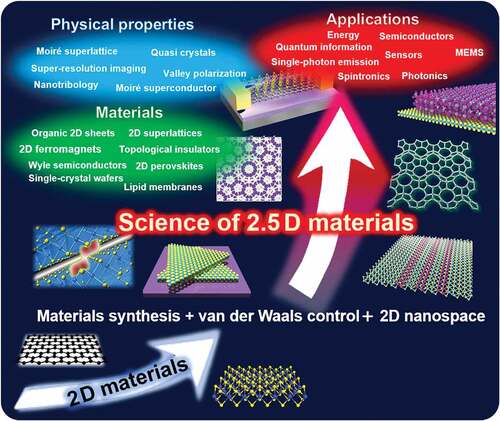
Acknowledgments
We thank Prof. Yukiko Takamura for helpful discussion.
Disclosure statement
No potential conflict of interest was reported by the author(s).
Additional information
Funding
Notes on contributors

Hiroki Ago
Hiroki Ago is a distinguished professor at the Global Innovation Center (GIC) at Kyushu University. He received his Ph.D. from Kyoto University in 1997. After spending one and a half years at the Cavendish Laboratory, Cambridge University, he became a researcher at the Nanocarbon Research Center of the National Institute for Advanced Industrial Science and Technology (AIST) at Tsukuba. In 2003, he joined the Institute for Materials Chemistry and Engineering, Kyushu University as an associate professor. In 2016, he became a full professor at the Global Innovation Center, Kyushu University. Now, he is a leader of the Grant-in-Aid for Transformative Research Area, ‘Science of 2.5 Dimensional Materials’, supported by the MEXT, Japan. His current research focuses on the controlled synthesis and growth mechanisms of various two-dimensional materials and the investigation of their novel properties as well as the development of applications.

Susumu Okada
Susumu Okada is a professor in the Department of Physics at the University of Tsukuba. He received his Ph.D. from Tokyo Institute of Technology in 1998 for a theoretical study on geometric and electronic properties of fullerene molecules and polymerized fullerenes. After his PhD, he joined the Institute of Material Science at the University of Tsukuba as an assistant professor, and moved to the Department of Physics in 2001. His current research focuses on the geometric and electronic properties of nanoscale materials.

Yasumitsu Miyata
Yasumitsu Miyata is an associate professor at the Department of Physics at Tokyo Metropolitan University. He received his Ph.D. in Physics from Tokyo Metropolitan University in 2008. He was a research fellow of the Japan Society for the Promotion of Science (JSPS) (2008-2009), and was an assistant professor at Nagoya University (2009-2013). In 2013, he moved to Tokyo Metropolitan University. His current research is focused on the growth, physical properties, and applications of 2D materials including transition metal dichalcogenides.
Kazunari Matsuda
Kazunari Matsuda is a professor at the Institute of Advanced Energy, Kyoto University. He received his Ph.D. from Nagoya University in 1998 for ultrafast optical spectroscopy of strongly correlated oxide systems. He joined Kanagawa Academy of Science and Technology as a researcher in 1998. He joined the Institute of Chemical Research at Kyoto University as an associate professor in 2004, and was promoted to a full professor at the Institute of Advanced Energy, Kyoto University in 2010. His current research explores novel optical science of various nanomaterials including two-dimensional materials. He is also interested in understanding their novel physical properties as well as the development of optical and energy applications.

Mikito Koshino
Mikito Koshino is a distinguished professor in the Department of Physics at Osaka University. He received his Ph.D. degree from University of Tokyo in 2003. He was a research associate at Tokyo Institute of Technology from 2003 to 2010, and an associate professor at Tohoku University from 2010 to 2016. Since 2016, he has taught at Osaka University. His current research focuses on theoretical study of electronic properties of various low-dimensional materials including graphene and other 2D materials, and the topological materials, such as Weyl-Dirac semimetals and topological insulators.

Kosei Ueno
Kosei Ueno is a professor at the Department of Chemistry, Faculty of Science, Hokkaido University, Japan. He received his Ph.D. degree in Chemistry from Hokkaido University in 2004 for chemical applications of microfluidic devices. From 2004 to 2006, he worked in Professor Hiroaki Misawa’s laboratory as a JSPS research fellow. He became an assistant professor at Hokkaido University in 2006 and was promoted to associate professor in 2008. In 2019, he became a full professor at the Department of Chemistry, Faculty of Science, Hokkaido University. His recent research interests include controlling light and matter interactions using 2.5D materials and their application to energy and optoelectronic devices.

Kosuke Nagashio
Kosuke Nagashio is a professor at the Department of Materials Engineering, The University of Tokyo. He received a B.E. degree in Materials Science and Engineering from Kyoto University in 1997 and M.E. and Ph.D. degrees in Materials Engineering from The University of Tokyo in 1999 and 2002, respectively. From 2002 to 2003, he was a postdoctoral research fellow at Stanford University, California. He is currently a Professor in the Department of Materials Engineering, The University of Tokyo. His current research interests are the carrier transport in 2D materials and the crystal growth of 2D materials. He is a member of the Japan Society of Applied Physics (JSAP), the Materials Research Society (MRS), the IEEE Electron Devices Society (EDS) and the American Physical Society (APS).
References
- Novoselov KS, Geim AK, Morozov SV, et al. Electric field effect in atomically thin carbon films. Science. 2004;306:666–669.
- Geim AK, Novoselov KS. The rise of graphene. Nat Mater. 2007;6:183–191.
- Zurutuza A, Marinelli C. Challenges and opportunities in graphene commercialization. Nat Nanotechnol. 2014;9:730–734.
- Choi W, Choudhary N, Han GH, et al. Recent development of two-dimensional transition metal dichalcogenides and their applications. Mater Today. 2017;20:116–130.
- Mannix AJ, Kiraly B, Hersam MC, et al. Synthesis and chemistry of elemental 2D materials. Nat Rev Chem. 2017;1:0014.
- Mounet N, Gibertini M, Schwaller P, et al. Two-dimensional materials from high-throughput computational exfoliation of experimentally known compounds. Nat Nanotechnol. 2018;13:246–252.
- Pizzocchero F, Gammelgaard L, Jessen BS, et al. The hot pick-up technique for batch assembly of van der Waals heterostructures. Nat Commun. 2016;7:11894.
- Masubuchi S, Morimoto M, Morikawa S, et al. Autonomous robotic searching and assembly of two-dimensional crystals to build van der Waals superlattices. Nat Commun. 2018;9:1413.
- Oostinga JB, Heersche HB, Liu X, et al. Gate-Induced insulating state in bilayer graphene devices. Nat Mater. 2008;7:151–157.
- Cao Y, Fatemi V, Fang S, et al. Unconventional superconductivity in magic-angle graphene superlattices. Nature. 2018;556:43–50.
- Lin Y-C, Motoyama A, Kretschmer S, et al. Polymorphic phases of metal chlorides in the confined 2D space of bilayer graphene. Adv Mater. 2021;33:2105898.
- Jin C, Regan EC, Yan A, et al. Observation of moiré excitons in WSe2/WS2 heterostructure superlattices. Nature. 2019;567:76–80.
- Shinokita K, Miyauchi Y, Watanabe K, et al. Resonant coupling of a Moiré exciton to a phonon in a WSe2/MoSe2 heterobilayer. Nano Lett. 2021;21:5938–5944.
- Nakamura K, Nagamura N, Ueno K, et al. All 2D heterostructure tunnel field-effect transistors: impact of band alignment and heterointerface quality. ACS Appl Mater Interfaces. 2020;12:51598–51606.
- Aji AS, Izumoto M, Suenaga K, et al. Two-step synthesis and characterization of vertically stacked SnS–WS2 and SnS–MoS2 p–n heterojunctions. Phys Chem Chem Phys. 2018;20:889–897.
- Kim KS, Zhao Y, Jang H, et al. Large-scale pattern growth of graphene films for stretchable transparent electrodes. Nature. 2009;457:706–710.
- Li X, Cai W, An J, et al. Large-area synthesis of high-quality and uniform graphene films on copper foils. Science. 2009;324:1312–1314.
- Li X, Magnuson CW, Venugopal A, et al. Large-area graphene single crystals grown by low-pressure chemical vapor deposition of methane on copper. J Am Chem Soc. 2011;133:2816–2819.
- Wang M, Huang M, Luo D, et al. Single-crystal, large-area, fold-free monolayer graphene. Nature. 2021;596:519–524.
- Takesaki Y, Kawahara K, Hibino H, et al. Highly uniform bilayer graphene on epitaxial Cu-Ni(111) alloy. Chem Mater. 2016;28:4583–4592.
- Solís-Fernández P, Terao Y, Kawahara K, et al. Isothermal growth and stacking evolution in highly uniform Bernal-stacked bilayer graphene. ACS Nano. 2020;14:6834–6844.
- Huang M, Bakharev PV, Wang Z-J, et al. Large-area single-crystal AB-bilayer and ABA-trilayer graphene grown on a Cu/Ni(111) foil. Nat Nanotechnol. 2020;15:289–295.
- Song L, Ci L, Lu H, et al. Large scale growth and characterization of atomic hexagonal boron nitride layers. Nano Lett. 2010;10:3209–3215.
- Kim KK, Hsu A, Jia X, et al. Synthesis of monolayer hexagonal boron nitride on Cu foil using chemical vapor deposition. Nano Lett. 2012;12:161–166.
- Uchida Y, Nakandakari S, Kawahara K, et al. Controlled growth of large-area uniform multilayer hexagonal boron nitride as an effective 2D substrate. ACS Nano. 2018;12:6236–6244.
- Wang L, Xu X, Zhang L, et al. Epitaxial growth of a 100-square-centimetre single-crystal hexagonal boron nitride monolayer on copper. Nature. 2019;570:91.
- Li X, Zhu Y, Cai W, et al. Transfer of large-area graphene films for high-performance transparent conductive electrodes. Nano Lett. 2009;9:4359–4363.
- Lee Y-H, Zhang X-Q, Zhang W, et al. Synthesis of large-area MoS2 atomic layers with chemical vapor deposition. Adv Mater. 2012;24:2320–2325.
- Dumcenco D, Ovchinnikov D, Marinov K, et al. Large-area epitaxial monolayer MoS2. ACS Nano. 2015;9:4611–4620.
- Kobayashi Y, Sasaki S, Mori S, et al. Growth and optical properties of high-quality monolayer WS2 on graphite. ACS Nano. 2015;9:4056–4063.
- Shi Y, Zhou W, A-Y L, et al. van der Waals epitaxy of MoS2 layers using graphene as growth templates. Nano Lett. 2012;12:2784–2791.
- Okada M, Sawazaki T, Watanabe K, et al. Direct chemical vapor deposition growth of WS2 atomic layers on hexagonal boron nitride. ACS Nano. 2014;8:8273–8277.
- Kang K, Xie S, Huang L, et al. High-mobility three-atom-thick semiconducting films with wafer-scale homogeneity. Nature. 2015;520:656–660.
- Li T, Guo W, Ma L, et al. Epitaxial growth of wafer-scale molybdenum disulfide semiconductor single crystals on sapphire. Nat Nanotechnol. 2021;16:1201–1207.
- Xu X, Pan Y, Liu S, et al. Seeded 2D epitaxy of large-area single-crystal films of the van der Waals semiconductor 2H MoTe2. Science. 2021;372:195–200.
- Lim HE, Irisawa T, Okada N, et al. Monolayer MoS2 growth at the Au–SiO2 interface. Nanoscale. 2019;11:19700–19704.
- Levendorf MP, Kim C-J, Brown L, et al. Graphene and boron nitride lateral heterostructures for atomically thin circuitry. Nature. 2012;488:627–632.
- Miyata Y, Maeda E, Kamon K, et al. Fabrication and characterization of graphene/hexagonal boron nitride hybrid sheets. Appl Phys Express. 2012;5:085102.
- Sutter P, Cortes R, Lahiri J, et al. Interface formation in monolayer graphene-boron nitride heterostructures. Nano Lett. 2012;12:4869–4874.
- Maeda E, Miyata Y, Hibino H, et al. Orientation-controlled growth of hexagonal boron nitride monolayers templated from graphene edges. Appl Phys Express. 2017;10:055102.
- Duan X, Wang C, Shaw JC, et al. Lateral epitaxial growth of two-dimensional layered semiconductor heterojunctions. Nat Nanotechnol. 2014;9:1024–1030.
- Huang C, Wu S, Sanchez AM, et al. Lateral heterojunctions within monolayer MoSe2–WSe2 semiconductors. Nat Mater. 2014;13:1096–1101.
- Gong Y, Lin J, Wang X, et al. Vertical and in-plane heterostructures from WS2/MoS2 monolayers. Nat Mater. 2014;13:1135–1142.
- Kobayashi Y, Yoshida S, Maruyama M, et al. Continuous heteroepitaxy of two-dimensional heterostructures based on layered chalcogenides. ACS Nano. 2019;13:7527–7535.
- Gong C, Zhang H, Wang W, et al. Band alignment of two-dimensional transition metal dichalcogenides: application in tunnel field effect transistors. Appl Phys Lett. 2013;103:053513.
- Xie S, Tu L, Han Y, et al. Coherent, atomically thin transition-metal dichalcogenide superlattices with engineered strain. Science. 2018;359:1131–1136.
- Koma A, Sunouchi K, Miyajima T. Fabrication and characterization of heterostructures with subnanometer thickness. Microelectron Eng. 1984;2:129–136.
- Yang W, Chen G, Shi Z, et al. Epitaxial growth of single-domain graphene on hexagonal boron nitride. Nat Mater. 2013;12:792–797.
- Havener RW, Zhuang H, Brown L, et al. Angle-resolved Raman imaging of interlayer rotations and interactions in twisted bilayer graphene. Nano Lett. 2012;12:3162–3167.
- Liu K, Zhang L, Cao T, et al. Evolution of interlayer coupling in twisted molybdenum disulfide bilayers. Nat Commun. 2014;5:4966.
- Taniguchi T, Watanabe K. Synthesis of high-purity boron nitride single crystals under high pressure by using Ba–BN solvent. J Cryst Growth. 2007;303:525–529.
- Dean CR, Young AF, Meric I, et al. Boron nitride substrates for high-quality graphene electronics. Nat Nanotechnol. 2010;5:722–726.
- Wang L, Meric I, Huang PY, et al. One-dimensional electrical contact to a two-dimensional material. Science. 2013;342:614–617.
- Cao Y, Luo JY, Fatemi V, et al. Superlattice-induced insulating states and valley-protected orbits in twisted bilayer graphene. Phys Rev Lett. 2016;117:116804.
- Kang K, Lee K-H, Han Y, et al. Layer-by-layer assembly of two-dimensional materials into wafer-scale heterostructures. Nature. 2017;550:229–233.
- Mannix AJ, Ye A, Sung SH, et al. Robotic four-dimensional pixel assembly of van der Waals solids. Nat Nanotechnol. 2022. DOI: 10.1038/s41565-021-01061-5
- Dresselhaus MS, Dresselhaus G. Intercalation compounds of graphite. Adv Phys. 2002;51:1–186.
- Saito S, Oshiyama A. Cohesive mechanism and energy bands of solid C60. Phys Rev Lett. 1991;66:2637–2640.
- Delaney P, Choi HJ, Ihm J, et al. Broken symmetry and pseudogaps in ropes of carbon nanotubes. Nature. 1998;391:466–468.
- Miyamoto Y, Saito S, Tománek D. Electronic interwall interactions and charge redistribution in multiwall nanotubes. Phys Rev B. 2001;65:041402.
- Smith BW, Monthioux M, Luzzi DE. Encapsulated C60 in carbon nanotubes. Nature. 1998;396:323–324.
- Posternak M, Baldereschi A, Freeman AJ, et al. Prediction of electronic surface states in layered materials: graphite. Phys Rev Lett. 1984;52:863–866.
- Denis PA. Pristine graphene-based catalysis: significant reduction of the inversion barriers of adsorbed and confined corannulene, sumanene, and dibenzo[a,g]corannulene. J Phys Chem a. 2015;119:5770–5777.
- Saito S, Oshiyama A. Design of C60-graphite cointercalation compounds. Phys Rev B. 1994;49:17413–17419.
- Sakurai H, Daiko T, Sakane H, et al. Structural elucidation of sumanene and generation of its benzylic anions. J Am Chem Soc. 2005;127:11580–11581.
- Higashibayashi S, Tsuruoka R, Soujanya Y, et al. Trimethylsumanene: enantioselective synthesis, substituent effect on bowl structure, inversion energy, and electron conductivity. Bull Chem Soc Jpn. 2012;85:450–467.
- Maruyama M, Okada S. Carrier redistribution in van der Waals nanostructures consisting of bilayer graphene and buckybowl: implications for piezoelectric devices. ACS Appl Nano Mater. 2021;4:3007–3012.
- Maruyama M, Cuong NT, Okada S. Coexistence of dirac cones and kagome flat bands in a porous graphene. Carbon. 2016;109:755–763.
- Fujii Y, Maruyama M, Okada S. Geometric and electronic structures of two-dimensionally polymerized triptycene: covalent honeycomb networks comprising triptycene and polyphenyl. Jpn J Appl Phys. 2018;57:125203.
- Fujita M, Wakabayashi K, Nakada K, et al. Peculiar localized state at zigzag graphite edge. J Phys Soc Jpn. 1996;65:1920–1923.
- Nakada K, Fujita M, Dresselhaus G, et al. Edge state in graphene ribbons: nanometer size effect and edge shape dependence. Phys Rev B. 1996;54:17954–17961.
- Shima N, Aoki H. Electronic structure of super-honeycomb systems: a peculiar realization of semimetal/semiconductor classes and ferromagnetism. Phys Rev Lett. 1993;71:4389–4392.
- Okada S, Igami M, Nakada K, et al. Border states in heterosheets with hexagonal symmetry. Phys Rev B. 2000;62:9896–9899.
- Maruyama M, Okada S. Magnetic properties of graphene quantum dots embedded in h-BN sheet. J Phys Chem C. 2016;120:1293–1302.
- Zhan D, Sun L, Ni ZH, et al. FeCl3-based few-layer graphene intercalation compounds: single linear dispersion electronic band structure and strong charge transfer doping. Adv Funct Mater. 2010;20:3504–3509.
- Kim N, Kim KS, Jung N, et al. Synthesis and electrical characterization of magnetic bilayer graphene intercalate. Nano Lett. 2011;11:860–865.
- Zhao W, Tan PH, Liu J, et al. Intercalation of few-layer graphite flakes with FeCl3: Raman determination of fermi level, layer by layer decoupling, and stability. J Am Chem Soc. 2011;133:5941–5946.
- Khrapach I, Withers F, Bointon TH, et al. Novel highly conductive and transparent graphene-based conductors. Adv Mater. 2012;24:2844–2849.
- Kinoshita H, Jeon I, Maruyama M, et al. Highly conductive and transparent large-area bilayer graphene realized by MoCl5 intercalation. Adv Mater. 2017;29:1702141.
- Katagiri M, Miyazaki H, Matsumoto R, et al. Intercalation doping of narrow multilayer graphene interconnects with sub-100 nm widths. Jpn J Appl Phys. 2017;56:07KD01.
- Ichinokura S, Sugawara K, Takayama A, et al. Superconducting calcium-intercalated bilayer graphene. ACS Nano. 2016;10:2761–2765.
- Wang H, Huang X, Lin J, et al. High-Quality monolayer superconductor NbSe2 grown by chemical vapour deposition. Nat Commun. 2017;8:394.
- Kühne M, Börrnert F, Fecher S, et al. Reversible superdense ordering of lithium between two graphene sheets. Nature. 2018;564:234.
- Kühne M, Paolucci F, Popovic J, et al. Ultrafast lithium diffusion in bilayer graphene. Nat Nanotechnol. 2017;12:895–900.
- Sun J, Sadd M, Edenborg P, et al. Real-time imaging of Na+ reversible intercalation in “Janus” graphene stacks for battery applications. Sci Adv. 2021;7:eabf0812.
- Lin Y-C, Motoyama A, Solís-Fernández P, et al. Coupling and decoupling of bilayer graphene monitored by electron energy loss spectroscopy. Nano Lett. 2021;21:10386–10391.
- Vasu KS, Prestat E, Abraham J, et al. van der Waals pressure and its effect on trapped interlayer molecules. Nat Commun. 2016;7:12168.
- Ghodsi SM, Megaridis CM, Shahbazian‐Yassar R, et al. Advances in graphene-based liquid cell electron microscopy: working principles, opportunities, and challenges. Small Methods. 2019;3:1900026.
- Li Z, Zhang X, Zhao X, et al. Imprinting ferromagnetism and superconductivity in single atomic layers of molecular superlattices. Adv Mater. 2020;32:1907645.
- He Q, Lin Z, Ding M, et al. In situ probing molecular intercalation in two-dimensional layered semiconductors. Nano Lett. 2019;19:6819–6826.
- Hayashi S, Visikovskiy A, Kajiwara T, et al. Triangular lattice atomic layer of Sn(1 × 1) at graphene/SiC(0001) interface. Appl Phys Express. 2017;11:015202.
- Briggs N, Bersch B, Wang Y, et al. Atomically thin half-van der Waals metals enabled by confinement heteroepitaxy. Nat Mater. 2020;19:637–643.
- Lopes dos Santos JMB, Peres NMR, Castro Neto AH. Graphene bilayer with a twist: electronic structure. Phys Rev Lett. 2007;99:256802.
- Bistritzer R, MacDonald AH. Moiré bands in twisted double-layer graphene. Proc Natl Acad Sci, USA. 2011;108:12233–12237.
- Kindermann M, First PN. Local sublattice-symmetry breaking in rotationally faulted multilayer graphene. Phys Rev B. 2011;83:045425.
- Moon P, Koshino M. Energy spectrum and quantum Hall effect in twisted bilayer graphene. Phys Rev B. 2012;85:195458.
- Moon P, Koshino M. Optical absorption in twisted bilayer graphene. Phys Rev B. 2013;87:205404.
- Nam NNT, Koshino M. Lattice relaxation and energy band modulation in twisted bilayer graphene. Phys Rev B. 2017;96:075311.
- Cao Y, Fatemi V, Demir A, et al. Correlated insulator behaviour at half-filling in magic-angle graphene superlattices. Nature. 2018;556:80–84.
- Yankowitz M, Chen S, Polshyn H, et al. Tuning superconductivity in twisted bilayer graphene. Science. 2019;363:1059–1064.
- Lu X, Stepanov P, Yang W, et al. Superconductors, orbital magnets and correlated states in magic-angle bilayer graphene. Nature. 2019;574:653–657.
- Sharpe AL, Fox EJ, Barnard AW, et al. Emergent ferromagnetism near three-quarters filling in twisted bilayer graphene. Science. 2019;365:605–608.
- Serlin M, Tschirhart CL, Polshyn H, et al. Intrinsic quantized anomalous Hall effect in a moiré heterostructure. Science. 2020;367:900–903.
- Shen C, Chu Y, Wu Q, et al. Correlated states in twisted double bilayer graphene. Nat Phys. 2020;16:520–525.
- Liu X, Hao Z, Khalaf E, et al. Tunable spin-polarized correlated states in twisted double bilayer graphene. Nature. 2020;583:221–225.
- Cao Y, Rodan-Legrain D, Rubies-Bigorda O, et al. Tunable correlated states and spin-polarized phases in twisted bilayer–bilayer graphene. Nature. 2020;583:215–220.
- Chebrolu NR, Chittari BL, Jung J. Flat bands in twisted double bilayer graphene. Phys Rev B. 2019;99:235417.
- Koshino M. Band structure and topological properties of twisted double bilayer graphene. Phys Rev B. 2019;99:235406.
- Lee JY, Khalaf E, Liu S, et al. Theory of correlated insulating behaviour and spin-triplet superconductivity in twisted double bilayer graphene. Nat Commun. 2019;10:5333.
- Zhu Z, Carr S, Massatt D, et al. Twisted trilayer graphene: a precisely tunable platform for correlated electrons. Phys Rev Lett. 2020;125:116404.
- Lin F, Qiao J, Huang J, et al. Heteromoiré engineering on magnetic Bloch transport in twisted graphene superlattices. Nano Lett. 2020;20:7572–7579.
- Park JM, Cao Y, Watanabe K, et al. Tunable strongly coupled superconductivity in magic-angle twisted trilayer graphene. Nature. 2021;590:249–255.
- Hao Z, Zimmerman AM, Ledwith P, et al. Electric field–tunable superconductivity in alternating-twist magic-angle trilayer graphene. Science. 2021;371:1133–1138.
- Seyler KL, Rivera P, Yu H, et al. Signatures of moiré-trapped valley excitons in MoSe2/WSe2 heterobilayers. Nature. 2019;567:66–70.
- Tran K, Moody G, Wu F, et al. Evidence for moiré excitons in van der Waals heterostructures. Nature. 2019;567:71–75.
- Dean CR, Wang L, Maher P, et al. Hofstadter’s butterfly and the fractal quantum Hall effect in moiré superlattices. Nature. 2013;497:598–602.
- Ponomarenko LA, Gorbachev RV, Yu GL, et al. Cloning of Dirac fermions in graphene superlattices. Nature. 2013;497:594–597.
- Hunt B, Sanchez-Yamagishi JD, Young AF, et al. Massive dirac fermions and Hofstadter butterfly in a van der Waals Heterostructure. Science. 2013;340:1427–1430.
- Sachs B, Wehling TO, Katsnelson MI, et al. Adhesion and electronic structure of graphene on hexagonal boron nitride substrates. Phys Rev B. 2011;84:195414.
- Kindermann M, Uchoa B, Miller DL. Zero-Energy modes and gate-tunable gap in graphene on hexagonal boron nitride. Phys Rev B. 2012;86:115415.
- Wallbank JR, Patel AA, Mucha-Kruczyński M, et al. Generic miniband structure of graphene on a hexagonal substrate. Phys Rev B. 2013;87:245408.
- Mucha-Kruczyński M, Wallbank JR, Fal’-Ko VI. Heterostructures of bilayer graphene and h-BN: Interplay between misalignment, interlayer asymmetry, and trigonal warping. Phys Rev B. 2013;88:205418.
- Moon P, Koshino M. Electronic properties of graphene/hexagonal-boron-nitride moiré superlattice. Phys Rev B. 2014;90:155406.
- Gorbachev RV, Song JCW, Yu GL, et al. Detecting topological currents in graphene superlattices. Science. 2014;346:448–451.
- Chen G, Sharpe AL, Gallagher P, et al. Signatures of tunable superconductivity in a trilayer graphene moiré superlattice. Nature. 2019;572:215–219.
- Koshino M. Interlayer interaction in general incommensurate atomic layers. New J Phys. 2015;17:015014.
- Ahn SJ, Moon P, Kim T-H, et al. Dirac electrons in a dodecagonal graphene quasicrystal. Science. 2018;361:782–786.
- Moon P, Koshino M, Son Y-W. Quasicrystalline electronic states in 30° rotated twisted bilayer graphene. Phys Rev B. 2019;99:165430.
- Finney NR, Yankowitz M, Muraleetharan L, et al. Tunable crystal symmetry in graphene–boron nitride heterostructures with coexisting moiré superlattices. Nat Nanotechnol. 2019;14:1029–1034.
- Wang L, Zihlmann S, Liu M-H, et al. New generation of Moiré superlattices in doubly aligned hBN/graphene/hBN heterostructures. Nano Lett. 2019;19:2371–2376.
- Wang Z, Wang YB, Yin J, et al. Composite super-moiré lattices in double-aligned graphene heterostructures. Sci Adv. 2019;5:eaay8897.
- Yang Y, Li J, Yin J, et al. In situ manipulation of van der Waals heterostructures for twistronics. Sci Adv. 2020;6:eabd3655.
- Onodera M, Kinoshita K, Moriya R, et al. Cyclotron resonance study of monolayer graphene under double Moiré potentials. Nano Lett. 2020;20:4566–4572.
- Anđelković M, Milovanović SP, Covaci L, et al. Double Moiré with a twist: supermoiré in encapsulated graphene. Nano Lett. 2020;20:979–988.
- Leconte N, Jung J. Commensurate and incommensurate double moire interference in graphene encapsulated by hexagonal boron nitride. 2D Mater. 2020;7:031005.
- Oka H, Koshino M. Fractal energy gaps and topological invariants in hBN/graphene/hBN double moiré systems. Phys Rev B. 2021;104:035306.
- Koshino M, Oka H. Phys Rev Res. 2022;4:013028.
- Mak KF, Lee C, Hone J, et al. Atomically thin MoS2: a new direct-gap semiconductor. Phys Rev Lett. 2010;105:136805.
- Cheng R, Li D, Zhou H, et al. Electroluminescence and photocurrent generation from atomically sharp WSe2/MoS2 heterojunction p–n diodes. Nano Lett. 2014;14:5590–5597.
- Rivera P, Schaibley JR, Jones AM, et al. Observation of long-lived interlayer excitons in monolayer MoSe2–WSe2 heterostructures. Nat Commun. 2015;6:6242.
- Mak KF, He K, Shan J, et al. Control of valley polarization in monolayer MoS2 by optical helicity. Nat Nanotechnol. 2012;7:494–498.
- Xiao D, Liu G-B, Feng W, et al. Coupled spin and valley physics in monolayers of MoS2 and other group-VI dichalcogenides. Phys Rev Lett. 2012;108:196802.
- Zhong D, Seyler KL, Linpeng X, et al. van der Waals engineering of ferromagnetic semiconductor heterostructures for spin and valleytronics. Sci Adv. 2017;3:1603113.
- Srivastava A, Sidler M, Allain AV, et al. Valley Zeeman effect in elementary optical excitations of monolayer WSe2. Nat Phys. 2015;11:141–147.
- Zhao C, Norden T, Zhang P, et al. Enhanced valley splitting in monolayer WSe2 due to magnetic exchange field. Nat Nanotechnol. 2017;12:757–762.
- Zhang Y, Shinokita K, Watanabe K, et al. Controllable magnetic proximity effect and charge transfer in 2D semiconductor and double-layered perovskite manganese oxide van der Waals heterostructure. Adv Mater. 2020;32:2003501.
- Ryu C, Samson EC, Boshier MG. Quantum interference of currents in an atomtronic SQUID. Nat Commun. 2020;11:3338.
- Alexeev EM, Ruiz-Tijerina DA, Danovich M, et al. Resonantly hybridized excitons in moiré superlattices in van der Waals heterostructures. Nature. 2019;567:81.
- Hisamoto D, Lee W-C, Kedzierski J, et al. FinFET-A self-aligned double-gate MOSFET scalable to 20 nm. IEEE Trans Electron Devices. 2000;47:2320–2325.
- Ieong M, Doris B, Kedzierski J, et al. Silicon device scaling to the sub-10-nm regime. Science. 2004;306:2057–2060.
- Chen M-L, Sun X, Liu H, et al. A FinFET with one atomic layer channel. Nat Commun. 2020;11:1205.
- Huang X, Liu C, Zeng S, et al. Ultrathin multibridge channel transistor enabled by van der Waals assembly. Adv Mater. 2021;33:2102201.
- Radisavljevic B, Radenovic A, Brivio J, et al. Single-Layer MoS2 transistors. Nat Nanotechnol. 2011;6:147–150.
- Desai SB, Madhvapathy SR, Sachid AB, et al. MoS2 transistors with 1-nanometer gate lengths. Science. 2016;354:99–102.
- Uwanno T, Taniguchi T, Watanabe K, et al. Electrically inert h-BN/bilayer graphene interface in all-two-dimensional heterostructure field effect transistors. ACS Appl Mater Interfaces. 2018;10:28780–28788.
- Fang N, Toyoda S, Taniguchi T, et al. Full energy spectra of interface state densities for n- and p-type MoS2 field-effect transistors. Adv Funct Mater. 2019;29:1904465.
- Vu QA, Shin YS, Kim YR, et al. Two-terminal floating-gate memory with van der Waals heterostructures for ultrahigh on/off ratio. Nat Commun. 2016;7:12725.
- Qiu D, Lee DU, Lee KS, et al. Toward negligible charge loss in charge injection memories based on vertically integrated 2D heterostructures. Nano Res. 2016;9:2319–2326.
- Sasaki T, Ueno K, Taniguchi T, et al. Material and device structure designs for 2D memory devices based on the floating gate voltage trajectory. ACS Nano. 2021;15:6658–6668.
- Liu L, Liu C, Jiang L, et al. Ultrafast non-volatile flash memory based on van der Waals heterostructures. Nat Nanotechnol. 2021;16:874–881.
- Wu L, Wang A, Shi J, et al. Atomically sharp interface enabled ultrahigh-speed non-volatile memory devices. Nat Nanotechnol. 2021;16:882–887.
- Bertolazzi S, Bondavalli P, Roche S, et al. Nonvolatile memories based on graphene and related 2D materials. Adv Mater. 2019;31:1806663.
- Kobayashi M. A perspective on steep-subthreshold-slope negative-capacitance field-effect transistor. Appl Phys Express. 2018;11:110101.
- Tomioka K, Yoshimura M, Fukui T. Steep-Slope tunnel field-effect transistors using III-V nanowire/Si heterojunction. 2012 Symposium on VLSI Technology (VLSIT). Honolulu, HI, USA: IEEE; 2012 . p. 47–48.
- Kim S, Myeong G, Shin W, et al. Thickness-controlled black phosphorus tunnel field-effect transistor for low-power switches. Nat Nanotechnol. 2020;15:203–206.
- Feng Z, Chen B, Qian S, et al. Chemical sensing by band modulation of a black phosphorus/molybdenum diselenide van der Waals hetero-structure. 2D Mater. 2016;3:035021.
- Perkins FK, Friedman AL, Cobas E, et al. Chemical vapor sensing with monolayer MoS2. Nano Lett. 2013;13:668–673.
- Ono T, Kanai Y, Inoue K, et al. Electrical biosensing at physiological ionic strength using graphene field-effect transistor in femtoliter microdroplet. Nano Lett. 2019;19:4004–4009.
- Akinwande D, Petrone N, Hone J. Two-dimensional flexible nanoelectronics. Nat Commun. 2014;5:5678.
- Zhang X, Grajal J, Vazquez-Roy JL, et al. Two-dimensional MoS2-enabled flexible rectenna for Wi-Fi-band wireless energy harvesting. Nature. 2019;566:368.
- Sun D-M, Timmermans MY, Kaskela A, et al. Mouldable all-carbon integrated circuits. Nat Commun. 2013;4:2302.
- Lv R, Cruz-Silva E, Terrones M. Building complex hybrid carbon architectures by covalent interconnections: graphene–nanotube hybrids and more. ACS Nano. 2014;8:4061–4069.
- Knobloch T, Illarionov YY, Ducry F, et al. The performance limits of hexagonal boron nitride as an insulator for scaled CMOS devices based on two-dimensional materials. Nat Electron. 2021;4:98–108.
- Bernardi M, Palummo M, Grossman JC. Extraordinary sunlight absorption and one nanometer thick photovoltaics using two-dimensional monolayer materials. Nano Lett. 2013;13:3664–3670.
- Prabhu P, Jose V, Lee J-M. Design strategies for development of TMD-based heterostructures in electrochemical energy systems. Matter. 2020;2:526–553.
- Jia P, Wang L, Zhang Y, et al. Harnessing ionic power from equilibrium electrolyte solution via photoinduced active ion transport through van-der-Waals-like heterostructures. Adv Mater. 2021;33:2007529.
- Furchi MM, Pospischil A, Libisch F, et al. Photovoltaic effect in an electrically tunable van der Waals heterojunction. Nano Lett. 2014;14:4785–4791.
- Tan S, Zhao Y, Dong J, et al. Determination of optimum optoelectronic properties in vertically stacked MoS2/h-BN/WSe2 van der Waals heterostructures. Phys Chem Chem Phys. 2019;21:23179–23186.
- Pezeshki A, Shokouh SHH, Nazari T, et al. Electric and photovoltaic behavior of a few-layer α-MoTe2/MoS2 dichalcogenide heterojunction. Adv Mater. 2016;28:3216–3222.
- Park C, Duong NT, Bang S, et al. Photovoltaic effect in a few-layer ReS2/WSe2 heterostructure. Nanoscale. 2018;10:20306–20312.
- Cheng Q, Okamoto Y, Tamura N, et al. Graphene-like-graphite as fast-chargeable and high-capacity anode materials for lithium ion batteries. Sci Rep. 2017;7:14782.
- Truong QD, Kempaiah Devaraju M, Nakayasu Y, et al. Exfoliated MoS2 and MoSe2 Nanosheets by a supercritical fluid process for a hybrid Mg–Li-ion battery. ACS Omega. 2017;2:2360–2367.
- Choi S, Kim C, Lee JY, et al. Vertically aligned MoS2 thin film catalysts with Fe-Ni sulfide nanoparticles by one-step sulfurization for efficient solar water reduction. Chem Eng J. 2021;418:129369.
- Lan H-Y, Hsieh Y-H, Chiao Z-Y, et al. Gate-tunable plasmon-enhanced photodetection in a monolayer MoS2 phototransistor with ultrahigh photoresponsivity. Nano Lett. 2021;21:3083–3091.
- Zhao W, Wang S, Liu B, et al. Exciton–plasmon coupling and electromagnetically induced transparency in monolayer semiconductors hybridized with Ag nanoparticles. Adv Mater. 2016;28:2709–2715.
- Chen Y, Li H, Blei M, et al. Monolayer excitonic semiconductors integrated with Au quasi-periodic nanoterrace morphology on fused silica substrates for light-emitting devices. ACS Appl Nano Mater. 2021;4:84–93.
- Pu J, Takenobu T. Monolayer transition metal dichalcogenides as light sources. Adv Mater. 2018;30:1707627.
- Withers F, Del Pozo-Zamudio O, Schwarz S, et al. WSe2 light-emitting tunneling transistors with enhanced brightness at room temperature. Nano Lett. 2015;15:8223–8228.
- Fang H, Battaglia C, Carraro C, et al. Strong interlayer coupling in van der Waals heterostructures built from single-layer chalcogenides. Proc Natl Acad Sci, USA. 2014;111:6198–6202.
- Erkılıç U, Solís-Fernández P, Ji HG, et al. Vapor phase selective growth of two-dimensional perovskite/WS2 heterostructures for optoelectronic applications. ACS Appl Mater Interfaces. 2019;11:40503–40511.
- Yang T, Wang X, Zheng B, et al. Ultrahigh-performance optoelectronics demonstrated in ultrathin perovskite-based vertical semiconductor heterostructures. ACS Nano. 2019;13:7996–8003.
- Wang Q, Zhang Q, Luo X, et al. Optoelectronic properties of a van der Waals WS2 Monolayer/2D perovskite vertical heterostructure. ACS Appl Mater Interfaces. 2020;12:45235–45242.
- Yang A, Blancon J-C, Jiang W, et al. Giant enhancement of photoluminescence emission in WS2-two-dimensional perovskite heterostructures. Nano Lett. 2019;19:4852–4860.