
 ?Mathematical formulae have been encoded as MathML and are displayed in this HTML version using MathJax in order to improve their display. Uncheck the box to turn MathJax off. This feature requires Javascript. Click on a formula to zoom.
Abstract
We review recent research in various types of optical quantum computing using liquid crystal devices. First, we have investigated Young’s Interference experiment using self-aligned liquid crystal (LC) devices and a logical “NOT” operation is achieved. Second, numerical quantization of interfering small photons using an LC retarder is investigated. Third, a Mach–Zehnder interferometer with an optical phase control by a twisted nematic (TN) LC device was studied. Fourth, a basic experiment on 2-bit quantum calculations related to the Deutsch-Jozsa algorithm on a linear optical quantum computer using the LC device as a linear optical element was investigated.
1. Backgrounds
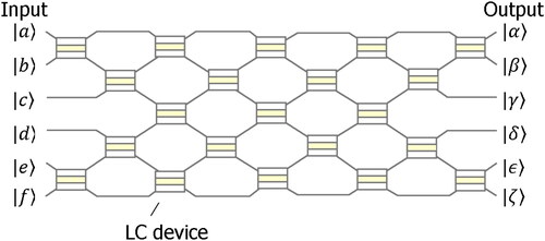
There is a lot of research being done on quantum computing [Citation1–25]. In 2019, Google reportedly achieved quantum supremacy [Citation1], and in 2021, IBM unveiled a 127-qubit quantum processor [Citation2] Google’s quantum computers use quantum annealing in the transverse Ising model [Citation3–5]. On the other hand, IBM’s quantum processor uses a gate system with cryogenic superconducting elements [Citation6–11]. Other methods have been reported, including ion traps [Citation12–16], quantum dots [Citation17, Citation18], Diamond NV centers [Citation19–21], and gating methods using a photon-quantum system [Citation22–25], Among these methods, the photon-quantum system is fascinating because it requires no cooling apparatus, is highly resistant to external disturbances, and has a long coherence time of around one ms. We have started research on optical quantum computing technology using organic devices, and have started basic experiments using the optical phase control of liquid crystal (LC) devices [Citation26]. Here, the response time of the LC device is relatively slow as ms order. However, if the LC device creates an arbitrary configuration of the photon-quantum system as Pauli-gate, Hadamard-gate, and controlled-NOT gate by applying an appropriate voltage, this quantum circuit operates at a frequency range of light (∼1014 Hz). Therefore, the LC device acts as a software computer, i.e., an active-type photon universal computing (APU) which we think will be realized, as shown in . At this time, we review recent research in various types of our optical quantum computing using liquid crystal devices. First, we focus on basic research of Young’s interference experiment. The light emitted from the light source is directed toward the screen at a short distance from the divided slit. In the case of light from a single light source, the light intensity in front of the light source on the screen is the maximum, and the intensity decreases as the light source shifts away from the center of the light source. When the light is divided by two slits, the light intensity in front of the light source, which should not be irradiated, is maximized, and the light is weakened or strengthened according to the optical path difference, resulting in a change in intensity. At this time, we have investigated Young’s interference experiment using a self-aligned LC optical control device with a nematic LC cell composed of two divided directional controls of the alignment layer. By applying the voltage, the change of the interference pattern under laser irradiation was evaluated. Second, we report on a simulation of the phase control of two-photon paths between the reference state and incoming state of the LC device under applied voltage control, aiming to realize a quantum computer that can be freely configured with universal photon quantum circuits. Third, a TN LC device is inserted into one path in a Mach–Zehnder interferometer, which divides one light source into two paths with a beam splitter, to control the interference state of weak quantum light. During this situation, there are many reports of the optical phase control using Mach–Zehnder interferometer and TN LCs [Citation27]. However, the trials of this study were confirmed by the change in light intensity at very weak photon count levels of the order of 1,000 count/s or less. We report on the observation of changes in the optical interference state and changes in the number of photons in the weak light intensity [Citation28–38]. Fourth, we focused on single-photon, linear optical device quantum calculators using linear optical devices and the Deutsch-Jozsa algorithm [Citation39], and we thought that by using an LC device for the optical phase control part of this method, we could create an optical quantum bit calculator. Therefore, as an initial study for the realization of a future linear optical quantum computer, we conducted basic experiments on 2-bit quantum computation related to the Deutsch-Jozsa algorithm. In detail, we have reported on the variation of the optical intensity of the output interference light concerning the voltage input and the photon number to the input logic state in the weak light condition.
Figure 1. Concept of active-type photonic universal computing (APU).
2. Comparison of classical optical computing and quantum computing [Citation26]
Optical computing uses the switching and interference effects of light to perform operations with light. On the other hand, quantum computing, also known as photon computing, uses light in the quantum entanglement state of photons to perform operations. Orthogonal polarization states can be used as qubits. The state is obtained as an expected value at the final measurement state. If a measurement is made in the middle of a path, the state does not show a quantum state, and the state is obtained as if it was a classical computing operation. In addition, let us consider another case. For example, the decoherence length of a photon is around 1 ms, during which time the light travels 300 km in a vacuum. At a distance of less than 300 km, there is only one photon in the optical path L (less than 1,000 count/s (cps)). For example, Young’s two-slit experiment has confirmed that the same result as the interference state occurs in this single-photon state. In this case, the inequality for the average running length Lp of a single photon when a single photon passes through in the optical path is as
(1)
(1)
where c is the speed of light and Np is the number of incident photons during 1 s. When this relation is satisfied, a single-photon state is obtained on average in the optical measurement system, i.e., the photonic quantum effect due to a single-photon is carried out in the system.
3. Young’s interference experiment using self-aligned liquid crystal optical control devices [Citation26]
3.1. Overview of Young’s interference experiment to control the optical phase of LCs
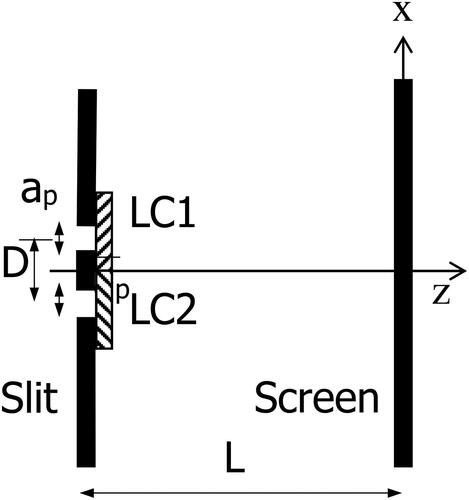
shows an overview of the experimental system of Young’s interference experiment using an LC phase control device in this study. Light generated from a single light source is divided by a slit in order to induce the interference. The light is then introduced into an optical phase-controlled LC device with an alignment region that is divided into two regions, and interference patterns are independently controlled. In the LC directors in the figure, the orientation of the director is assumed to be twisted nematic alignment. Considering the next application of optical quantum devices, it will be desired that the polarization states of the two directors are set to be orthogonal based on the Hilbert space theory. For this reason, the orientation direction of the LC in the two domains was initially set to π/2 for the initial incident light. Subsequently, a diffraction pattern of output light is generated on the screen provided through a certain distance. In the double-slit experiment, for example, the output light is into the LC, the phase in the two domains changes, and the interference pattern of the output light is changed.
Figure 2. Overview of experimental system of Young’s interference experiment using LC phase control device. Light generated from single light source is divided by slit and is introduced into optical phase-controlled LC device [Citation26] (©2023 Liq. Cryst.).
![Figure 2. Overview of experimental system of Young’s interference experiment using LC phase control device. Light generated from single light source is divided by slit and is introduced into optical phase-controlled LC device [Citation26] (©2023 Liq. Cryst.).](/cms/asset/a4f3ef8b-1e14-4ed8-bd98-cfdf75b5bf86/gmcl_a_2342610_f0002_b.jpg)
3.2. Simulation method
shows the optical configuration with double slits. The configuration can be changed into two regions after passing through the slits. First, the light intensity on the screen in the unchanged case is given by the Fraunhofer approximation by the following equation [Citation40,Citation41],
(2)
(2)
where
is the wavelength of the incident light,
is the distance between the two slits (slit separation),
is the aperture length of the slit,
is the distance between the slit and the screen,
is the distance from the center on the screen,
and maximum intensity is
Figure 3. Optical configuration with double slits. The configuration can be changed into two regions after passing through the slits. is distance between two slits,
is aperture length of slit,
is distance between slit and screen,
is distance from center on screen (©2023 Liq. Cryst.).
In the simulation, the light intensity and its change on the screen from the center of screen were calculated. The LC region was placed tangential to the slit, and simulations were made for cases where the phase difference of the light in the two regions was in-phase and for cases where the phase difference was changed by The light source was assumed to be a He-Ne laser with a wavelength of
and
3.3. Process and experimental methods of LC device with self-aligned electrode structure
A -wide single line pattern was fabricated by photolithographic patterning of the initially deposited electrodes of Ta or Cr (evaporation or sputtering) in order to avoid the influence of diffracted light intensity due to changes in various parameters, the diffraction pattern was evaluated with two domain regions formed by a simple wider aperture length of the slit. The device fabrication process is shown in . Here, in order to reduce stray light, we applied a self-alignment structure in which the distance between the slit and the LC is kept close to the ideal limit of sub-micron [Citation42]. shows the difference in optical configuration between the control device studied before the starting of this research work and the self-aligned optical phase control LC device. In the optical arrangement of the previous device, the light after slit incidence propagates through the 0.7 mm glass and reaches the two divided LC sections (upper in ). Therefore, at the previous research work of incidence into the LC, some of the incident lights after passing through the slit crossed each other, resulting in a lot of stray light. As a result, the difference in diffraction intensity due to the phase change became indistinguishable. In contrast, the self-aligning structure not only minimizes the distance between the slit and the LC, but also minimizes the distance between the electrode and the slit, providing the ultimate alignment condition. The slit of Ta or Cr was formed on the substrate by sputtering or electron beam evaporation apparatus, and patterning of 25 µm-wide single line are formed. Subsequently, SiO2 and Indium-Zinc-Oxide (IZO) were sputter-deposited. Nega-type photoresist (AZ-CTP100, Clariant) was then spin-coated and exposed after pre-baking (). After development process, a pattern was formed in which the slit electrode and photoresist were self-aligned (). The IZO was etched using this pattern, and patterning was done in two parts of the electrode (). After removing the photoresist (), a SiO2 insulating layer and Cr were sputtered to reduce uncontrolled light and form apertures, which cannot be shown in the figure due to its dimension. As a result, aperture area of 4 × 1 mm was formed. As the LC alignment film, 60° oblique evaporation technique was used [Citation43]. For division of orientation [Citation44], the orientation film formation area was pattern segmented by photoresist as shown in to orient the film with an orientational difference of 90° (). The other substrate is coated with indium tin oxide (ITO) electrodes, and the two substrates are bonded so that the orientation direction is ±45°, symmetrical and twisted in the opposite direction. The operation of the LC cell is like that of a typical reflective display, the 45-degree TN mode [Citation45] with good polarization conversion and faster switching speed. The ITO Substrates with 60° oblique evaporation alignment are then bonded together via 6 µm diameter ball spacers, and finally the LC material (LIXON-5049-XX, JNC, Δε = 5.1, Δn = 0.100, N(101 °C) Iso) was injected and sealed to complete the cell, as shown in the upper figure of . The oblique evaporation directions for the top and bottom substrates of the LC cell are described in the lower figure of . The evaporation direction on the upper substrate was a π/2 rotated direction.
Figure 4. Device fabrication process under study. Here, self-alignment structure is formed in which the distance between slit and LC is kept close to ideal limit [Citation26] (©2023 Liq. Cryst.).
![Figure 4. Device fabrication process under study. Here, self-alignment structure is formed in which the distance between slit and LC is kept close to ideal limit [Citation26] (©2023 Liq. Cryst.).](/cms/asset/1072e381-a91f-48ab-b129-e80c5285fffb/gmcl_a_2342610_f0004_b.jpg)
Figure 5. Difference in optical configuration between control device studied before starting of this research work and self-aligned optical phase control LC device [Citation26] (©2023 Liq. Cryst.).
![Figure 5. Difference in optical configuration between control device studied before starting of this research work and self-aligned optical phase control LC device [Citation26] (©2023 Liq. Cryst.).](/cms/asset/0b631c3d-5e09-403f-859b-5aa7111eafbc/gmcl_a_2342610_f0005_b.jpg)
Figure 6. Oblique evaporation method with divided two different alignment regions. Orientation film formation area was pattern segmented by photoresist (©2023 Liq. Cryst.).
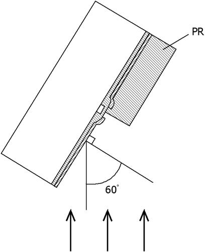
Figure 7. Complete fabrication of cell structure. Upper figure shows exterior appearance of LC cell and lower figure shows oblique evaporation directions for top and bottom substrates of LC cell [Citation26] (©2023 Liq. Cryst.).
![Figure 7. Complete fabrication of cell structure. Upper figure shows exterior appearance of LC cell and lower figure shows oblique evaporation directions for top and bottom substrates of LC cell [Citation26] (©2023 Liq. Cryst.).](/cms/asset/bf998a55-b9d3-45d8-a2b7-e01e6cd963c6/gmcl_a_2342610_f0007_b.jpg)
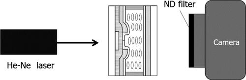
To confirm the threshold voltage and operating behavior of the LC cell, the voltage-transmittance (Tr-V) characteristics were checked under a polarization microscope. Next, Young’s interference experiment was carried out using the measurement system, as shown in . In this measurement, the fabricated LC device was irradiated with He-Ne laser light (wavelength of 632.8 nm) at the center of the slit, and the diffraction pattern of the light after passing through the LC device was changed. The amplitude of the voltage was varied. The outgoing light was directly captured with a single-lens reflex camera with a neutral density (ND) filter. The image data was converted to 8-bit gray level and analyzation was carried out. Here, the number of horizontal axes is corresponding to the position of the pixel in camera data.
Figure 8. Measurement system of Young’s interference experiment. Light source under study is He-Ne laser light at wavelength of 632.8 nm. LC cell placed at center of slit and diffraction pattern of light after passing through LC device was measured using single-lens reflex camera with neutral density (ND) filter (©2023 Liq. Cryst.).
3.4. Simulation result
As a preparatory step for conducting the experiment, a simulation analysis of the optical phase control LC device was performed, as shown in . The horizontal axis was normalized using the value to clarify the peak position by phase change. The solid line compares the case with no phase shift due to the LC region in , and the dotted line compares the case with a two-slit phase control device, where the phase difference at both slits is zero and
respectively, i.e., this corresponds to the voltage application state. Comparing the two cases, the analysis with a phase difference o shows that in the region of
the contribution of the Sinc function to the change in light intensity is large and the light intensity between the two lines is inverted. In the region where
or higher, the peak intensity is small, however, the light intensity changes due to trigonometric function changes were observed. The former is due to the contribution of the distance
between the slits, which makes the central area darker, and the latter is due to the aperture length
of the slits. In the absence of phase shift due to the liquid crystal element, as in the case of the usual two-slit case, a peak was produced at the center, which was shadowed by the effect of interference and took the maximum value. In the results with a phase shift of
the period of the intensity of the Sinc function was nicely reversed, and the intensity decreased as one moved away from the center while the peaks and valleys of the peaks were also reversed.
Figure 9. Simulation result of Young’s interference experiment of optical phase control LC device. Horizontal axis was normalized using value and vertical axis show intensity of outgoing light [Citation26] (©2023 Liq. Cryst.).
![Figure 9. Simulation result of Young’s interference experiment of optical phase control LC device. Horizontal axis was normalized using value ξ=xap/λL and vertical axis show intensity of outgoing light [Citation26] (©2023 Liq. Cryst.).](/cms/asset/b9f9883f-a4f9-4aaa-a0d2-d0df526919b3/gmcl_a_2342610_f0009_b.jpg)
3.5. Experimental results and discussions
shows transmittance-voltage (Tr-V) characteristics at one of the LC regions under the polarization microscope. Filled circles and open circles are the cases of under parallel Nicols and crossed Nicols, respectively. The threshold voltage is 1.3 V. Due to the angle between the polarizer and the alignment direction of LCs, the transmittance at V = 0 is 0.624 times the maximum value of transmittance under crossed polarizer. By applying the voltage above 1.3 V, the transmittance was once increased and reached a maximum value at V = 1.8 V and was gradually decreased to increase the voltage under the crossed Nicols. On the other hand, the Tr-V curves are symmetrical concerning the half value of maximum transmittance between parallel and crossed Nicols.
Figure 10. Transmittance vs voltage characteristics at one of LC region under polarization microscope. Filled circles and open circles are case of under parallel nicols and crossed nicols, respectively [Citation26] (©2023 Liq. Cryst.).
![Figure 10. Transmittance vs voltage characteristics at one of LC region under polarization microscope. Filled circles and open circles are case of under parallel nicols and crossed nicols, respectively [Citation26] (©2023 Liq. Cryst.).](/cms/asset/08062076-cbf6-4fe3-aa4b-daae6eddc974/gmcl_a_2342610_f0010_b.jpg)
shows a photograph of the interference fringes pattern, where (a) is 0 V, (b) is 2 V, (c) is 2.5 V, (d) is 3 V, (e) is 4 V, and (f) is 9 V condition. The change of interference fringes pattern started at around 1.5 V, and a fine diffraction pattern appeared above 2 V. At higher voltages, the diffraction pattern became more gradual. At 9 V, the patterns of bright and dark lines were interchanged compared to those at 2 V.
Figure 11. Photograph of interference fringes patterns, where (a) is 0 V, (b) is 2 V, (c) is 2.5 V, (d) is 3 V, (e) is 4 V, and (f) is 9 V condition [Citation26] (©2023 Liq. Cryst.).
![Figure 11. Photograph of interference fringes patterns, where (a) is 0 V, (b) is 2 V, (c) is 2.5 V, (d) is 3 V, (e) is 4 V, and (f) is 9 V condition [Citation26] (©2023 Liq. Cryst.).](/cms/asset/bf952975-901f-40aa-9cfb-1d1dc15b70d8/gmcl_a_2342610_f0011_b.jpg)
In order to analyze precisely, the intensity of the interference pattern was converted to an 8-bit gray level at the horizontal line to the extended direction of the interference pattern, as shown in . The applied voltages were 0, 2.5, and at 9 V, where dotted line, gray line, and solid line, respectively. The interference pattern at 0 V, the pattern was overlapped in the case of 9 V. The light intensity was a superimposed pattern of Sinc functions and fine oscillations. When the voltage was applied, the light intensity gradually changed to be dominated by the Sinc function, which changed greatly, and the peak position at 0 V became minimal.
Figure 12. Typical interference pattern with converted to eight-bit gray level at the horizontal line [Citation26] (©2023 Liq. Cryst.).
![Figure 12. Typical interference pattern with converted to eight-bit gray level at the horizontal line [Citation26] (©2023 Liq. Cryst.).](/cms/asset/6da9623a-ab5d-4301-b58c-ef9495c6bf18/gmcl_a_2342610_f0012_b.jpg)
shows a graph of light intensity without and with voltage application of 2.5 and 9.0 V. Points A and B correspond to the distance value at −1,297 and −1.034, respectively. The logic values of “0” and “1” at points A and B were clearly switched between 0 V and 2.5 V, and between 2.5 V and 9 V. The maximum difference in light intensity between 0 V and 2.5 V was 3.0. From this situation, clear “NOT” logic of light intensity could be observed at point B by applying the voltage between 0 and 2.5 V, in addition, to between 2.5 and 9 V. On the other hand, in point A, these operations are a little small, however, a small difference of inversion in light intensity is observed between 2.5 and 9.0 V. At this moment, due to the distance of the glass thickness between the LC and the slit, stray light also occurred, and only minute changes in interference fringes could be obtained.
Figure 13. Logic operation of position a and b for "0" and "1" points. Applied voltages are among 0, 2.5 and 9 V. Where point A and B corresponds to distance value at −1,297 and −1,034, respectively [Citation26] (©2023 Liq. Cryst.).
![Figure 13. Logic operation of position a and b for "0" and "1" points. Applied voltages are among 0, 2.5 and 9 V. Where point A and B corresponds to distance value at −1,297 and −1,034, respectively [Citation26] (©2023 Liq. Cryst.).](/cms/asset/62aaa03b-a557-4ec4-9cf9-f77b3eb3ff52/gmcl_a_2342610_f0013_c.jpg)
Finally, the period of both light intensity changes is then briefly discussed. One period of the Sinc function is determined by the width of the electrode at the center, which is the shadow area of the incident light. The peak of the fine period is determined by the width of the apertures formed at both ends of the shadow slit. A detailed check of the period width revealed a difference of 14.5 times for the period. This value is nicely explained by the central shadow slit width and aperture and
In this context, the self-alignment of the electrode structure reduced stray light in the substrate and allowed us to confirm a clear change of “0” and “1” at points A and B. In the future, by decreasing the aperture width
compared to
and reducing the contribution of light intensity to the trigonometric distribution, it should be possible to obtain clearer logic values. In addition, we will continue our research using micro-quantum light to reduce stray light such as interfacial reflections.
4. Numerical quantization of interfering photons using liquid crystal retarder [Citation46]
4.1. Calculation of beam splitter operation
In this Section, we report on a simulation of the phase control of two-photon paths between the reference state and incoming state of the LC device under applied voltage control, aiming to realize a quantum computer that can be freely configured with universal photon quantum circuits.
Before starting a calculation, consideration of a beam splitter and a phase shifter are expressed, as shown in . The beam splitter is a four-port device with the relation in the Heisenberg picture [Citation47],
(3)
(3)
where
(i = 1, 2) is the creation and annihilation operator, respectively. The matrix U(2) is expressed as
(4)
(4)
where a common beam splitter can be expressed by phase shift δ, δ’, and ϕ, and linear combination of reflectivity and transmittance parameters using square root of -sinθ and cosθ, respectively.
Figure 14. Optical configuration of a beam splitter with the input-output relations in the Heisenberg picture. The beam splitter used is a liquid crystal retarder under study [Citation46] (©2024 JJAP).
![Figure 14. Optical configuration of a beam splitter with the input-output relations in the Heisenberg picture. The beam splitter used is a liquid crystal retarder under study [Citation46] (©2024 JJAP).](/cms/asset/4783a325-f2ba-4934-bd7c-667da24305b7/gmcl_a_2342610_f0014_c.jpg)
We consider the phase shift in one of the annihilation operators using the LC device. In this calculation, the amplitude of these operators is ultimately reduced during the below calculation. As a result, a quantization condition of photons with small amplitude can be calculated.
4.2. Calculation of liquid crystal retarder
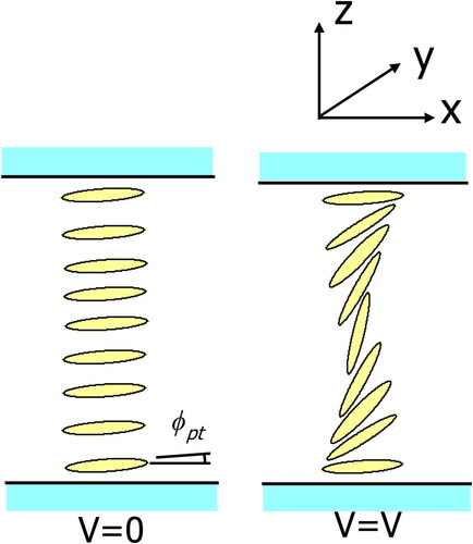
We consider the phase shift of the coherent state by changing the applied voltage in the LC device. shows an image of an LC director configuration. The device considered was a homogeneous alignment, and the director profile and the resultant phase change by the applied voltage were computationally analyzed.
Figure 15. Image of liquid crystal director configuration. Where the initial condition of the LC director at z = 0 and z = d is tilted to a pretilt angle, the electric field is applied to the z direction. Under voltage application above threshold voltage Vth, director deformation has occurred (©2024 JJAP).
First, we would consider a profile of director n using Frank’s free energy equation as [Citation48]
(5)
(5)
where K11, K22, and K33 is the splay, twist and bend elastic constant, respectively, geometric arrangement of
and electric field of
are considered.
By calculating these conditions, free energy of elastic deformation can be calculated into above equation and simplified to the Euler-Lagrange equation calculated as [Citation49]
(6)
(6)
where Δε is the dielectric anisotropy.
In the Euler-Lagrange Equation, is fixed to
at
and
where
is the cell thickness. By assuming the symmetry,
Here,
at
[Citation50],
(7)
(7)
This equation is transformed using equation as
(8)
(8)
We consider the limitation as a threshold electric field is calculated as
(9)
(9)
Strictly speaking, for the Fredericks transition, Ec is obtained by ϕpt approaches zero. Note that in the range of ϕpt about less than 1 degree, the behavior occurs in electric fields below Ec. In such a range, ϕpt is considered to define the direction of LC director. Above threshold condition, the director profile at arbitrary point is estimated below equation
(10)
(10)
(11)
(11)
where
In some cases, it is easier to calculate the differential form, therefore I describe the following equation as,
(12)
(12)
By using these equations, we can calculate the director profile of LC medium through the LC cell.
In the director profile calculation, the following procedure and parameters are used. The calculation program used is Visual Basic 2010 (Microsoft), double-precision, floating-point number. In the calculation, the director profile during the LC cell is divided into 1,000. In order to calculate the differential equation analysis, the Runge-Kutta-Gill method was used for the director calculation. The dielectric anisotropy of LC Δε = 5, refractive index anisotropy Δn = 0.100, and the splay and bend elastic constant is K11 = 10 pN and K33 = 15 pN, respectively. Using EquationEq. (12)(12)
(12) , the estimated threshold voltage VC = EC ×d = 1.75 V.
4.3. Setting of Hamiltonian and eigenvalue of energy
One of the fundamental Hamiltonian is expressed using the creation and annihilation operators as [Citation51]
(13)
(13)
This expression is the total energy of the electromagnetic wave in a vacuum. Here, where
is the photon number operator for a state with n photons of frequency ω. In this case, the Hamiltonian is
(14)
(14)
The eigenvalue of energy at state is
(15)
(15)
shows the eigenvalue of energy at state as expressed in EquationEq. (15)
(15)
(15) . The energy state, i.e., photon number operator, has a discrete value, and the creation and annihilation operator act as
and
respectively. In particular, even in the absence of a single photon, there remains an energy of
per mode, known as the zero-point energy. Here, it is assumed that the wavelength of incident light is 632.8 nm.
Figure 16. Image of Hamiltonian and eigenvalue of energy at state Photon number of operator
is introduced [Citation46] (©2024 JJAP).
![Figure 16. Image of Hamiltonian and eigenvalue of energy at state |n. Photon number of operator n̂, n̂=â†â is introduced [Citation46] (©2024 JJAP).](/cms/asset/1a32eb37-007d-4ced-9152-7b11494fc59a/gmcl_a_2342610_f0016_b.jpg)
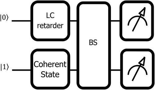
4.4. Calculation of quantum circuit form for linear optics of beam splitter
In order to treat the calculation, a quantum circuit form for linear optics of the beam splitter is employed, as shown in . For the initial state, two input states of and
are introduced into the LC retarder and coherent state. Then two beams are entangled into the linear optics of the beam splitter. The programming software used is Python 3.9, libraries used are NumPy, matplotlib, and Decimal.
Figure 17. Quantum circuit form for linear optics of beam splitter (©2024 JJAP).
4.5. Simulation results of LC director profile and retardation
The calculated director profile is shown in . Vertical axis is the polar angle between the substrate plane and the long axis of the LC molecule, i.e., this angle is identical to the tilt angle. The horizontal axis is the normalized distance z/d, where the position of thickness is z and normalized by the cell thickness d. The calculated voltage conditions are 2, 4, 6, 8, and 10 V. By increasing the voltage, the maximum polar angle at the middle of the cell gradually approaches Sometimes, in this type of calculation, the discontinuity point at the center of the cell was observed. However, due to precise calculation, a clear and continuous polar angle curve could be obtained.
Figure 18. Calculated director deformation under voltage application. The applied voltage is 2, 4, 6, 8, and 10 V where the division number of liquid crystal cells is 1,000 [Citation46] (©2024 JJAP).
![Figure 18. Calculated director deformation under voltage application. The applied voltage is 2, 4, 6, 8, and 10 V where the division number of liquid crystal cells is 1,000 [Citation46] (©2024 JJAP).](/cms/asset/87009493-746d-420d-8b54-b3c4b539c6c3/gmcl_a_2342610_f0018_b.jpg)
shows the calculation result of retardation. The value of retardation variation is considered, where the retardation value below the threshold voltage of 1.75 V is set at zero and is evaluated. By increasing the voltage, the polar angle of the director profile at the middle of the LC cell approaches
and the amount of retardation change was gradually decreased. However, total retardation change is reached above 1.2. The change in this value implies a large phase change of more than π rotation. There, full control of the retardation could be achieved under an evaluation situation.
Figure 19. Calculation result of retardation by changing voltage. The vertical axis is retardation variation where n is the actual refractive index, d is cell thickness and λ is the wavelength of light. Insets of the figure are director profiles at voltages of 2, 4, 6, and 8 V [Citation46] (©2024 JJAP).
![Figure 19. Calculation result of retardation by changing voltage. The vertical axis is retardation variation nd/λ, where n is the actual refractive index, d is cell thickness and λ is the wavelength of light. Insets of the figure are director profiles at voltages of 2, 4, 6, and 8 V [Citation46] (©2024 JJAP).](/cms/asset/c95d5785-c1d7-4d76-bb98-2cc9fb322b24/gmcl_a_2342610_f0019_b.jpg)
4.6. Simulation results of intensity vs. voltage characteristics
Before considering the evaluation of the intensity (Int) vs. voltage (V) characteristics in a quantum case, a classical case with the amplitude αI of unity is evaluated. shows the Int-V characteristics in the classical case. The Int-V characteristics show a constant below the threshold voltage of 1.75 V. By increasing the voltage, the intensity was changed rapidly. The voltage above 4 V, the intensity was saturated and few changes were observed.
Figure 20. Intensity vs. voltage characteristics for the classical case, amplitude α1 = 1 [Citation46] (©2024 JJAP).
![Figure 20. Intensity vs. voltage characteristics for the classical case, amplitude α1 = 1 [Citation46] (©2024 JJAP).](/cms/asset/e8b9aaa8-b2cd-4b7e-a24a-d240dcfd33d6/gmcl_a_2342610_f0020_b.jpg)
The calculation results of Int-V characteristics for the quantum case are shown in at an amplitude of intensity αI equals 6.3 × 10⁻¹⁰. Discontinuous quantization of photon was calculated by the application of voltage above the threshold voltage of 1.75 V. However, sometimes, the intensity is asymmetry changed to the mid of vertical value. This is due to the small retardation change-induced creation and annihilation operators. In other words, it can be said that asymmetry is caused by fluctuations due to the uncertainty principle. By reducing the number of photons to αI = 2.6 × 10⁻¹⁰, tri-state and symmetrical digital change of intensity was obtained, as shown in . By further reducing the amplitude, in other words, without the photon case, the value of zero-point fluctuation half of ℏ𝜔 can be seen, as shown in . Therefore, both of the operators and
show the same energy value of 2.50 × 10⁻²⁰ J. Numerical validation and experimental demonstration are our future subject.
Figure 21. Intensity vs voltage characteristics for amplitude of intensity α1 = 6.3 × 10⁻¹⁰ [Citation46] (©2024 JJAP).
![Figure 21. Intensity vs voltage characteristics for amplitude of intensity α1 = 6.3 × 10⁻¹⁰ [Citation46] (©2024 JJAP).](/cms/asset/acdb99cf-1f26-44e7-8a55-ccc30ab091a9/gmcl_a_2342610_f0021_b.jpg)
Figure 22. Intensity vs voltage characteristics for amplitude of intensity α1 = 2.6 × 10⁻¹⁰ [Citation46] (©2024 JJAP).
![Figure 22. Intensity vs voltage characteristics for amplitude of intensity α1 = 2.6 × 10⁻¹⁰ [Citation46] (©2024 JJAP).](/cms/asset/cdca5b42-aae6-4cbf-aba2-57f95c1c242c/gmcl_a_2342610_f0022_b.jpg)
Figure 23. Intensity vs voltage characteristics for amplitude of intensity α1 = 2.0 × 10⁻¹⁰ [Citation46] (©2024 JJAP).
![Figure 23. Intensity vs voltage characteristics for amplitude of intensity α1 = 2.0 × 10⁻¹⁰ [Citation46] (©2024 JJAP).](/cms/asset/1f6e05dd-9d1e-4d63-bd3f-76e780a6c57e/gmcl_a_2342610_f0023_b.jpg)
5. Quantum optical control experiment using Mach–Zehnder interferometer and twisted nematic liquid crystals [Citation38]
5.1. Backgrounds of the four-port optical control experiment
A classical computer performs logic operations on classical bits represented by binary values of 0 and 1, which are the minimum units of information. Quantum computers, on the other hand, perform logical operations on qubits, whose information is represented by a superposition of 0 and 1. The qubit state vector is expressed as using the probability amplitudes α and β, and the sum of the squares corresponds to the probability of measuring 0 or 1. Therefore, it is normalized to a total of 1, such as
A single photon has very convenient properties for this qubit. The polarization state vector of a photon is represented by
for horizontal polarization
vertical polarization
using the polarization angle θ and phase angle ϕ. Here,
and
can be set as the probability amplitudes of horizontal and vertical polarization, and the sum of their squares is 1. As analogous to this, the polarization state vector of a photon is displayed as an arbitrary Bloch spherical point. In other words, the vertical and horizontal polarization states of a single photon can be used to define a polarization quantum bit. Given the above light and phase controllability, there exists interest in optical quantum computing using quantum bits of optical phase control technology using LC devices. The LC devices can significantly change the polarization, phase, and rotation state of light by applying a voltage of only a few volts. Taking advantage of the characteristics of this LC device, we would like to show the possibility of optical logic operations that can represent 0 and one of polarization qubits by utilizing the characteristics that greatly convert the polarization state of TN liquid crystals and the interference optical system [Citation26].
The features of this study are quantum light control using an LC device. A TN LC device is inserted into one path in a Mach–Zehnder interferometer, which divides one light source into two paths with a beam splitter, to control the interference state of weak quantum light. During this situation, there are many reports of the optical phase control using Mach–Zehnder interferometer and TN LCs [Citation27]. However, the trials of this study was confirmed by the change in light intensity at very weak photon count levels of the order of 1,000 count/s or less. We report on the observation of changes in the optical interference state and changes in the number of photons in the weak light intensity.
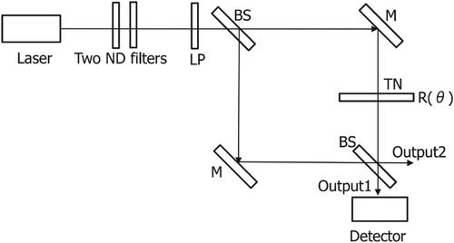
5.2. Experimental setup using Mach–Zehnder interferometer and twisted nematic liquid crystals
The experimental system is shown in . The light source used was a randomly polarized He-Ne laser, and a linear polarizer (LP) was installed before the laser beam irradiation to light pass in the horizontal polarization direction. The specification of the He-Ne laser is 7 mW with a wavelength of 632.8 nm. Using these conditions, the number of photons of the light source can be calculated as (counts/s). For the weak light measurement, two neutral density (ND) filters (transmittance =
) were used to obtain the weaker intensity of the laser light. We were able to do measurements using weak light by creating a darkroom environment.
Figure 24. Optical experiment system under study. Laser: He-Ne Laser (632.8 nm); BS: Beam splitter; M: Mirror; TN: Twisted Nematic LC (©2024 JJAP).
In the present work, we focus only on the polarization change of the TN LC and briefly present the electric field intensity calculation using the rotation matrix of the Jones’ matrix. For simplicity, the z-axis direction of the propagation light state is assumed to be uniform.
(16)
(16)
where
are the phase states of the electric fields, respectively.28)
The after passing through the TN LC device is simply shown below using the rotation matrix
since we are only focused on the polarization changes due to the TN LC.
(17)
(17)
The output light intensity I is shown below,
(18)
(18)
The interference state in the light intensity depends on the of the optical rotation. The results of the interferometric intensity simulation at this output light are shown in . The two outputs of the Mach–Zehnder interferometer behave differently. The open circle and solid circle represent the intensity changes of the two outputs of the interferometer when the polarization is changed. In addition, was calculated using EquationEq. 18
(18)
(18) .
Figure 25. Simulation results of interference light intensity [Citation38] (©2024 JJAP).
![Figure 25. Simulation results of interference light intensity [Citation38] (©2024 JJAP).](/cms/asset/e4419112-9077-4ffd-b107-69dfd95b6f00/gmcl_a_2342610_f0025_b.jpg)
The interference fringes spacing d can be controlled by using
in and the wavelength of laser light
Using the image of at 5 V, when the beam length was set to 1.5 mm, the d measured using image analysis software was 59 μm. Since the λ is 632.8 nm, and
from the above formula.
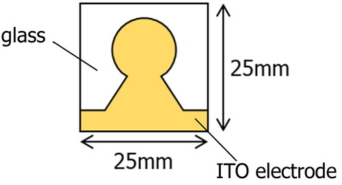
Next, the fabrication process of TN LCs, as shown in , and their voltage transmittance characteristics are described. The glass substrate was coated with ITO with a thickness of 30 nm. The glass substrates with ITO electrodes (hereinafter referred to as “ITO substrates”) were cut into 25 mm × 25 mm square pieces, patterns were formed using masks and photoresists, and excess ITO electrodes were etched using ITO etchant (hydrochloric acid: nitric acid: deionized water = 1: 2: 3) to form electrodes patterning. In order to remove unnecessary ITO from this patterned glass substrate, etching with ITO etching solution is carried out. The shape of the ITO pattern is shown in . After the substrate was cleaned, polyacrylonitrile (PAN) was coated as an alignment film, and the rubbing direction of the upper and lower substrates was rotated 90° and the rubbing process was carried out.
Figure 26. Configuration of TN liquid crystal cell.
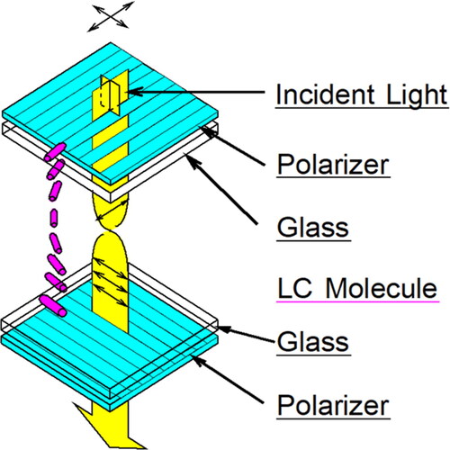
Figure 27. Shape of ITO pattern after ITO electrodes were etched (©2024 JJAP).
To control the cell thickness uniformly, a spacer with a diameter of 6 μm was mixed into the epoxy adhesive and coated around the peripheral of the LC cell. The LC used was LIXON-5049XX (JNC,
).
Voltage vs transmittance characteristics of the fabricated TN LC cells were measured using a polarization microscope. shows the voltage vs transmittance characteristics of the obtained TN LC cell. The graph shows that the threshold voltage is 2.0 V. At higher voltages, the transmittance changes steeply at first and then gradually as the voltage is increased. Obtained maximum contrast ratio was 198: 1.
Figure 28. Voltage vs transmittance of TN LC device under study [Citation38] (©2024 JJAP).
![Figure 28. Voltage vs transmittance of TN LC device under study [Citation38] (©2024 JJAP).](/cms/asset/b4da7fda-86d0-4d34-879d-78ccb97035fa/gmcl_a_2342610_f0028_b.jpg)
5.3. Experimental results and discussions
shows the pattern change of the interference light. At a voltage of 1 V, the polarization of the two laser beams was 90° different and no interference occurred. At a voltage of 2 V or higher, the polarization of the laser beam passing through the TN LC device gradually changed and interference patterns appeared. A bright ring is visible in the image, which is due to the interference between two laser beams. Comparing the interference light images when a voltage of 3 V is applied and the interference fringes have shifted at the voltage of 5 V. This is due to the phase shift of the light by the TN LC devices. In this way, the polarization state could be converted by the TN LC device to obtain a change of state as a polarization quantum bit.
Figure 29. Change in the pattern of interfering light due to the application of voltage to the LC device [Citation29] (©2024 JJAP).
![Figure 29. Change in the pattern of interfering light due to the application of voltage to the LC device [Citation29] (©2024 JJAP).](/cms/asset/e9553d5b-9e5a-4dbb-9fac-d7d469daedab/gmcl_a_2342610_f0029_b.jpg)
Next, we will discuss the results of the weak light measurement. The results of photon counting measurements in weak light conditions are shown in . The average value was calculated by subtracting 0.66 counts of the average dark count over a 10 s period, from the measurement at each voltage. In a similar to the interference light pattern observation results, as the voltage was increased from 1 V, the change of interference condition began to occur and the photon counts dropped and saturated at 0.77 counts at 5 V.
Figure 30. Number of photons vs voltage characteristics [Citation38] (©2024 JJAP).
![Figure 30. Number of photons vs voltage characteristics [Citation38] (©2024 JJAP).](/cms/asset/f37753ea-0c99-4c2b-8074-dc24a4b46fa8/gmcl_a_2342610_f0030_b.jpg)
The results of photon counting measurements for weak light states will be discussed. Photons have confirmed the wave-particle duality of the light according to quantum optics. And this cannot be measured at the same time. First, at a voltage of 1 V, the polarization states of the two beams in the Mach–Zehnder interferometer are different, indicating the particle nature of the photons. As the voltage gradually increased, the polarization states of the two beams were gradually matched, and the wave nature of the photons exhibited a completely interference state at 5 V. The voltage vs transmittance characteristics show that the polarization of light passing through the TN LC device is sharply twisted by nearly 90° at 2 ∼ 2.5 V. However, the photon count measurement results for the weak light state do not obtain a similar tendency to the voltage vs transmission characteristics. As mentioned in the result, the interference light image in shows not only the polarization state but also the phase state changes, as indicated by the result that the interference fringes are inverted between 3 V and 5 V. This is because that the light intensity calculation derived in Section 5.2 will change not only the deflection angle but also the phase angle
as
(19)
(19)
From the above equation, we have to consider the changes between and are different light states. The phase change can be considered to be due to a change in retardation caused by a change in LC orientation. The phase difference of the LC is expressed as where
is the birefringence index,
is the cell thickness, and
is the wavelength. From this relation, if we would like to suppress the phase change, the cell thickness should be reduced [Citation52, Citation53].
Next, we consider the interference state. Originally, we had to match the phase difference and eliminate interference light. As can be seen from EquationEq. (18)(18)
(18) , if the phase difference is set to zero, one of the two output lights will be intensified and the other light intensity will be completely weakened. However, the interference light did appear even when the phase difference was eliminated. There are two reasons for this phenomenon. First, light is not completely split in two ways by the input beam splitter. Second, the above calculation process assumes perfectly coherent light, however, the laser light used in this experiment is Gaussian beam that has a certain degree of diffusive and may not be perfectly coherent during the light path. In other words, better interference conditions will be obtained by reducing the spread of the Gaussian beam [Citation54].
6. Basic study on linear optical quantum computers with liquid crystal devices [Citation55]
We have been studying LC devices and their optical phase control [Citation26]. At one end of the spectrum, we focused on single-photon, linear optical device quantum calculators using linear optical devices and the Deutsch-Jozsa algorithm [Citation56], and we thought that by using an LC device for the optical phase control part of this method, we could create an optical quantum bit calculator. Therefore, as an initial study for the realization of a future linear optical quantum computer, we conducted basic experiments on 2-bit quantum computation related to the Deutsch-Jozsa algorithm. In detail, we have reported on the variation of the optical intensity of the output interference light concerning the voltage input and the photon number concerning the input logic state in the weak light condition.
6.1. Deutsch-Jozsa algorithm
The Deutsch-Jozsa algorithm is a quantum algorithm that determines whether a random input bit sequence is “not equal” or “not uniform”[Citation39]. For example, if the 4-bit input, bit sequence is “0011” or “1010,” it is “not uniform,” and “0000” or “1111” is “not equal.” By using the Deutsch-Jozsa algorithm to judge this “not uniform” or “not equal” determination, the calculations can be done more efficiently than with a classical computer.
In the linear optical quantum computer, the decision is made by detecting an input single photon at the output. In the 2-bit case, the probability P of detecting a photon at the output is given by [Citation57]
(20)
(20)
From this formula, when the input bits are (0, 1) and (1, 0), P = 0 and no photon is detected. For input bits (0, 0) and (1, 1), P = 1/2 and the photon are detected with a probability of 50%. This is because the linear optical quantum computer has the same number of output points as the number of bits. The above allows an instantaneous determination of whether the input bits are “not uniform” or “not equal” by detecting photons at the output.
In this study, as a basic experiment, a pattern with a minimum input bit unit of 2 bits (00, 01, 10, 11) was examined.
6.2. Optical system
A schematic diagram of the 2-bit linear optical quantum computer is shown in . The basic structure is similar to the Mach–Zehnder interferometer [Citation29, Citation58]. A laser is used as the light source. Since the Deutsch-Jozsa algorithm does not use the effect of wave packet contraction, the same results can be obtained when using single photons by measuring the light intensity of interference states caused by coherent light such as lasers. The laser is divided into two parts a mirror (M) and a beam splitter (BS), designed to match the optical path length of the laser.
Figure 31. Schematic diagram of 2-bit linear optical quantum computer [Citation55] (©2024 JJAP).
![Figure 31. Schematic diagram of 2-bit linear optical quantum computer [Citation55] (©2024 JJAP).](/cms/asset/6fe03533-b738-4a86-ad08-01bddad370d2/gmcl_a_2342610_f0031_b.jpg)
Next, the laser light is passed through an LC device/waveplate/LC device optical system for phase control. The two TN LC devices used rotate the polarization direction to the left and the right, respectively. Details are explained in the below section. By applying a voltage to each electrode of the TN LC device in this system, it is possible to modulate the phase of each divided laser beam, respectively. For example, if voltage is applied only to the electrode on the optical path one side, the phase of the light is shifted by π compared to optical path 2, to which no voltage is applied.
The voltage applied to this electrode is the input bit in the Deutsch-Jozsa algorithm. When no voltage is applied, input bit “0,” and when voltage is applied, input bit “1,” each input bit is as follows.
A summary diagram of the phase state of the optical path and the interference state at the output for each input bit is shown in . In the case of input (0, 1), (1, 0), the phase differs by π between the optical paths, therefore they cancel each other at the output and no photons are detected, i.e., they are “not uniform.” If the input bits are input (0, 0), (1, 1), there is no phase difference between the optical paths, therefore their intensity is emphasized at each other at the output, and photons are detected, i.e., they are “not equal.”
Figure 32. Phase state of light at each light path and output [Citation55] (©2024 JJAP).
![Figure 32. Phase state of light at each light path and output [Citation55] (©2024 JJAP).](/cms/asset/4317697f-0f0e-4154-9484-969e89734041/gmcl_a_2342610_f0032_b.jpg)
6.3. Liquid crystal device under study
In order to do the optical experiments, we first fabricated LC devices. The LC devices are fabricated with a TN LC device [Citation58] to twist the polarization direction by 90°. A schematic diagram of the TN LC device is shown in . There are two operating areas as shown in this figure. The left side is designated as active part 1 and the right side is active part 2. In the optical experiment, the polarization direction of two laser beams divided into two parts is controlled by a single device. Therefore, there are two operating parts.
Figure 33. Device structure under study [Citation55] (©2024 JJAP).
![Figure 33. Device structure under study [Citation55] (©2024 JJAP).](/cms/asset/b892b663-4dbf-418e-a552-39ec64c91052/gmcl_a_2342610_f0033_b.jpg)
Where the light transmittance I of a TN mode cell with the polarization axes of the two polarizers of the LC device parallel is given by [Citation52]
(21)
(21)
where d is the cell thickness, λ is the wavelength of incident light, and Δn is the birefringence.
The fabrication process of the TN LC device is shown below. Photoresist (OFPR-800, Tokyo Ohka Kogyo) is used on a 25 mm × 30 mm glass substrate with ITO and patterned with a mask aligner. Etching with aqua regia is carried out to remove unnecessary ITO from the patterned glass substrate. Then, the photoresist and minor contaminants remaining in the patterned area are removed by ultrasonic cleaning. After excess water on the substrate is removed, orientation treatment is carried out on the substrate surface. The rubbing method is used for the orientation process. An alignment agent made by diluting 1 wt% polyacrylonitrile (PAN) in N-methyl-2-pyrrolidone is used on the substrate surface and polymerized and dried to form an alignment film. The substrate is then rubbed with a rubbing cloth in the orientation direction. This is to control the twisting direction of the polarization direction. The rubbing direction is shifted 1° to the left, which defines left optical rotation. The rubbing direction is shifted 1° to the right, which defines right optical rotation. Two substrates that have undergone rubbing treatments are bonded together using epoxy adhesive.
Since the light source used in this experiment is a He-Ne laser (wavelength 633 nm), the cell thickness at which transmittance T is minimized at this wavelength is 5.4 μm. In addition, matching of the optical path length of the laser beam divided into two parts, the LC cell is fabricated where the cell thickness is uniform. Spacers (Sekisui Chemical, 6 μm particle diameter) are mixed with the adhesive and bonded to achieve a uniform cell thickness of 5.4 μm. The LC material is then injected using the capillary action. The LC material used was LIXON5049XX (JNC, N(101 °C)Iso, =5.1,
=0.1015). In addition, 0.1 wt% of chiral agent C-15 (Merck) is added to the LC material to obtain right-handed rotation. The empty cell capacitance is measured to determine the cell thickness of each fabricated LC device. Transmittance vs voltage characteristics are also measured to investigate threshold voltage and LC cell behavior.
6.4. Measurement method
Two measurement methods were used in this experiment: image analysis of the interference state of the emitted light and weak light measurement. The laser used was a He-Ne laser (Kantum Electronics, 3225H-PC, wavelength = 633 nm, output intensity = 5 mW). A mirror holder (SIGUMA KOKI, MHF-30) was used to mount the mirror. A single-lens reflex camera (CANON, EOS Kiss X3) was used to capture photographs for image analysis. An optical density (OD = 3) of the ND filter (THORLABS, NE 30B) was set on the incident light. The image resolution is 4,752 × 3,168. An optical density (OD = 6) of the ND filter (THORLABS, NE560B) was also set at the input port to reduce the laser light intensity. A photon counting head (HAMAHATSU, H11890-110) with a pinhole (SIGMA KOKI, PA-100) was used for light intensity measurement.
6.5. Experimental results of 2-bit linear quantum computing
First, the characteristics of the TN LC device were evaluated. The characteristics of the right optical rotation LC device are summarized in , and those of the left optical rotation LC device are summarized in . The transmittance vs voltage characteristics of each device are shown in . The cell thickness uniformity could be suppressed to an error of 0.1 μm or less for both devices. The transmittance vs voltage characteristics showed that the threshold voltage was around 2.1 V. Therefore, for the input bit in the optical experiment, we set 0 V when no voltage is applied and 10 V when voltage is applied.
Figure 34. Transmittance vs voltage characteristics. Left, left optical rotation LC device. Right, right optical rotation LC device [Citation55] (©2024 JJAP).
![Figure 34. Transmittance vs voltage characteristics. Left, left optical rotation LC device. Right, right optical rotation LC device [Citation55] (©2024 JJAP).](/cms/asset/27bbe998-cf2e-4bed-a4fe-50063d8254d5/gmcl_a_2342610_f0034_b.jpg)
Table 1. Characteristics of LCD (right optical rotation) (©2024 JJAP).
Table 2. Characteristics of LCD (left optical rotation) (©2024 JJAP).
The laser light output at the beginning of the experiment is shown in . The laser light output appeared with very fine interference fringes. It is assumed that the misalignment of the mirrors and beam splitters, were designed to match the optical path lengths of the laser beams. Although changes in the interference state can be confirmed even with these fine interference fringes, the measurement of photon counts is not expected to confirm the change. Therefore, a mirror holder was used to mount the mirror. This enabled fine adjustment of the optical axis down to a single interference fringe, as shown in .
Figure 35. Output optical interference state at the beginning of the experiment [Citation55] (©2024 JJAP).
![Figure 35. Output optical interference state at the beginning of the experiment [Citation55] (©2024 JJAP).](/cms/asset/ff08714b-eb3c-410f-91bc-b501b1c5ff39/gmcl_a_2342610_f0035_b.jpg)
The output light at each input bit is shown in . For input (0, 1) and (1, 0), a dark line of about 0.1 mm thickness appeared in the center of the output light compared to input (0, 0) and (1, 1). From this result, as expected, in input (0, 1), (1, 0), a phase difference π is generated between the two split laser beams, and they cancel each other. also shows the results of the gray level analysis of the image in . From this graph, the areas that cancel each other are at a constant position for any input bit. Input (0, 1), and (1, 0) cancel each other and the gray level is lowered, however even at the lowest point, a light intensity of about 50 is observed. It is considered that uncontrolled light in the LC device and stray light generated by each element, are output without canceling each other.
Figure 36. Output Interference light change. Input bits from left to right: "00," "01," "10," "11" [Citation55] (©2024 JJAP).
![Figure 36. Output Interference light change. Input bits from left to right: "00," "01," "10," "11" [Citation55] (©2024 JJAP).](/cms/asset/6d842c90-6b30-4a5b-9454-8d215618797c/gmcl_a_2342610_f0036_b.jpg)
Figure 37. Image analysis of output interference light [Citation55] (©2024 JJAP).
![Figure 37. Image analysis of output interference light [Citation55] (©2024 JJAP).](/cms/asset/62d0b178-5e8f-4b5e-a220-d709747f301a/gmcl_a_2342610_f0037_b.jpg)
Next, an ND filter with OD = 6 was inserted at the input part of the laser beam to examine whether the same interference state of output light () could be obtained with and without laser beam attenuation. When the light passes through an ND filter with OD = 6, the intensity of the laser light becomes times smaller and cannot be captured by the camera at normal shutter speeds. Therefore, we set the shutter speed of
longer, we could obtain the same results as the case without the ND filter. The results are shown in . Similar interference conditions were observed when the light was attenuated with an ND filter. From this situation, we consider that light interference still occurred even in the small light condition. In addition, since the interference fringes are clear even when photographed for long time capture conditions, it is considered that the change in the interference pattern under weak light intensity is small.
Figure 38. Left figure is case of shutter speed 1/500 s without ND filter. Right figure is case of shutter speed 2400 s with ND filter [Citation55] (©2024 JJAP).
![Figure 38. Left figure is case of shutter speed 1/500 s without ND filter. Right figure is case of shutter speed 2400 s with ND filter [Citation55] (©2024 JJAP).](/cms/asset/1f2bf766-ee59-40dc-9ccb-917d93904508/gmcl_a_2342610_f0038_b.jpg)
Next, a small light measurement was carried out. The ND filter with an OD = 6 and a dimming filter with a transmittance of 1.98% was used at the input to make the laser light weakly illuminated. A photon counting head with a pinhole was placed at the output to measure the number of photons in only the dark lines that appear according to the input bit. With this input filter and output pinhole, the photon count can be reduced to 100 counts/s. The results of the change in the number of photons concerning the input bits are shown in . Each input bit was measured for each 120 s. The average number of photons/s for each input bit was 9.8 for (0, 0), 81.2 for (0, 1), 11.4 for (1, 0), and 68.5 for (1, 1). From this result, it can be confirmed that the photons cancel each other according to each input bit. From the above result, it is possible to determine whether the input bits are “not uniform” or “not equal” by checking the number of photons.
Figure 39. Photon counting characteristics by changing input signal of LC cell. Input bits are switched in the order of "01," "00," "11," "10" for every 120 s [Citation55] (©2024 JJAP).
![Figure 39. Photon counting characteristics by changing input signal of LC cell. Input bits are switched in the order of "01," "00," "11," "10" for every 120 s [Citation55] (©2024 JJAP).](/cms/asset/78e44899-0615-4654-a581-d19f6eace5a4/gmcl_a_2342610_f0039_b.jpg)
6.6. Discussions
In , the light cancels each other at input (0, 1) and (1, 0) and the gray level is lowered, however, the light intensity of about 50 counts can be seen at the lowest point. Similarly, in the small light measurement in , a small number of photons are detected at input (0, 1), (1, 0). One possible reason for this situation is the generation of light that is not controlled by the TN LC device. The contrast ratios of each LC device are shown in and . The contrast ratio results suggest that when the laser light passes through each LC device, around 1% of the light is uncontrollable and does not cancel out at the output. It is also possible that the light reflected on the surface of each element, such as TN LC device, waveplates, and beam splitters, appears as stray light. In addition, small light measurements may affect the “dark counts,” which generate and output some dark current pulses even when there is no light incidence in the photomultiplier.
The larger the number of bits in a linear optical quantum computer, the exponentially larger the number of elements required. Therefore, the stray light caused by the optical elements will also increase, and errors in measurement results will become larger. In addition, the Shor’s quantum factorization algorithm [Citation59] using optical quantum require the measurement of single photon. Based on the above discussion, it is necessary to reduce the error of 2-bit measurement using the higher-contrast LC device, depositing anti-reflective film on the device surface, and removing dark counts during measurement in order to expand to calculate 2k bits (k > 2).
7. Conclusions
In this time, we had investigated various types of optical quantum computing using liquid crystal devices.
First, we had investigated the Young’s interference experiment using the self-aligned LC optical control device. By employing the self-alignment structure, the device could be clearly operated by changing the control of the optical phase of the liquid crystal. As a result, observed voltage change from 0 to 9 V, the logically “NOT” operation was achieved at the Sinc function.
Second topics are the numerical quantization of interfering photons using a liquid crystal retarder. At this moment, numerical interfering photons are able to be expressed at specific amplitudes in LC devices. Next, the eigenvalue of energy at state affects the asymmetrical voltage vs. intensity characteristics. Then, the discontinuous quantization of photon was calculated by the application of voltage and it is clarified that the zero-point fluctuation ℏ𝜔∕2 can affect this LC device action.
Third, we had studied basic research on optical phase control experiments combining the Mach–Zehnder interferometry and TN LCs. By controlling the polarization state of one optical path in the Mach–Zehnder interferometer using TN LCs device, we confirmed the pattern change of interference light and the photon number change in the weak light state. This experimental result shows the possibility of logic operation elements of small photons using LC devices.
Fourth, we conducted basic experiments on 2-bit quantum computation related to the Deutsch-Jozsa algorithm using a linear optical quantum computer with an LC device. As a result, we have obtained the desired number of photons according to the input to the LC device.
In order to realize the APU, we have been studying the LC devices for the aspect of simulation and experiments. We would like to introduce new quantum devices and circuits as papers in the future.
Disclosure statement
No potential conflict of interest was reported by the author(s).
Additional information
Funding
References
- F. Arute, K. Arya, R. Babbush et al., Nature 574, 505 (2019). DOI: 10.1038/s41586-019-1666-5
- IBM Newsroom, 16 Nov. 2021. https://newsroom.ibm.com/2021-11-16-IBM-Unveils-Breakthrough-127-Qubit-Quantum-Processor.
- T. Kadowaki, and H. Nishimori, Phys. Rev. E 58 (5), 5355 (1998). DOI: 10.1103/PhysRevE.58.5355
- D. A. Lidar, and O. Biham, Phys. Rev. E 56 (3), 3661 (1997). DOI: 10.1103/PhysRevE.56.3661
- A. Cervera-Lierta, Quantum 2, 114 (2018). DOI: 10.22331/q-2018-12-21-114
- Y. Nakamura, Y. A. Pashkin, and J. S. Tsai, Nature 398 (6730), 786 (1999). DOI: 10.1038/19718
- A. Blais et al., Phys. Rev. A 69 (6), 062320 (2004). DOI: 10.1103/PhysRevA.69.062320
- R. Barends et al., Nature 534 (7606), 222 (2016). DOI: 10.1038/nature17658
- J. M. Gambetta, J. M. Chow, and M. Steffen, NPJ Quantum Inf. 3 (1), 2 (2017). DOI: 10.1038/s41534-016-0004-0
- F. Arute et al., Science 369 (6507), 1084 (2020). DOI: 10.1126/science.abb9811
- P. Jurcevic et al., Quantum Sci. Technol. 6 (2), 025020 (2021). DOI: 10.1088/2058-9565/abe519
- J. I. Cirac, and P. Zoller, Nature 404 (6778), 579 (2000). DOI: 10.1038/35007021
- D. Kielpinski, C. Monroe, and D. J. Wineland, Nature 417 (6890), 709 (2002). DOI: 10.1038/nature00784
- S. Gulde et al., Nature 421 (6918), 48 (2003). DOI: 10.1038/nature01336
- H. Haffner, C. Roos, and R. Blatt, Phys. Rep. 469 (4), 155 (2008). DOI: 10.1016/j.physrep.2008.09.003
- C. D. Bruzewicz et al., Appl. Phys. Rev. 6, 021314 (2019).
- T. D. Ladd et al., Nature 464 (7285), 45 (2010). DOI: 10.1038/nature08812
- M.-S. She, T.-Y. Lo, and R.-M. Ho, ACS Nano. 7 (3), 2000 (2000). DOI: 10.1088/0957-4484/11/4/339
- S. Hong et al., MRS Bull. 38 (2), 155 (2013). DOI: 10.1557/mrs.2013.23
- L. Childress, and R. Hanson, MRS Bull. 38 (2), 134 (2013). DOI: 10.1557/mrs.2013.20
- J. R. Weber et al., Proc. Natl. Acad. Sci. U S A 107 (19), 8513 (2010). DOI: 10.1073/pnas.1003052107
- L.-M. Duan, and H. J. Kimble, Phys. Rev. Lett. 92 (12), 127902 (2004). DOI: 10.1103/PhysRevLett.92.127902
- P. Kok et al., Rev. Mod. Phys. 79 (1), 135 (2007). DOI: 10.1103/RevModPhys.79.135
- C. Monroe et al., Phys. Rev. A 89 (2), 022317 (2014). DOI: 10.1103/PhysRevA.89.022317
- J. Carolan et al., Science 349 (6249), 711 (2015). DOI: 10.1126/science.aab3642
- T. Watanabe, and H. Okada, Liq. Cryst. 50 (4), 691 (2023). DOI: 10.1080/02678292.2022.2162992
- M. Yamauchi et al., Opt. Commun. 181 (1–3), 1 (2000). DOI: 10.1016/S0030-4018(00)00735-5
- V. Jacques et al., Science 315 (5814), 966 (2007). DOI: 10.1126/science.1136303
- J. G. Rarity et al., Phys. Rev. Lett. 65 (11), 1348 (1990). DOI: 10.1103/PhysRevLett.65.1348
- T. Berrada et al., Nat. Commun. 4, 2077 (2013).
- W. D. Oliver et al., Science 310 (5754), 1653 (2005). DOI: 10.1126/science.1119678
- J. Fujita et al., Appl. Phys. Lett. 76 (16), 2158 (2000). DOI: 10.1063/1.126284
- Z-M Qi et al., Sens. Actuators B 81 (2–3), 254 (2002). DOI: 10.1016/S0925-4005(01)00960-1
- M. S. Mahmud, I. Naydenova, and V. Toal, J. Opt. A: Pure Appl. Opt. 10 (8), 085007 (2008). DOI: 10.1088/1464-4258/10/8/085007
- M. Emily, and S. Chandralekha, European J. Phys. 37, 024001 (2016).
- C. Liu, and L. Chen, Opt. Express. 12 (12), 2616 (2004). DOI: 10.1364/opex.12.002616
- A. Márquez et al., Opt. Commun. 190 (1–6), 129 (2001). DOI: 10.1016/S0030-4018(01)01091-4
- A. Terazawa, S. Yokotsuka, and H. Okada, Jpn. J. Appl. Phys. 63, 01SP39 (2024). DOI: 10.35848/1347-4065/ad16be
- S. Takeuchi, Phys. Rev. A 62 (3), 032301 (2000). DOI: 10.1103/PhysRevA.62.032301
- I. R. Kenyon, The Light Fantastic – A Modern Introduction to Classical and Quantum Optics (Oxford University Press, New York, 2008), pp. 130–137.
- M. Ohtsu, and T. Tadokoro, Advanced Optical Technology Series 1: Introduction to Optics -Let’s Learn about the Properties of Light- (Asakura Publishing, Tokyo, 2008), pp. 181–184. (in Japanese).
- T. Hyodo et al., Jpn. J. Appl. Phys. 43 (4S), 2323 (2004). DOI: 10.1143/JJAP.43.2323
- J. L. Janning, Appl. Phys. Lett. 19, 173 (1972).
- H. Okada, J. Chen, and P. Bos, IEEE Trans. Electron. Devices 45 (7), 1445 (1998). DOI: 10.1109/16.701474
- J. Grinberg et al., Opt. Eng. 14 (3), 143217 (1975). DOI: 10.1117/12.7971871
- H. Okada, Jpn. J. Appl. Phys. 63 (1), 01SP34, DOI: 10.35848/1347-4065/acfefc.
- S. L. Braunstein, and P. van Loock, Rev. Mod. Phys. 77 (2), 513 (2005). DOI: 10.1103/RevModPhys.77.513
- P. G. de Gennes, The Physics of Liquid Crystals (Oxford University Press, Oxford, 1975), p. 61.
- H. Gruler, T. J. Scheffer, and G. Meier, Z. Naturforsch 27 (6), 966 (1972). DOI: 10.1515/zna-1972-0613
- S. Chandrasekhar, Liquid Crystals, 2nd ed. (Cambridge University Press, Cambridge, 1992).
- M. Sargent, M. O. Scully, and W. E. Lamb, Laser Physics (Addison-Wesley, Reading, 1974).
- C. H. Gooch, and H. A. Tarry, J. Phys. D: Appl. Phys. 8 (13), 1575 (1975). DOI: 10.1088/0022-3727/8/13/020
- A. Lien, Appl. Phys. Lett. 57 (26), 2767 (1990). DOI: 10.1063/1.103781
- A. Streltsov, G. Adesso, and B. Plenio, Rev. Mod. Phys. 89 (4), 041003 (2017). DOI: 10.1103/RevModPhys.89.041003
- S. Yokotsuka, and H. Okada, Jpn. J. Appl. Phys. 63 (2), 02SP07 (2023), DOI: 10.35848/1347-4065/ad02a7.
- D. Deutsch, and R. Jozsa, Proc. R Soc. London, Ser. A 439, 533 (1992).
- K. P. Zetie, S. F. Adams, and R. M. Tocknell, Phys. Educ. 35 (1), 46 (2000). DOI: 10.1088/0031-9120/35/1/308
- M. Schadt, and W. Helfrich, Appl. Phys. Lett. 18 (4), 127 (1971). DOI: 10.1063/1.1653593
- C. Y. Lu et al., Phys. Rev. Lett. 99 (25), 250504 (2007). DOI: 10.1103/PhysRevLett.99.250504