
 ?Mathematical formulae have been encoded as MathML and are displayed in this HTML version using MathJax in order to improve their display. Uncheck the box to turn MathJax off. This feature requires Javascript. Click on a formula to zoom.
ABSTRACT
Precise measurement of the surface energy of nanoscale metal thin films is crucial for the fabrication of reliable miniaturized electronic devices consisting of multi-stacked thin film strips. However, the conventional method utilizing sessile drops to measure the surface energy is not suitable for nanoscale samples owing to the much larger size of the liquid droplets than those of the samples being measured. Herein, nCA-AFM (nano contact angle-atomic force microscopy) based on PF-QNM (PeakForce quantitative nanomechanical mapping) imaging mode is explored as a novel tool to measure the surface energy of nanoscale Au strips. Au strips with thicknesses of 50 and 100 nm were patterned to have widths in a range from 200 to 500 nm. The surface energy of the nano-patterned Au strips measured with PF-QNM methods revealed that grain size is the most important factor determining the surface energy. The sample having different widths with the same grain size showed similar surface energy values, regardless of the sample dimensions. Our results highlight that grain size control is required to achieve the target surface energy of metal strips for applications in nanoscale electronic devices.
摘要
精确测量纳米金属薄膜的表面能对于制造由多层薄膜条组成的可靠小型电子器件至关重要. 然而,由于液滴的尺寸远大于被测样品的尺寸,利用固定液滴测量表面能的传统方法不适用于纳米级样品. 在此,基于PF-QNM (PeakForce-定量纳米机械映射) 成像模式的纳米接触角原子力显微镜 (nCA-AFM) 被探索为测量纳米金带表面能的新工具. 对厚度为50 nm和100 nm的金条进行图案化,使其宽度在200 nm到500 nm之间. 用PF-QNM方法测量纳米图案化金带的表面能表明,晶粒尺寸是决定表面能的最重要因素. 具有相同晶粒大小的不同宽度的样品显示出相似的表面能值,与样品尺寸无关. 我们的结果强调,在纳米电子器件中应用金属带时,需要控制晶粒大小以实现金属带的目标表面能.
Introduction
With the trend in technology to miniaturize electronic devices such as central processing unit (CPU) chips, memory devices, or sensors, there is an increasing demand to reduce the pattern size of metal interconnects to the nanoscale (Arias et al. Citation2010; Fan, Tang, and Wang Citation2016; Hong et al. Citation2015; Li et al. Citation2018; Qaiser et al. Citation2021, Citation2021). Electronic devices are mostly fabricated by stacking multiple nanoscale thin films; thus, understanding the interface formation between different materials is crucial for the fabrication of highly reliable electronic devices on the nanoscale (Kim et al. Citation2018, Citation2018). Surface energy is the most important characteristic determining the status of the interfaces (Holec et al. Citation2020; Park et al. Citation2020; Zhang et al. Citation2018). Various properties of the interface such as interfacial adhesion or wetting are determined by the difference in the surface energy of the materials, where a large surface energy mismatch causes interfacial failures such as delamination or crack formations during the operation of electronic devices (Kozbial et al. Citation2014; Sui et al. Citation2021; Zaman et al. Citation2020). In addition, effective pathways for the diffusion of atoms during the deposition process are largely influenced by surface energy. Thus, to form ultra-thin and uniform thin films stacked as a multilayer, precise measurement of the surface energy at the nanoscale is important before fabricating the electronic devices (Sui et al. Citation2021; Zaman et al. Citation2020).
The conventional method to measure the surface energy is the sessile drop method, where the surface energy is calculated based on Owens, Wendt, Rabel, and Kaelble (OWRK) model using the measured contact angles for polar and nonpolar solvents (Hwang and Gwang Yun Citation2019; Moghadam et al. Citation2018). However, the sessile drop method may not be effective for nanoscale samples because the liquid drop size formed on the surface of the sample in the sessile drop method is over a few hundred microns. Therefore, the surface energy of nanoscale materials is obtained from the values of macro-scale samples with an identical composition to the nanoscale materials. In nanoscale volumes, however, the surface energy can be different from those of the bulk counterparts because the effect of surface defects on the total surface energy is much larger for nanoscale samples than that for bulk samples (Chi et al. Citation2013; Polaki et al. Citation2021; Sui et al. Citation2021; Xiong et al. Citation2018). In addition, the large surface-to-volume ratio may change the surface energy in nanoscale volumes (Holec et al. Citation2020; Xu et al. Citation2020). So far, several alternative methods to measure the surface energy in nanoscale volumes have been proposed, including water adsorption of nano/micro powder and inverse gas chromatography (IGC) methods (Hamieh Citation2022; Kiesvaara and Yliruusi Citation1993; Neirinck et al. Citation2010; Niu, Xia, and Peng Citation2018; Otyepkova et al. Citation2017). However, water adsorption of nano/micro powder is difficult to be applied for patterned strips because they require a large amount of powder that can fill a measuring cylinder of 50 mL (Kiesvaara and Yliruusi Citation1993; Neirinck et al. Citation2010). IGC method lacks resolution for measuring the surface energy changes on a small scale (Hamieh Citation2022; Niu, Xia, and Peng Citation2018; Otyepkova et al. Citation2017). Therefore, a novel technology to measure the surface energy of patterned nanoscale samples is required.
In this study, the surface energy of nanoscale Au strips was successfully measured using a nano contact angle (nCA) measurement method. This method utilizes the measurement function of adhesion force at the nanoscale using PeakForce quantitative nanomechanical mapping (PF-QNM) mode of atomic force microscopy (AFM). The surface energy is determined by the attraction force of the surface for polar or nonpolar solvents, which is dictated by the morphological and chemical characteristics of surfaces. The adhesion forces created between the nanoscale AFM tip and the surface are also determined by the attraction forces of the surface. By obtaining the standard calibration curve describing the relation between the adhesion forces and the surface energy of standard surfaces, the surface energy of nanoscale samples can be estimated. Au nanostrips with pattern widths from 200 nm to 1000 nm were fabricated using e-beam lithography. The dependence of the surface energy of the nanoscale Au strip on the pattern size was evaluated using the PF-QNM method. Our results reveal that the surface energy is influenced by the pattern width; thus, for precise control of the fabrication process of nanoscale devices, the change in the surface energy in nanoscale volume should be controlled.
Experimental
To determine the nano contact angle, it is necessary to create a plot of the adhesion force versus macro contact angle for the reference surfaces covered with different self-assembled alkyl silane monolayers (SAMs) to ensure a wide range of hydrophobicity. A liquid-phase deposition method is used to create an alkyl silane monolayer from the aqueous/liquid solution under ambient conditions (). The surface of a silicon wafer was cleaned by using bath sonication in an acetone/ethanol mixture (1:1) for 10–15 min, which was then dried under an ambient of nitrogen gas, and subsequently further cleaned through the oxygen plasma treatment (100 W, 5 min). For hydrophobic SAM treatement, the cleaned silicon wafer was immersed in a 2% silane-anhydrous toluene solution for 15 min followed by the rinsing in toluene to remove the agglomerates and contaminations. Finally, the SAM-treated Si wafer was dried on a hot plate for 5 min at 150°C. The macroscopic contact angle and surface energies of SAM-treated Si surface were evaluated using a drop-shaped analyzer (DSA100, Krüss GmbH, sessile drop method) (). The solvents for contact angle/surface energy measurements were water and diiodomethane for polar and nonpolar systems, respectively. The corresponding adhesion forces of the SAM-treated reference surfaces were characterized using the PF-QNM mode of AFM (). A Bruker Dimension microscope with a standard silicon cantilever of RTESPA-150-125 (Bruker, tip radius 125 nm, spring constant 5 N/m) was used for characterizing the adhesion forces. The material for AFM tip was silicone. The details of the PF-QNM mode of AFM can be found in refs (Al Maskari et al. Citation2020; Dokukin and Sokolov Citation2012; Gazze et al. Citation2021; Khatri et al. Citation2021). To guarantee a constant applied tip force, the deflection sensitivity and the spring constant (determined via Thermal Tune) were calibrated before doing the tests. The measured contact angles and surface energies and the corresponding adhesion forces characterized by AFM for the substrates with different functionalities are shown in . According to the tip shape and size, the listed adhesion force values may vary because the adhesion force is correlated to the tip radius as well as to the applied tip load. Next, the calibration curves were obtained by plotting the adhesion forces versus the contact angle or surface energy (). The contact angle values or surface energies of the nanoscale samples can be obtained by matching the adhesion forces measured for the nanoscale samples to those in the calibration curves, as shown in . The topography mapping and adhesion force measurement of the nanoscale Au strip were also performed using the same AFM systems as used for the characterization of the reference samples.
Figure 1. Schematic illustration of nCA measurement process using PF-QNM mode.
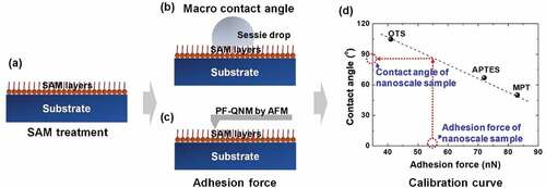
Table 1. Macro contact angle, surface energy, and adhesion force of three alkyl silane types for calibration curves.
Results and discussion
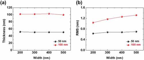
The surface morphology and wettability were investigated for the evaporated Au strip with different dimensions to observe the changes in the grain size, roughness, nano contact angle, and surface energy due to fabrication. The Au strips with a thickness (T) of 50 nm and 100 nm were deposited on SiO2 substrates using electron beam evaporation and then patterned to achieve a length (L) of 1000 nm and a variation in width (W) of 200 nm, 300 nm, 400 nm, and 500 nm by using e-beam lithography system. shows the thickness values measured using AFM. The patterned Au strips had thicknesses near the target values of 50 nm and 100 nm. However, the thickness did not vary as a function of the pattern width because the strips were patterned from identical Au thin films. The grain size evaluated from the topological AFM images revealed that the Au strips with thicknesses of 50 nm and 100 nm had grain sizes of 55 nm and 75 nm, respectively. Thus, the grain size increased with increasing Au strip thickness from 50 nm to 100 nm but did not vary significantly with the sample width. Furthermore, larger Au grains led to a higher root mean square (RMS) surface roughness, as shown in . The deposition of thin metal layers leads to a slightly increased nucleation density on the substrate and promotes the development of many small grains. In contrast, the deposition of thicker metal layers requires a longer deposition time. An increase in the substrate temperature because of the increased deposition time leads to partial degradation of the nucleation sites. Thus, further atoms are arranged in a step-by-step manner, leading to the formation of larger, highly ordered grains. In addition, the RMS values increased as the width of Au strips increased. RMS values were the average values of the scanned area of the AFM tip. Considering the tip radius of AFM tip of 125 nm, the narrow strip can result in the artificial effect on the measured RMS values coming from the large influence of the edge.
Figure 2. (a) Thickness and (b) RMS values of Au strips with the different widths measured using AFM mapping.
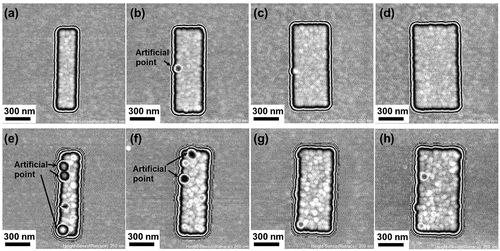
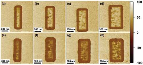
The topological AFM images that confirmed the dimensions of the Au strips are shown in . The bubble-like forms indicated by arrow were artificial points caused by edge effect. The vacuum deposition process has a significant influence on the nucleation and consequently the Au crystal growth on the silicon substrate. The substrate temperature, deposition rate (Ǻ/s), and vacuum quality during the evaporation process influence the metal strip morphology (number of Au grains and size) and surface roughness as well as the nanoscale contact angle and surface energy. Under the same deposition conditions, therefore, the morphology of the samples is governed by the thickness of the films.
Figure 3. AFM topography images of Au strips with thicknesses of (a-d) 50 nm and (e-f) 100 nm and widths of (a, e) 200 nm, (b, f) 300 nm, (c, g) 400 nm, and (d, h) 500 nm.
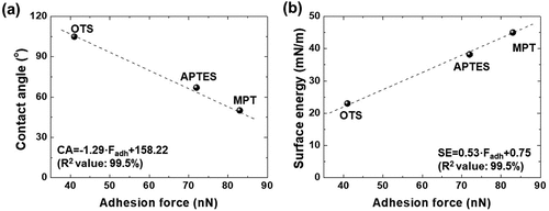
The wetting behavior, especially the nano contact angle (nCA) and surface energy (SE) of the Au strips, was determined by the nCA-AFM technique. shows the calibration plot created using the measured values listed in . The local nano contact angle or surface energy can be evaluated by translating the measured adhesion force of the Au strips from the calibration curves shown in . From the calibration curves, the general equations to calculate nCA and SE are obtained as follows:
Figure 4. Calibration plot consisting of the adhesion force from different alkyl silane self-assembled monolayers measured by AFM in PeakForce-QNM mode versus the (a) macroscopic contact angle or (b) surface energy.
where Fadh presents the measured adhesion force for the target samples.
In the PF-QNM mode of AFM, the adhesion force maps are obtained by areal scanning of the AFM tip through the entire area of the sample surfaces. shows the adhesion force maps measured for Au strips with different thicknesses and widths. A variation in the adhesion force existed due to the roughness of the samples resulting from the crystallinity of polycrystalline Au.
Figure 5. (a) AFM adhesion images of Au strips with thicknesses of (a-d) 50 nm and (e-f) 100 nm and widths of (a, e) 200 nm, (b, f) 300 nm, (c, g) 400 nm, and (d, h) 500 nm.
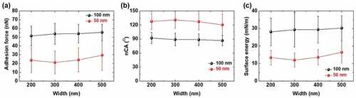
shows the average values and the standard deviation of the measured adhesion forces for Au strips. There was no significant dependence of the adhesion forces on the film width, where similar values of adhesion forces were obtained for the samples with identical thickness and varying widths. However, an increase in the thickness remarkably increased the adhesion force. The Au strips with a thickness of 100 nm showed an average adhesion force that was two times larger than that of the 50 nm strips. This is attributed to the larger grain size of 100 nm strips than that of the 50 nm strips. The adhesion forces exerted between the Au surface and AFM tips are largely influenced by the contact area, which is exclusive of the grain boundary in polycrystalline samples. In Au strips with small grains, there is a higher density of grain boundaries in the contact area with the AFM tip than that for the Au strips with large grains, which leads to smaller adhesion forces. To calculate the nCA and SE values, the measured adhesion forces are inserted into Equationequation (1)(1)
(1) Equationequation (2)
(2)
(2) . show the converted values of nCA and SE for Au strips with different thicknesses and widths from the equation obtained through the calibration curves. The measured adhesion force is inversely proportional to the nano contact angle but is directly proportional to the surface energy. Larger adhesion forces lead to smaller nCA and larger SE. There were no significant changes in the nCA and SE values of the Au strips with identical thicknesses, which was due to the similar adhesion forces. However, the thickness differences resulted in large differences in the nCA and SE values because the increased thickness remarkably increased the adhesion forces. These results highlight that the surface energy of a nanoscale metal thin film is significantly influenced by the grain size but not by the sample dimensions such as widths or thickness that lead to no change in the grain size. However, in the fabrication process using any chemical technique to make a pattern that can damage the surface of the sample, there would be a surface energy change depending on the film dimensions because of the varying degrees of chemical damage. This topic is outside the scope of this work, which aims to investigate the fundamental perspective of the surface energy of metal thin films assuming that every property is identical except the sample dimensions. However, the topic will be an interesting topic for future work.
Figure 6. (a) Measured adhesion forces and (b) translated nCA and (c) surface energy of Au strips as a function of the widths of Au strips.
Conclusion
In this study, we explored the surface energy characterization of nano-scale metal thin films using the PF-QNM mode of AFM. This method utilizes the fact that the adhesion forces are proportional to the surface energy because both physical properties are generated from surface characteristics such as functionalities or electrostatic charges. Au thin films were deposited on a SiO2 substrate to achieve thicknesses of 50 nm and 100 nm. The deposited thin films were then patterned to obtain various widths in the range from 200 to 500 nm by using e-beam lithography. Calibration curves were obtained by correlating the adhesion forces and the macro-contact angle values for the standard surfaces having different hydrophobicity values. Once the calibration curves were prepared, the surface energy or nano contact angle were evaluated by translating the measured adhesion forces into the prepared calibration curves. The surface energy in nanoscale volumes was largely governed by the grain size of the Au thin films; however, the width of the Au strip had no significant effect on the surface energy. Large grains produced larger surface energy than that of the small grains owing to the larger contact area with the AFM tip. Although the sample widths were varied, the grain size did not change since they were produced from identical Au thin films, thereby resulting in similar surface energies not dependent on the sample widths. Our study revealed that grain size control is important to design miniaturized electronic devices consisting of multi-stacked metal thin films, which are required to prevent problems such as interfacial delamination or non-homogeneous film formation resulting from surface energy mismatches.
Disclosure statement
No potential conflict of interest was reported by the author(s).
Additional information
Funding
References
- Al Maskari, N. S., M. Almobarak, A. Saeedi, and Q. Xie. 2020. Influence of pH on acidic oil–brine–carbonate adhesion using atomic force microscopy. Energy & Fuels 34 (11):13750–8. doi:10.1021/acs.energyfuels.0c02494.
- Arias, A. C., J. Devin MacKenzie, I. McCulloch, J. Rivnay, and A. Salleo. 2010. Materials and applications for large area electronics: Solution-based approaches. Chemical Reviews 110 (1):3–24. doi:10.1021/cr900150b.
- Chi, C. Y., C. C. Chang, S. Hu, T. W. Yeh, S. B. Cronin, and P. D. Dapkus. 2013. Twin-free GaAs nanosheets by selective area growth: Implications for defect-free nanostructures. Nano Letters 13 (6):2506–15. doi:10.1021/nl400561j.
- Dokukin, M. E., and I. Sokolov. 2012. Quantitative mapping of the elastic modulus of soft materials with HarmoniX and PeakForce QNM AFM modes. Langmuir 28 (46):16060–71. doi:10.1021/la302706b.
- Fan, F. R., W. Tang, and Z. L. Wang. 2016. Flexible nanogenerators for energy harvesting and self-powered electronics. Advanced Materials (Deerfield Beach, Fla) 28 (22):4283–305. doi:10.1002/adma.201504299.
- Gazze, S. A., S. J. Thomas, J. Garcia-Parra, D. W. James, P. Rees, V. Marsh-Durban, R. Corteling, D. Gonzalez, R. S. Conlan, and L. W. Francis. 2021. High content, quantitative AFM analysis of the scalable biomechanical properties of extracellular vesicles. Nanoscale 13 (12):6129–41. doi:10.1039/d0nr09235e.
- Hamieh, T. 2022. New methodology to study the dispersive component of the surface energy and acid–base properties of silica particles by inverse gas chromatography at infinite dilution. Journal of Chromatographic Science 60 (2):126–42. doi:10.1093/chromsci/bmab066.
- Holec, D., P. Dumitraschkewitz, D. Vollath, and F. D. Fischer. 2020. Surface energy of Au nanoparticles depending on their size and shape. Nanomaterials (Basel) 10 (3). doi: 10.3390/nano10030484.
- Hong, S., H. Lee, J. Lee, J. Kwon, S. Han, Y. D. Suh, H. Cho, J. Shin, J. Yeo, and S. H. Ko. 2015. Highly stretchable and transparent metal nanowire heater for wearable electronics applications. Advanced Materials 27 (32):4744–51. doi:10.1002/adma.201500917.
- Hwang, B., and T. Gwang Yun. 2019. Stretchable and patchable composite electrode with trimethylolpropane formal acrylate-based polymer. Composites Part B: Engineering 163:185–92. doi:10.1016/j.compositesb.2018.11.009.
- Khatri, N. R., X. Ji, H. K. Minsky, and Y. Jiang. 2021. Understanding nanoscale topology–adhesion relationships via support vector regression. Advanced Materials Interfaces 8 (14). doi: 10.1002/admi.202100175.
- Kiesvaara, J., and J. Yliruusi. 1993. The use of the Washburn method in determining the contact angles of lactose powder. International Journal of Pharmaceutics 92 (1):81–88. doi:10.1016/0378-5173(93)90266-I.
- Kim, H., G. Lee, S. Becker, J.-S. Kim, H. Kim, and B. Hwang. 2018. Novel patterning of flexible and transparent Ag nanowire electrodes using oxygen plasma treatment. Journal of Materials Chemistry C 6 (35):9394–98. doi:10.1039/C8TC02377H.
- Kozbial, A., Z. Li, C. Conaway, R. McGinley, S. Dhingra, V. Vahdat, F. Zhou, B. D’Urso, H. Liu, and L. Li. 2014. Study on the surface energy of graphene by contact angle measurements. Langmuir 30 (28):8598–606. doi:10.1021/la5018328.
- Li, L., C. Liu, Y. Su, J. Bai, J. Wu, Y. Han, Y. Hou, S. Qi, Y. Zhao, H. Ding, et al. 2018. Heterogeneous integration of microscale GaN light-emitting diodes and their electrical, optical, and thermal characteristics on flexible substrates. Advanced Materials Technologies 3 (1):1700239. doi:10.1002/admt.201700239.
- Moghadam, R., M. H. E. Zarei, H. Rezagholipour Dizaji, P. Kameli, and M. Jannesari. 2018. Modification of hydrophobicity properties of diamond like carbon films using glancing angle deposition method. Materials Letters 220:301–04. doi:10.1016/j.matlet.2018.03.060.
- Neirinck, B., J. Van Deursen, O. Van der Biest, and J. Vleugels. 2010. Wettability assessment of submicrometer alumina powder using a modified washburn method. Journal of the American Ceramic Society 93 (9):2515–18. doi:10.1111/j.1551-2916.2010.03854.x.
- Niu, C., W. Xia, and Y. Peng. 2018. Analysis of coal wettability by inverse gas chromatography and its guidance for coal flotation. Fuel 228:290–96. doi:10.1016/j.fuel.2018.04.146.
- Otyepkova, E., P. Lazar, J. Luxa, K. Berka, K. Cepe, Z. Sofer, M. Pumera, and M. Otyepka. 2017. Surface properties of MoS2 probed by inverse gas chromatography and their impact on electrocatalytic properties. Nanoscale 9 (48):19236–44. doi:10.1039/c7nr07342a.
- Park, W., S. Müller, R.-P. Baumann, S. Becker, and B. Hwang. 2020. Surface energy characterization of nanoscale metal using quantitative nanomechanical characterization of atomic force microscopy. Applied Surface Science 507. doi:10.1016/j.apsusc.2019.145041.
- Polaki, S. R., P. A. Gopinath Sahoo, N. G. Krishna, S. Kamruddin, and M. Dhara. 2021. Engineering the edge-terminations and defect-density to enhance the electrochemical capacitance performance of vertical graphene nanosheets. Applied Surface Science 545: 149045. doi:10.1016/j.apsusc.2021.149045.
- Qaiser, N., F. Al-Modaf, S. Munsif Khan, S. Faizan Shaikh, N. El-Atab, and M. Mustafa Hussain. 2021. A robust wearable point-of-care CNT-based strain sensor for wirelessly monitoring throat-related illnesses. Advanced Functional Materials 31 (29):2103375. doi:10.1002/adfm.202103375.
- Sui, Y., Y. Cui, X. Meng, and Q. Zhou. 2021. Research progress on the correlation between properties of nanoparticles and their dispersion states in polymer matrix. Journal of Applied Polymer Science 139 (19):52096. doi:10.1002/app.52096.
- Xiong, J., J. Di, J. Xia, W. Zhu, and H. Li. 2018. Surface defect engineering in 2D nanomaterials for photocatalysis. Advanced Functional Materials 28 (39). doi: 10.1002/adfm.201801983.
- Xu, H., H. Shang, C. Wang, and Y. Du. 2020. Low‐dimensional metallic nanomaterials for advanced electrocatalysis. Advanced Functional Materials 30 (50). doi: 10.1002/adfm.202006317.
- Zaman, N., R. Ahmed Malik, H. Alrobei, J. Kim, M. Latif, A. Hussain, A. Maqbool, R. Abdul Karim, M. Saleem, and M. Asif Rafiq. 2020. Structural and electrochemical analysis of decarburized graphene electrodes for supercapacitor applications. Crystals 10 (11):1043.
- Zhang, F., E. Mohammadi, X. Luo, J. Strzalka, J. Mei, and Y. Diao. 2018. Critical role of surface energy in guiding crystallization of solution-coated conjugated polymer thin films. Langmuir 34 (3):1109–22. doi:10.1021/acs.langmuir.7b02807.