Abstract
A MEMS deformable mirror (DM) packaging process development effort is described. This development provides a path towards direct integration of future large actuator count optical MEMS arrays (> 4000) with underlying driver electronics. Characteristic features of the packaging process include creating electrical interconnection paths through the silicon wafer for each actuator, depositing gold bump bonds on the backside of the wafer, and fusing that array of bump bonds to an interposer substrate. This process differs from existing processes for MEMS arrays, which generally employ lithographically patterned wire-routing and peripheral wire bonding from the front surface of the MEMS array. In this article a feasibility experiment is described and successful results and process parameters are presented.
1. INTRODUCTION
MEMS Deformable mirrors DMs have become an indispensable and enabling component in adaptive optics systems that compensate aberrations and improve resolution in microscopes and telescopes (Potsaid, Bellouard, and Wen, Citation2005; Leray and Mertz, Citation2006; Gavel et al., Citation2008). They have been produced in arrays of up to 4096 actuators (64 × 64) on square pitch of 400 µm, corresponding to a total aperture size of about 25 mm (Cornelissen et al., Citation2009). In future large telescope applications, especially those for high-contrast exoplanet imaging, DMs with up to 10,000 actuators are needed (Dekany et al., Citation2004). A principal challenge for DMs with larger actuator arrays involves interconnection to driver electronics, where each actuator has a dedicated high voltage driver channel. This requires the development of innovative packaging solutions capable of overcoming the limitations of conventional approaches, which have reached the limit of their scalability at current actuator counts.
The approach used for packaging commercial MEMS DMs to date has involved dedicating one or more fabrication process layers to wire routing on the surface of the device substrate, and to use these routing lines to connect electrostatic actuator electrodes to a ring of lithographically-defined, gold-coated bond pads at the periphery of the MEMS DM die. After attaching the MEMS die to the cavity of a custom-manufactured ceramic chip carrier using a low-modulus adhesive, each die bond pad is connected to a corresponding package bond pad using an automated wire-bonding tool. This approach is not scalable; fan out from a two-dimensional actuator array to a one-dimensional bond-pad array means that the die area required for the device grows in proportion to the square of its number of actuators.
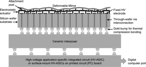
As actuator count increases, this nonlinear increase in die area reduces the number of yielding die in a conventional MEMS foundry process to an untenable level. This is a result of having fewer die on a wafer, as well as an increase in defect probability, which is proportional to die area. The MEMS layer dedicated to wire routing lines is particularly susceptible to yield failure due to processing defects and contamination, since wire routing lines are sized and spaced at the resolution limits of the fabrication process. Also, the number of interconnects provided by state-of-the-art ceramic chip carrier is limited to about 5000 elements, which means this packaging solution has reached its scalability limit, although MEMS DMs have not. The goal of this effort was to demonstrate the feasibility of using through-wafer electrical interconnects to address MEMS DMs instead wire bonds, by combining a commercially available through-wafer-via manufacturing process with the standard MEMS DM fabrication processes. The concept is illustrated in Figure for a MEMS DM bonded to an interposer and then to an electronics drive array.
Figure 1 Cross sectional schematic of the overall device concept. A MEMS DM is anchored by attachment posts to a large array of electrostatic actuators. Actuators consist of compliant electrodes suspended over fixed electrodes. When voltage is applied to a fixed electrode, the corresponding compliant electrode deflects, exerting a force on the mirror through the attachment post. Electrical connection to the fixed electrode array is made using through-wafer vias that transect the silicon wafer. Each via is comprised of an electrically conductive core and an insulating sleeve. On the bottom side of the wafer, each via terminates on a conductive pad. Gold hemispherical bumps are deposited on the pads through a high-yield ultrasonic/thermal deposition technique. These bonds are fused to corresponding bumps on a custom-manufactured ceramic interposer through a precise “flip chip” process in which mating gold bumps are aligned, heated, and compressed. The interposer, in turn, is flip-chip bonded to a high voltage electronic drive circuit that can be directly controlled by a computer.
Through wafer via (TWV) technology allows integration of device interconnects by way of electrically conductive pathways manufactured into the wafer substrate before DM processing. At least one foundry aims at making the process an industry standard, and its application for optical MEMS devices has been previously studied by researchers at Sandia National Laboratories (Frederick and McCormick, Citation2008). Several approaches to high-yield array interconnection using TWVs have been developed. The work presented here evaluated the use of gold thermo-compression bonding, which is a standard in the IC packaging industry, in conjunction with TWVs to establish a path towards high actuator count MEMS DM packaging solutions.
The flip chip bonding method was originally developed for wafer scale semiconductor hybrid packaging, and employed lead-tin solder bump interconnection in a process introduced by IBM in the early 1960s (Lee, Lee, and Jen, Citation2000). The gold stud flip-chip bonding process subsequently developed for MEMS is often used as a low-volume, die level packaging approach (Lau, Citation1995; Aschenbrenner, Miessner, and Reichl, Citation1997; Chuang, Citation2007). It connects the MEMS die to a circuit board, electronics chip, or interposer and makes electrical contact to gold bumps using adhesives, thermosonic assembly, or thermo-compression bonding. The adhesive method is often preferred when bonding temperature or bonding force is required. An additional advantage is that the adhesive can compensate for small variations in gold bump height across the array. It can also relax the coplanarity requirements for metal to metal bonding. A limitation of the adhesive method is that it complicates hydrofluoric release of the MEMS device following the bonding. Researchers at Sandia National Laboratories reported partial success with an epoxy that survived an HF-HCl release process but acknowledged that more testing was required for this process (Jagt, Citation1998). In flip chip thermo-compression bonding, complementary arrays of metal bumps are deposited on both chips to be bonded. The bump arrays are aligned and contacted, and then force and heat are applied to soften metal bond material, resulting in reflow and fusing. Temperature, bonding force, and time typically range 200–500° C, 50–600 g per bump, and 5–10 s. The effects of these three parameters on the bonding mechanism have been reported for various special bonding cases (Frederick and McCormick, Citation2008; Jellison, Citation1975; Ang, Citation2006). While bonding can occur at room temperature, larger force is generally needed in that case. Thermosonic bonding is analogous to thermo-compression bonding with the exception that the gold bumped die is subjected to another form of energy in addition to being placed under heat and pressure. The addition of the ultrasonic energy lowers the requirements for heat (Condra, Svitak, and Pense, Citation1975; Joshi, Citation1971). Gold-gold thermo-compression bonding was the primary flip-chip assembly process explored in this work. Packaging experiments involved bonding the MEMS DM actuator array devices to interposer die that were fabricated separately and contained bump bond pads produced using a single gold deposition and patterning step. The interposer is not necessarily required: MEMS array chips could in principle be bonded directly to electronic driver chips using this process. However, the circuits required for driving MEMS DM electrostatic actuators feature high voltages (> 100 V) and high precision (> 8 bits), and it is unclear that the packing factor achieved in the DM chip (400 µm pitch) could be achieved in the electronics driver array. With an intermediate interposer chip, the actuator array connections on the backside of the MEMS chip could be fanned out to an electronics driver array having larger pitch.
2. FABRICATION AND ELECTROMECHANICAL CHARACTERIZATION
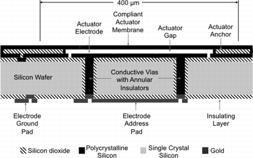
For this work, a lithographic mask set was modified to accommodate the through-wafer interconnects. The mask set was provided by Boston Micromachines Corporation (BMC), and was adapted from a commercially available BMC deformable mirror device. The arrays were comprised of 144 electrostatic actuators in a 12 × 12 square grid. A cross-sectional schematic of one actuator in the array is detailed in Figure . The devices were made using two separate MEMS foundries. Through-wafer interconnect fabrication was performed at IceMOS Technology, a commercial foundry specializing in supplying pre-processed silicon substrates for MEMS fabrication. Wafers measuring 300 µm thick and 150 mm were first thermally oxidized to form a silicon dioxide film that was lithographically patterned and etched as a mask layer. Holes measuring ∼30 µm in diameter were then etched through the wafer using a deep reactive ion etching process. An oxide layer was deposited on the interior of the etched holes to electrically isolate them from the silicon substrate. The holes were then filled using doped polycrystalline silicon in a vapor deposition process. Subsequently, the wafers were polished on both sides to remove the surface oxide layer and to planarize the surface, thereby completing the via production process. Actuator structures and metal pad connections were fabricated using MEMSCAP, a commercial foundry specializing in silicon surface micromachining. A thin film of polycrystalline silicon (0.5 µm) was deposited on the wafers, lithographically patterned, and etched using reactive ion etching to form the actuator electrodes. Next, a thin film of sacrificial oxide (5 µm) was deposited, patterned, and etched to provide the electrostatic actuator gaps and the actuator anchors. A second thin film of polycrystalline silicon (2 µm) was deposited, patterned, and etched to form the compliant actuator membrane structures. A silicon nitride layer was deposited on the backside to provide electrical insulation between the TWVs and the substrate. Finally, a thin film of gold (50 nm) was deposited, patterned, and etched on the backside of the wafer to provide electrical contact pads.
Figure 2 Cross-sectional schematic of one actuator in the actuator array fabricated with through-wafer interconnections for this project.
The wafers were then diced into individual die after which the sacrificial oxide was removed using hydrofluoric acid (HF) resulting in the released MEMS actuator arrays with integrated through-wafer interconnects.
While the present work involved only fabrication of actuator arrays, the MEMS process used to make deformable mirrors involves only three more surface micromachining steps: deposition, patterning, and etching of a second sacrificial oxide layer; deposition, patterning, and etching of a polycrystalline silicon mirror layer; and deposition of a thin reflective metal layer on the mirror. These MEMS DM process steps and fabrication have been described in detail elsewhere (Perreault et al., Citation2002; Mali et al., Citation1997; Mali, Bifano, and Koester, Citation1999; Cornelissen et al., Citation2009; Bifano et al., Citation1999, Citation1997).
The gold bond pad arrays were fabricated on the backside of the actuator device die (the TWV interconnects) and on the surface of an interposer die using a process developed and carried out at BU. Gold contact pads measuring 200 µm in diameter were deposited in an array corresponding to the TWV interconnect locations a 400 µm square pitch. To test the electrical connectivity of the bump bonded electrostatic actuator array, the interposer bond pads were connected to wire bond pads on the periphery of the die using surface routed wires, providing that the die could be packaged using conventional means (wire bonding to a ceramic chip carrier pin grid array) and voltage applied to the actuators. To accommodate for planarity errors between the surfaces of the two die and to improve the adhesion of adjoined bond pads, an array of gold studs or bumps are placed on the interposer die prior to bonding. This is performed using an Esec 3018 automated wire bonding system.
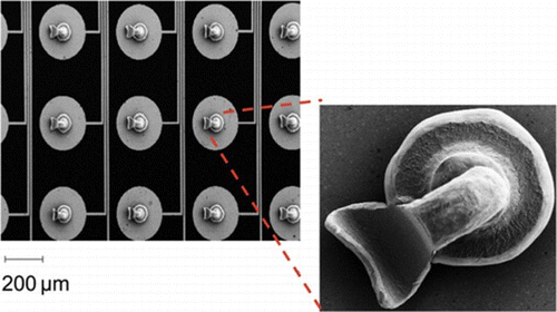
Standard ball-wedge wire bonding capillaries are used and are capable of producing bumps consistently having predictable, repeatable geometry. The process produces roughly hemispherical bumps with short tails. This unusual geometry of the gold bump is not important in the flip-chip bonding process presented here as long as the bumps are consistent in size and smaller than the bond pads. Specialized ball bumping capillaries and wire do exist that are capable of producing gold studs with cylindrical shape. All bumps are flattened in the subsequent thermal compression process. The bumping process developed in this work used a 25 µm diameter gold wire, and produced bump sizes ranging from 70 to 80 µm in diameter and 50 to 80 µm in height. Scanning electron microscope images of a portion of the bump bond array on the interposer chip are shown in Figure . Each bump bond is deposited on a gold pad, and each pad is connected by a surface-routed wire trace to the periphery of the interposer board, where it can be probed or energized using off-board electronics. A complementary array of bond pads without the wire traces was deposited on the back of the MEMS chip.
Figure 3 Scanning electron microscope images of images of a portion of the bump bond array (4 × 3 shown, plus close up of one bond) on the interposer chip. Each bump bond is deposited on a gold pad, and each pad is connected by a surface-routed wire trace to the periphery of the interposer board, where it can be probed or energized using off-board electronics. A complementary array of bond pads (without the corresponding wire traces) was deposited on the backside of the MEMS chip. (Figure is provided in color online.).
From preliminary bonding experiments using silicon chips, a baseline process was identified for the TWV and interposer die. It consisted of initial heating to 150°C for alignment, followed by additional heating to the bonding temperature (250°C–300°C) over a 10–30 second period, substrate-chip contact using a bonding force between 2 to 10 kg for 10–30 seconds, and then cooling. Using these baseline parameters, several test bonds were first performed on TWV and interposer die to evaluate the effectiveness of the test sample process on these different devices using new custom tooling, which contained a cavity located over the array of released electrostatic actuators, applying bonding pressure only to the perimeter of the chip. One of the primary challenges of this process development was preventing damage to the freed MEMS DM actuators in the bonding process. These results were then used to develop a design of experiment (DOE) for identifying an ideal bonding recipe.
Several variables were used to characterize the quality of the flip-chip bonding process, including the electromechanical yield of the bonded actuator array, as well as residual stress in the bonded TWV die. Management of this stress is important for maintaining the surface figure of flip-chip bonded DMs, which require surface flatness tolerances of a few hundred nanometers. Stress in the bonded die was evaluated through changes in substrate curvature, as well as changes in the shape of the unpowered electrostatic actuator diaphragm. Change in die curvature provides a quantitative measure of the change in average residual stress in the die, where a change in actuator sag provides information about the local distribution of that stress.
An 8-run, 3-factor (temperature, pressure, and time), 2-level, full factorial DOE was performed using a commercial die-bonding tool (Smart Equipment Technology FC 150). The three factors varied were bonding time, bonding temperature, and bonding force. The metric used to evaluate bond quality was the change in TWV die radius of curvature, which is a quantitative measure of residual stress in the bonded die. The purpose of the DOE was to identify the influence of these parameters on bond quality from inferred values for die stress. Curvature change was measured using a surface mapping interferometric microscope, which can measure surface topography with nanometer-scale precision. The maximum radius of curvature profile measured across the 12 × 12 actuator area was used as a quantitative measure of bonding performance (i.e., response factor) in the DOE. The DOE response factor was defined to be the change in curvature before and after bonding. The input factors and levels for the DOE, selected based on outcomes of preliminary bonding experiments, are summarized in Table .
Table 1. Parameter values tested in full factorial experiments (DOE) to assess impact of thermo-compression bonding force, temperature, and holding time on bond quality
The results of the DOE, suggest that the optimum gold thermo-compression bonding recipe for the TWV and interposer die are 5500 g applied bonding mass for 10 seconds at 325°C. They further suggest that the primary bonding parameter affecting the response factor was bonding force.
The electromechanical performance of the electrostatic actuator array was also evaluated for each sample bonded in the DOE. After bonding, chip stacks were packaged using a ceramic pin grid array. A commercial high voltage driver was used to individually control each of the actuators on the TWV die one at a time.
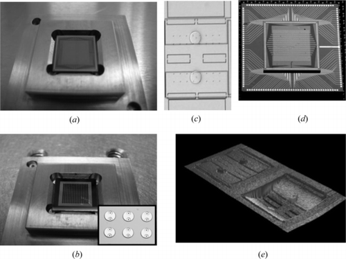
Figure illustrates some features of the device before and after bonding and testing. Included are photographs of the MEMS chip and the interposer chip, before bump deposition (Figures 4a and 4b), and after bump deposition and bonding (Figure d). Also shown is a high-resolution microscope image of one actuator (Figure c) and an interferometric surface map of an actuator deflected by 1.2 µm using the TWV interconnection (Figure e) to apply a 250 V potential across its electrodes.
Figure 4 Images of a 140 actuator MEMS DM actuator array chip with integrated through-wafer vias (TWVs); (a): 10 mm die with 140 electrostatic actuators produced on TWV substrate. (b): Bottom of the device, showing gold pads with two TWV interconnects per actuator; (c): Microscope image of a single actuator's surface. (d): Photo of flip chip bonded actuator array on a 10 mm square TWV substrate and bonded to an interposer test PC board through vertical bump bond interconnections; (e): Measured surface deformation of an actuator subjected to 200 V through TWV connection. Peak deflection of 1.2 µm was obtained.
Actuator failures were observed and traced to failed flip-chip connections, damaged wires on the surface of the interposer die, or manufacturing problems with the fabrication of the actuator array. From these tests it was determined that actuator yield was highly correlated with post-bonding change in die curvature. Samples with more than 5 m radius of curvature change yielded poorly (all less than 50% yield—some with noticeable actuator damage). The sample with the highest actuator yield (92%) experienced the least amount of curvature change (2 m). This sample was bonded using the low force, low temperature, high time split of the DOE.
3. CONCLUSIONS
A successful thermo-compression flip-chip assembly and packaging process for bonding DM electrostatic actuator arrays with TWV interconnects to interposer die has been developed. The methodology of using an interposer board for reducing connection density was also demonstrated to be useful. A flip-chip process capable of producing low stress bonded die was developed and is expected to be successful for fully functional DMs with greater actuator counts in future work.
REFERENCES
- Ang , X. F. 2006 . Temperature and pressure dependence in thermocompression gold stud bonding . Thin Solid Films 504 ( 1–2 ): 379 – 383 .
- Aschenbrenner , R. , R. Miessner , and H. Reichl . 1997 . Adhesive flip chip bonding on flexible substrates . Journal of Electronics Manufacturing 7 ( 4 ): 245 – 252 .
- Bifano , T. G. , R. K. Mali , J. K. Dorton , J. Perreault , N. Vandelli , M. N. Horenstein , and D. A. Castanon . 1997 . Continuous-membrane surface-micromachined silicon deformable mirror . Optical Engineering 36 ( 5 ): 1354 – 1360 .
- Bifano , T. G. , J. Perreault , R. K. Mali , and M. N. Horenstein . 1999. Microelectromechanical deformable mirrors. Journal of Selected Topics in Quantum Electronics 5(1):83–89.
- Chuang , C. L. 2007 . Increasing bondability and bonding strength of gold stud bumps onto copper pads with a deposited titanium barrier layer . Microelectronic Engineering 84 ( 4 ): 551 – 559 .
- Condra , L. W. , J. J. Svitak , and A. W. Pense . 1975 . The high temperature deformation properties of gold and thermocompression bonding . IEEE Transactions on Parts, Hybrids, and Packaging 4 : 290 – 296 .
- Cornelissen , S. A. , P. A. Bierden , T. G. Bifano , and C. V. Lam . 2009 . 4096-element continuous face-sheet MEMS deformable mirror for high-contrast imaging . Journal of Micro/Nanolithography, MEMS and MOEMS 8 ( 3 ): 031308-8 .
- Dekany , R. G. , M. C. Britton , D. T. Gavel , B. L. Ellerbroek , G. Herriot , C. E. Max , and J-P. Veran . 2004 . Adaptive optics requirements definition for TMT . SPIE Advancements in Adaptive Optics 5490 : 879 – 890 .
- Frederick , S. and F. McCormick . 2008 . Integrated optical MEMS using through-wafer vias and bump-bonding. Sandia National Laboratories Report SAND2008–0256.
- Gavel , D. , S. Severson , B. Bauman , D. Dillon , M. Reinig , C. Lockwood , D. Palmer , K. Morzinski , M. Ammons , E. Gates , and B. Grigsby . 2008 . Villages: An on-sky visible wavelength astronomy AO experiment using a MEMS deformable mirror . MEMS Adaptive Optics II SPIE 6888 : 688804 – 688807 .
- Jagt , J. C. 1998 . Reliability of electrically conductive adhesive joints for surface mount applications: A summary of the state of the art . IEEE Transactions on Components Packaging and Manufacturing Technology, Part A 21 ( 2 ): 215 – 225 .
- Jellison , J. 1975 . Effect of surface contamination on the thermocompression bondability of gold . IEEE Transactions on Parts, Hybrids, and Packaging 11 ( 3 ): 206 – 211 .
- Joshi , K. C. 1971 . The formation of ultrasonic bonding between metal . Welding 50 : 840 – 848 .
- Lau , J. H. 1995 . Flip chip technologies . New York : McGraw-Hill .
- Lee , C.-C. , T.-Y. Lee , and Y.-J. Jen . 2000 . Ion-assisted deposition of silver thin films . Thin Solid Films 359 ( 1 ): 95 – 97 .
- Leray , A. and J. Mertz . 2006 . Rejection of two-photon fluorescence background in thick tissue bydifferential aberration imaging . Optics Express 14 ( 22 ): 10565 – 10573 .
- Mali , R. K. , T. G. Bifano , N. Vandelli , and M. N. Horenstein . 1997 . Development of microelectromechanical deformable mirrors for phase modulation of light . Optical Engineering 36 ( 2 ): 542 – 548 .
- Mali , R. K. , T. Bifano , and D. Koester . 1999 . A design-based approach to planarization in multilayer surface micromachining . Journal of Micromechanics and Microengineering 9 ( 4 ): 294 – 299 .
- Perreault , J. A. , T. G. Bifano , B. M. Levine , and M. N. Horenstein . 2002 . Adaptive optic correction using microelectromechanical deformable mirrors . Optical Engineering 41 ( 3 ): 561 – 566 .
- Potsaid , B. , Y. Bellouard , and J. Wen . 2005 . Adaptive scanning optical microscope (ASOM): A multidisciplinary optical microscope design for large field of view and high resolution imaging . Optics Express 13 ( 17 ): 6504 – 6518 .