Abstract
The heat dissipation through interchip structures was investigated by introducing 4-partition and 16-partition ceramic interchip structures for a 16-chip light-emitting diode (LED) package. Using the finite volume method simulation with ICEPAK V13.0, the temperature distribution inside the LED package and the junction temperature were estimated, from which the effect of the interchip structures on the heat dissipation characteristics of the LED package was investigated. The results showed that the ceramic interchip structures provided a more effective upward heat dissipation path for the LED package and contributed to a 23°C decrease in the junction temperature for the 4-partition interchip structure and a 51°C decrease for the 16-partition interchip structure at the 16 W operation.
1. Introduction
Heat dissipation is one of the core problems that must be solved to achieve reliable light-emitting diode (LED) performance Citation1. As an increase in the chip junction temperature degrades the conversion efficiency Citation2. The higher the current injection level, the more the heat generated from the LED, which causes a severe problem if not efficiently dissipated. Therefore, an LED manufacturer must provide the most efficient thermal dissipation path possible and balance it with other design factors such as the physical dimensions and optical performance and cost Citation3. Currently, high-power multichip LED packages that have dozens of single LED chips are attracting much interest due to their characteristics as surface light sources. In this case, heat dissipation becomes more important as the power consumption increases and the LED chips come closer to each other Citation4.
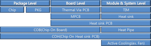
shows the classification of the heat dissipation technologies for an LED package into the package level, board level, and module and system level. For the package level, the typical technologies include eutectic bonding to decrease the interface thermal resistance between the chip and the electrode Citation5, and the via hole method with high thermal conductivity Citation6; for the board level, chip on board packaging Citation7; and for the module and system level, the heat pipe and Peltier element Citation8 methods and forced convection using a fan Citation9. All these methods are related to the downward heat dissipation of the package, in which effective heat dissipation is conducted through the large surface area of the metal-core printed circuit board (MPCB) or heat sink. Although upward heat dissipation is not as effective as downward dissipation, it is also important for high-power multichip LED packages.
Figure 1. Classification of the heat dissipation technologies for the LED package.
The purpose of this study is to investigate the upward thermal dissipation of an LED package through a silicon mold and a ceramic package. We have reported on the experimental results for 4-partition interchip structure, in which only 2.5 W input power was applied to avoid the failure of the package due to the heat Citation10. In this study, two kinds of ceramic interchip structures, 4-partition and 16-partition, are compared to ensure the utility of the interchip structure under 16 W input power in maximum via a simulation work.
2. Experiments
2.1. Modeling of the LED package
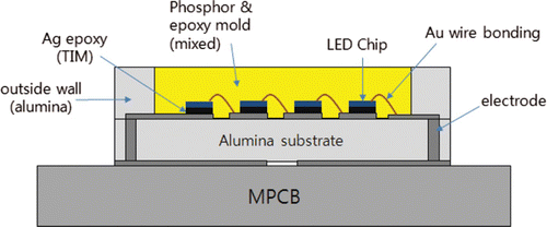
shows a schematic of the 16-chip LED package that was used in this study. The package has a thermal via structure that serves as the electrical connection between the chip and the circuit electrode in a vertical LED chip. The positive polarity electrodes of each LED chip are electrically connected through wire bonding. In this study, 16 LED chips were placed within a submount package, and the package was filled with yellow phosphor mixed with a silicon mold as an encapsulant, as shown in . Blue vertical InGaN LED chips were used, which were bonded with the ceramic submount using Ag epoxy as the thermal interface material (TIM). Then the submount was bonded with the MPCB using a Pb–Sn solder. The bottom dimensions of each LED chip were about 1 mm×1 mm, and of the submount, about 12 mm×12 mm. Each LED chip was 0.17 mm thick, and the outside wall that was used to hold the yellow phosphor in the package was 0.7 mm high. The MPCB was mainly made of aluminum.
Figure 2. Dimensions and structure of the LED package in this study.
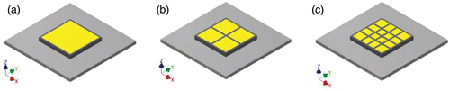
shows the designs of the three kinds of packages used in this study. shows the design of the 16-chip package with a conventional structure, in which the outside wall was made of ceramic as was the substrate. shows the design of the 4-partition interchip structures in which horizontal and vertical interchip structures were introduced into the space between the LED chips. The interchip structure was made of ceramic, as was the substrate, and the distance between the interchip structure and the chip was about 0.63 mm, which is narrower than the distance between the chip and the outside wall of 1.3 mm. As shown in the figure, there were 16 contact points (marked by dotted circles) for this structure. shows the design of the 16-partition interchip structures in which there were 48 contact points (marked by dotted circles). shows the LED package models used in the finite volume method (FVM) simulations.
Figure 3. Design of the packages used in this study. (a) Conventional structure, (b) proposed structure with the 4-partition interchip structures, and (c) proposed structure with the 16-partition interchip structures.
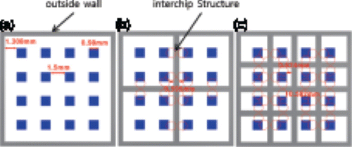
Figure 4. LED package models used in the FVM simulations. (a) Conventional structure, (b) with the 4-partition interchip structures, and (c) with the 16-partition interchip structures.
2.2. Simulation modeling
Mesh-size-independent analyses were performed before the simulation. Since free convection occurs at the boundary, the surrounding temperature was fixed at 25°C. In natural convection, the Rayleigh number (Ra) is an important factor in determining the flow properties, in which a turbulent flow is assumed when Ra>109 and a laminar flow occurs when Ra<109. The Ra was calculated as follows:
Ra is expressed as
To analyze the heat transfer via heat convection, the law of mass–momentum–energy conservation was considered in the form of the Navier–Stokes equation:
Heat is generated from the p–n junction area of the LED chip and dissipated through the surfaces of the package. Eighty percent of the electrical power consumption of the LED package is assumed to be transferred in the form of heat flux energy from the junction to the surfaces of the package, including the MPCB and the epoxy mold. Therefore, the heat generation for each chip was determined by dividing 80% of the electrical power consumption by the number of chips. The hexahedron mesh was maximally created using the Mesher-HD type included in the ICEPAK's mesh types. shows the material properties of each component, which were used as input variables for the simulation.
Table 1. Material properties of the components of the LED package.
3. Results and discussion
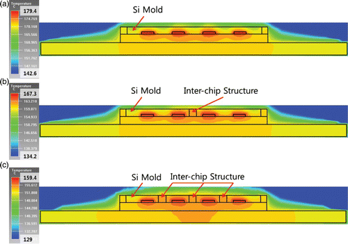
shows the cross-section of the simulated results of the temperature distribution inside the LED package when the input power was 4.5 W. In the figure, the maximum temperature was found at the p–n junction of the LED chip, which is called the junction temperature (T J). The junction temperature was estimated to be about 179°C for the conventional structure, which decreased to about 167°C and 159°C for the proposed structures with the 4-partition and 16-partition interchip structures, respectively. This decrease in the junction temperature was due to the heat conduction through the new contact points, as explained in .
Figure 5. Cross-section of the simulated results of the temperature distribution inside the LED package when the input power was 4.5 W. (a) Conventional structure, (b) with the 4-partition interchip structures, and (c) with the 16-partition interchip structures.
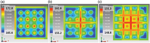
To investigate the heat flow between the chips, a simulation was conducted for the top surface temperature of the package shown in . The figure shows that the maximum top surface temperature decreased from about 173°C for the conventional structure to 163°C and 155°C for the 4-partition and 16-partition interchip structures, respectively. As mentioned in , there were 16 and 48 contact points (marked by dotted circles) for the 4-partition and 16-partition interchip structures, respectively, which caused a difference in the surface areas of the interchip structures. As the heat dissipation through the interchip structures was conducted via the convection on their top surfaces, the top surface temperature was of course lowest for the 16-partition interchip structures, as shown in .
Figure 6. Top view of the simulated results of the surface temperature distribution of the LED package when the input power was 4.5 W. (a) Conventional structure, (b) with the 4-partition interchip structures, and (c) with the 16-partition interchip structures.
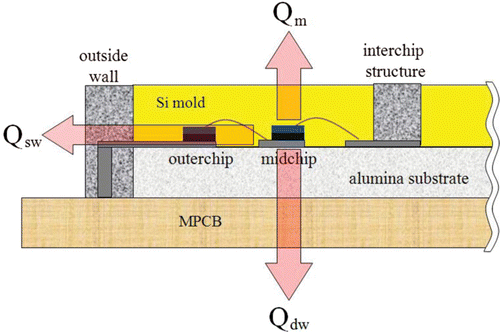
In , the top surface temperature of the ceramic interchip structure was higher than that of the silicon mold, which means that the heat dissipation through the top surface of the partition interchip structure was more effective. also shows that the top surface temperatures of the midchips were higher than those of the outerchips. To investigate this difference, the junction temperatures of the chips of the LED package were compared via FVM simulation, as shown in . It should be noted that the temperature in is the junction temperature. In the figure, T c is the average surface temperature of the four midchips, and T s, of the 12 outerchips; and Δ T is T c−T s in the same package. shows that T c was higher than T s in all the cases, which can be explained as follows. shows the heat dissipation model proposed in this study, in which the total heat radiated from the p−n junction of the LED was dissipated in three directions; toward the mold and the outside wall, and downward. The heat dissipation rates in these three directions were expressed as Q m, Q sw, and Q dw, respectively. The following well-known equation can be considered Citation10:
Figure 7. Comparison of the junction temperatures of the chips by FVM simulation. (a) Conventional structure, (b) with the 4-partition interchip structures, and (c) with the 16-partition interchip structures.
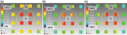
Figure 8. Heat dissipation model proposed in this study.
shows a plot of the Δ T that was determined in , with the input power varied up to 16 W. It could be seen that Δ T was smaller for the proposed structure than for the conventional one, and shows the smallest Δ T due to the 16-partition interchip structures. This is explained in the following manner using the heat dissipation model in . The ceramic interchip structures were positioned between the LED chips, so a part of the silicon mold was replaced with the ceramic interchip structures. Therefore, the heat dissipation rates in the direction of the top surface of the silicon mold, Q m, is expressed as
Figure 9. Plot of the Δ T determined in according to the input power. (a) Conventional structure, (b) with the 4-partition interchip structures, and (c) with the 16-partition interchip structures.
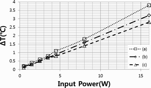
Figure 10. Thermal equivalent circuit of the heat dissipation through the top surface of the LED package.
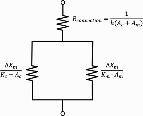
In this model, the total thermal resistance can be expressed as
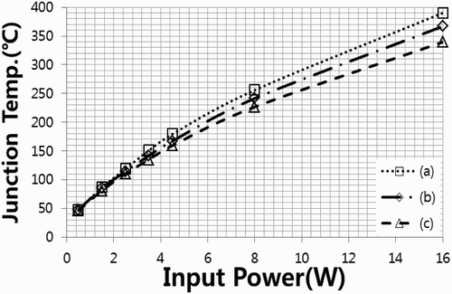
In conclusion, for the proposed structure in this study, the ceramic interchip structures replaced some parts of the silicon mold between the LED chips, which provided a more effective upward heat dissipation path for the midchips due to the higher thermal conductivity of the ceramic and contributed to the decrease in the junction temperature of the midchips. shows the change in the junction temperature with the input power that was estimated via FVM simulation, which shows that the differences in the junction temperatures in (a)–(c) increase with the input power. Ultimately, the junction temperature could be decreased by 23°C and 51°C due to the 4-partition and 16-partition interchip structures under 16 W operation, respectively.
Figure 11. Change in the junction temperature with the input power. (a) Conventional structure, (b) with the 4-partition interchip structures, and (c) with the 16-partition interchip structures.
4. Conclusion
For a high-power multichip LED package, upward heat dissipation through the top surface of the silicon mold should be considered. As the thermal conductivity of the silicon mold is poor, ceramic interchip structures were introduced between the LED chips to replace some parts of the silicon mold. The proposed structure showed parallel thermal resistance in the thermal equivalent circuit model, in which the silicon mold and the ceramic interchip structures had better thermal conductivity, which increased the upward heat dissipation through the top surface of the package and ultimately contributed to the decrease in the junction temperature of each chip. The effect of the junction temperature reduction was expected to be as much as 23°C and 51°C for the proposed structures with the 4-partition and 16-partition interchip structures, respectively, under 16 W operation.
Acknowledgements
This research was financially supported by the Ministry of Education, Science Technology (MEST) and National Research Foundation of Korea (NRF) through the Human Resource Training Project for Regional Innovation.
References
- Hsieh , J. C. , Lin , David T.W. and Cheng , C. H. 2011 . IEEE Trans. Electron Dev. , 58 : 1141 – 1148 . (doi:10.1109/TED.2011.2106215)
- Lafont , U. , van Zeijl , H. and van der Zwaag , S. 2012 . Microelectron. Reliab. , 52 : 71 – 89 . (doi:10.1016/j.microrel.2011.08.013)
- Hsieh , J.-C. , Lin , David T.W. and Cheng , C.-H. 2011 . IEEE Trans. Electron Dev. , 58 : 1141 – 1148 . (doi:10.1109/TED.2011.2106215)
- Kim , L. and Shin , M. W. 2007 . IEEE Trans. Compon. Packag. Technol. , 30 : 632 – 636 . (doi:10.1109/TCAPT.2007.906332)
- Kim , H. H. , Choi , S. H. , Shin , S. H. , Lee , Y. K. , Choi , S. M. and Yi , S. 2008 . Microelectron. Reliab. , 48 : 445 – 454 . (doi:10.1016/j.microrel.2007.08.009)
- Kim , Y. W. , Kim , J. P. , Kim , M. S. , Sim , J. M. , Song , S. B. and Hwang , N. 2009 . J. Korean Phys. Soc. , 54 : 1873 – 1878 . (doi:10.3938/jkps.54.1873)
- Woo , H.-H. , Lin , K.-H. and Lin , S-T. 2012 . Microelectron. J. , 43 : 280 – 287 . (doi:10.1016/j.mejo.2012.01.007)
- Han , S. H. , Kim , Y. J. , Kim , J. H. , Kim , D. J. , Jung , J. Y. , Kim , S. and Cho , G. S. 2011 . J. Korean Vacuum Soc. , 20 : 280 – 287 . (doi:10.5757/JKVS.2011.20.4.280)
- Choi , H. S. , Yoon , J. S. , Lim , T. W. , Seo , H. Y. and Korean Soc , J. 2010 . Marine Eng. , 34 : 1100 – 1106 .
- Y.T. Bang and C.H. Moon, Electron. Mater. Lett., to be published (2013).