
Abstract
A prototype 97.5-inch 8 K×4 K a-Si liquid crystal display (LCD) panel for Super Hi-Vision with ultra-high definition was successfully developed using the BOE exclusive advanced super-dimensional switching technology. This LCD has a panel with 7680(×3) by 4320 pixels, 16 times those of the conventional Full High Definition (FHD), and the pixel size of the panel is 0.2811 mm (90.4 pixels per inch). The liquid crystal charging time was extended by quad area and double source line structure (also called “2G2D driving”). Additionally, a multi-functional image-processing video board was developed to compatibly realize the real-time display of huge image data from FHD to 8 K. Furthermore, the reason for the arcing that occurred in half-tone source–drain mask etching was discussed and was ultimately solved by improving the exposure process. The demonstrated panel features a 1200:1 contrast ratio, 500 nit brightness, and 72% color gamut.
1. Introduction
In 2012, the world's first direct-view-type 8 K × 4 K display for Super Hi-Vision (SHV) was presented, featuring an 85-inch liquid crystal display (LCD) panel [Citation1] and a 145-inch plasma display panel [Citation2]. This prodded people to develop ultra-high-definition LCDs. In 1995, NHK (Japan Broadcasting Corporation) launched research and development work for SHV (super-high-resolution display system), which is superior to the current Hi-Vision Full High Definition (FHD), and committed to begin experimental broadcasting in 2020 [Citation3]. SHV can provide a very strong sense of presence due to its extremely high resolution and wide field of view. Also, SHV seeks a large-screen, wide-view-angle, and wide-color-gamut display panel on which to reproduce highly realistic video programs. The BOE LCD panel, with an exclusive advanced super-dimensional switching (ADSDS) technology, featuring a fast response time, a high contrast ratio, and a high color gamut, is a desirable candidate. In 2013, the world's biggest 97.5-inch 8 K × 4 K LCD panel was demonstrated by BOE in the 2013 Shenzheng Hi-Tech Fair China, successfully following the world's biggest LCD panel, the 110-inch 4 K × 2 K LCD panel [Citation4,Citation5].
Reported in this paper is the authors' first attempt to develop a prototype 97.5-inch 8 K × 4 K panel with the highest glass efficiency in the Generation 8.5 (G8.5) production line. Not only its design concepts but also its process issues are described.
2. Glass efficiency
For glass profitability, it is important to realize the critical glass efficiency. It is well known that the G8.5 glass is 2500 mm long and 2200 mm wide. For an ultra-large panel, there are two competitive glass layout sizes, defined as 97.5 and 110 inches. shows the schematic of the two kinds of representative glass layouts. About 62.9% glass efficiency is available with a maximum individual panel size of 110 inches in glass. In another case, if one glass contains two panels, the maximum panel size is 97.5 inches, with 97.4% glass efficiency. By comparison, it can be seen that developing a 97.5-inch panel is much more economical and profitable. As these authors have successfully developed and mass produced the biggest 110-inch LCD panel [Citation4], an attempt was made by them to develop a 8 K × 4 K panel with the biggest glass efficiency in G8.5. The specific design parameters of the 97.5-inch 8 K × 4 K panel are shown in , and are compared with the 97.5- and 110-inch 4 K × 2 K panels.
Figure 1. Representative glass layouts for an ultra-large panel in G8.5.
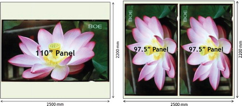
Table 1. Specific parameters of the 97.5- and 110-inch panels.
3. Panel fabrication process and panel architecture
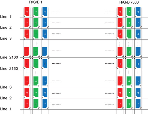
Discussed above are the panel architecture and fabrication process for an ultra-large LCD panel with ADSDS technology [Citation4]. To achieve a sufficient pixel charging ratio, the same as the 110-inch panel developed by these authors, the tried and tested a-Si thin-film-transistor (TFT) fabrication process combined with a 0.08 Ω/□ low-sheet-resistance metal, Al, was chosen for the 97.5-inch panel instead of the oxide TFT and Cu fabrication process. schematically illustrates the panel architecture of the newly developed LCD panel. The data lines are separated in the panel center, realizing the simultaneously driving of the upper and lower segments of the panel. It can also be seen that the source line system has a double source line structure (also called a “2G2D structure”), meaning its two lines can be charged simultaneously [Citation6]. By employing these techniques, the pixel LC charging time is extended to 14.8 us, and its charging ratio reaches up to 99.5%. Especially, the charging time is four times longer than that of the conventional panel architecture, where one line from one side is charged within one panel.
Figure 2. Schematic panel architecture with the data line separate in the panel center, and a 2G2D structure.
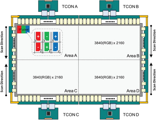
schematically depicts the panel architecture driven with a quad timing controller (TCON). The four display areas (A, B, C, and D) in the panel are driven by four TCON boards, and each of the TCON boards is assigned to one of the four display areas. In this architecture, the area of the display controlled by each TCON board is equivalent to that on a 4 K × 2 K panel. To improve the moving image quality in this architecture, the data timing between the upper and lower segments was converted. That is, the scan directions were simultaneously set to inner from outer or to outer from inner. As a result, the pixels near the separate data line area belonging to either the upper or lower segment can be charged or discharged simultaneously. Otherwise, there will be a timing interval differential of 16.7 ms, which will result in a moving image broken due to LC response unsychronization.
Figure 3. Schematic panel architecture driven with quad TCONs.
According to the panel architecture described above, the numbers of source chips on the film (COF) comprising a 1440ch output, and of the gate-COF comprising a 270ch output, are double. In the result, a total of 96 COF units are mounted at a high density on both sides of the panel. The total COF units are slightly more than those in the developed 110-inch panel [Citation4]. The COF specifications can be seen in .
Table 2. COF specifications used in the 97.5-inch panel.
4. Multi-functional image-processing video board
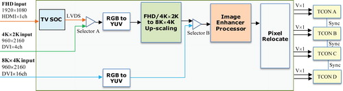
As 8 K × 4 K contents have not spread wide, it is advisable to develop a video board with multi-functional image processing supporting the data inputs of popular video formats, such as FHD or 4 K × 2 K. The key techniques consist of image upscaling and synchronization driving. These authors have successfully developed a multi-functional image-processing video board seen in , and shows a block diagram of the multi-functional image-processing video board. Several definition signals, such as FHD, 4 K × 2 K, and 8 K × 4 K, can be inputted to such video board. The FHD signal is inputted by 1ch HDMI interface, followed by LVDS format conversion in the TV system on chip board. The 4 K × 2 K signal is divided into four blocks, and the resolution of each is 960 × 2160. The signal is directly inputted by 4ch DVI (digital video interface). Selector A can automatically identify the input signal definition. Both the FHD and 4 K × 2 K signals need to be scaled by upscaling block. RGB to YUV work as a function of color space conversion. The 8 K × 4 K signal can be directly inputted through 16ch DVI, and the resolution of each channel is 960 × 2160. The signal is inputted to the image enhancer processor block and is judged by Selector B. The image enhancer processor block helps in image quality improvement, color management, and γ-correction. The pixel relocate block works to re-arrange the input data signals. Finally, the signals are divided into four parts, and each of them is sent to its TCON via the V-by-One (V × 1) connector. The sync signals for each TCON are connected to maintain synchronization.
Figure 4. Picture of the developed video board.
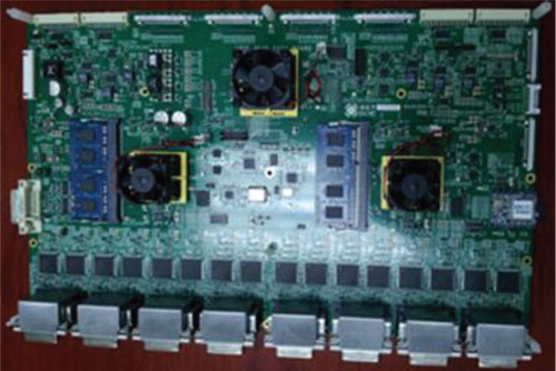
Figure 5. Block diagram of the multi-functional image-processing video board.
5. Arcing issue and solution
As discussed above, the 97.5-inch glass layout realizes the maximum glass efficiency for the ultra-large panel. That means the two panels' interval will be very small. Considering the deposited film thickness uniformity near the glass peripheral, a guaranty distance to the glass edge for the designed pattern is necessary. Thus, in the array mask design, the shield bar design is adopted, but the shield bar area in the mask will also cause the corresponding pattern residue area. To remove this pattern in such area, the edge exposure (EE) process must be available, but part of the pattern cannot be taken away due to poor EE accuracy. Unfortunately, in this study, during the half-tone source–drain mask etching process, serious arcing happened. (a) and (b) shows the arcing images under a macroscope and a microscope, respectively. It can be seen that there are large-area patterns burning on the glass. Fortunately, by improving the exposure process, this issue was finally resolved.
Figure 6. Pictures of arcing during half-tone source–drain pattern etching. (a) Arcing picture under a macroscope, (b) Arcing picture under a microscope.
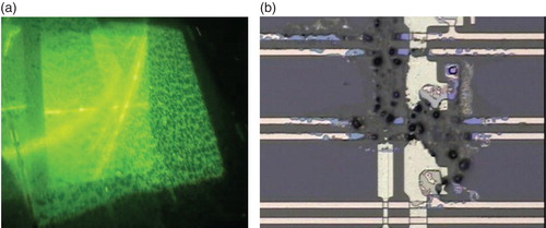
Arcing, as used here, refers to the local events that occur in the induced couple plasma reactive ion etching (ICP RIE) chamber that are detrimental to the TFT device. It is explosive, causing high-power-density short circuit in the glow discharge plasma area consisting of high-energy and secondary electrons. When it occurs on the surface of a glass substrate to which metal films have been deposited, it will result in local melting, as seen in . Based on the results of the analysis that was conducted, it can be concluded that the large-area residual metals disturb the glow discharge plasma electrical field. A uniform electric-field gradient is necessary to prevent an impact on arcing formation [Citation7,Citation8].
6. Conclusion
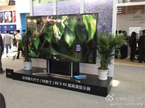
A 97.5-inch LCD panel with a 8 K × 4 K resolution was successfully developed, and its prototype can be seen in [Citation9]. This is currently the world's biggest panel size for SHV. An improved fabrication process and a driven architecture were adopted to ensure a high pixel charging ratio. The developed multi-functional image-processing video board makes it easy to match the input data resolution from FHD to 8 K × 4 K; thus, its application field for the SHV panel is extended. Fortunately, the arcing issue was solved, and an ultra-high-quality image display was realized. The panel features a 1200:1 contrast ratio, 500 nit brightness, and 72% color gamut.
Figure 7. Prototype 97.5-inch 8 K × 4 K LCD panel.
Funding
The authors gratefully acknowledge the support of the Development Fund of Beijing Talented [grant number 2011D001146000002] and the National Natural Science Foundation of China [grant numbers 51372016 and 61275022] for this research.
Additional information
Yanping Liao received his B.S. in Optoelectronics degree from Jilin University in 1998, and his M.S. (2004) and Ph.D. (2007) in Condensed Physics degrees from Changchun Institute of Optics, Fine Mechanics, and Physics, Chinese Academy of Sciences. At present, he is a postdoctoral student engaging in the study of large high-definition TV display key technologies in Beijing Jiaotong University and Beijing BOE Display Technology Co., Ltd.
Xibin Shao received his Ph.D. degree from Changchun Institute of Optics, Fine Mechanics, and Physics, Chinese Academy of Sciences in 1998. He then worked in the same institute as a professor, and also as a research fellow in Tohoku University. He is also a guest professor of Beijing Jiaotong University and is vice president of BOE Group, taking charge of IT/TV product development. He has been engaging in the study of display technologies for more than 20 years. He has led his team to successfully develop the 120Hz 4 K 110″ LCD TV, the largest LCD TV in the world, and the 98″ 8 K LCD TV. To date, he has published more than 60 papers on the LCD field, and has registered more than 100 patents.
Jianfeng Yuan is presently working in the Process Development Department of Beijing Display Technology Co., Ltd., as an expert. He received his Ph.D. in Condensed Physics degree from Changchun Institute of Optics, Fine Mechanics, and Physics, Chinese Academy of Sciences in 2004. His main interests are device processes related to AMLCD, a-Si TFTs, and organic TFTs.
Xiqing Zhang received his Ph.D. degree from Changchun Institute of Optics, Fine Mechanics, and Physics, Chinese Academy of Sciences in 1995. He joined Beijing Jiaotong University in 1997 and is now a professor engaging in ultraviolet photodetectors and thin-film-transistors.
Ji Zhang received his B.S. in Electrical Science Engineering degree from Nankai University in 2006, and is now a senior engineer and in charge of LCD module development.
Changlin Leng received his B.S. in Mechanical Engineering and M.S. in Electrical Engineering degrees from North University of China in 2000 and 2003, respectively, and his Ph.D. in Optical and Electrical Engineering degree from Tianjin University in 2006. Since 2006, he has been with BOE Technology Group Co., Ltd. and has been working on circuit driving for application to the TFT-LCD, AM-OLED, and flexible TFT. Also, he is interested in system solutions for 8 K display applications.
Yinglong Huang received his B.S. and M.S. in Physics degrees from Jilin University in 2003 and 2006, respectively, and his Ph.D. degree from the Institute of Semiconductors, Chinese Academy of Sciences in 2006. He is currently with BOE Technology Group Co., Ltd. and has been researching on the GOA, 8 K display, and oxide thin-film-transistor technology areas.
Seongkyu Lee received his Ph.D. and M.S. in Electrical Engineering degrees from Seoul National University in Korea in August 1994. For 14 years since September 1994, he has been with the LCD Division of Hyundai Electronics. He transferred to BOE Technology Group Co., Ltd. in April 2006, where he became the manager of the Product Development Department. He is currently the chief of Product Development Center for large-area LCD products. He is also a member of SID.
References
- T. Kumakura, M. Shiomi, S. Horino, Y. Yoshida and S. Mizushima, SID 2012 Digest. 43, 780 (2012).
- K. Ishii, T. Usui, Y. Murakami, Y. Motoyama, M. Seki, Y. Noguchi, T. Furutani, T. Nakakita and T. Yamashita, SID 2012 Digest. 43, 71 (2012).
- L. Vermaele, editor, The Super Hi-Vision demos at IBC-2008. EBU Tech. Rev. ( January, 2009).
- Y. Liao, X. Shao, Y. Du, Y. Song, W. Hu, Z. Zhang, Y. Chen, Y. Wang, Q. Ma, D. Yoon, D. Wang, J. Yuan, H. Wu, Z. Guo, Z. Hao, J. Zhang and J. Lv, J. Inf. Disp. 15 (2), 77–80 (2014). doi: 10.1080/15980316.2014.907214
- L. Chen, Y. Chen, H. Hou, Y. Mo and C. Chiu, SID 2013 Digest. 44, 100 (2013).
- N. Gong, C. Park, J. Lee, I. Jeong, H. Han, J. Hwang, J. Park, K. Park, H. Jeong, Y. Ha and Y. Hwang, SID 2012 Digest. 43, 784 (2012).
- L.T. Lamont Jr., Varian Vac. Views 9 (3), 2 (1975).
- L.T. Lamont Jr., J. Vac. Sci. Technol. 14, 122 (1977). doi: 10.1116/1.569101
- Nikkei Technology. <http://china.nikkeibp.com.cn/news/flat/68513-20131119.html>.