
Abstract
An electron-beam-induced crystallization technique for amorphous silicon (a-Si:H) thin films was investigated. The high-energy electron beams (e-beams) transfer their energy to the silicon network, resulting in network relaxation and crystallization. The crystalline properties of the silicon film strongly rely on the e-beam exposure time and the acceleration voltage. The crystallinity of the silicon film depends on the a-Si:H growth method used. Silicon films with higher crystallinity can be obtained from thin films deposited via plasma-enhanced chemical vapor deposition (PECVD) rather than from thin films deposited via sputtering. The PECVD silicon thin film showed more than 94% crystallinity and a ∼50 nm grain size after e-beam exposure with 1500 V acceleration bias for 180 s.
1. Introduction
There are many devices that use silicon materials, and many studies have been conducted to improve the properties of such materials. Polycrystalline silicon has better switching properties than amorphous silicon (a-Si:H) due to the former's higher electron mobility [Citation1]. Amorphous oxide thin-film transistors (TFTs) have shown high mobility, but they are still not popular and widely used due to their low stability against bias illumination stress [Citation2,Citation3]. There have been many researches on the crystallization of a-Si:H thin films, such as through rapid thermal annealing, metal-induced crystallization, and solid-phase crystallization [Citation4–6], but these techniques require high temperatures, longer process times, and expensive equipment, and have higher process costs. In addition, the orientation of crystals and the uniformity of crystallized films have yet to satisfy the needs of devices [Citation7,Citation8]. Crystallization of doped films using an electron beam (e-beam) exposure technique has been used for the activation of the ion-implanted source–drain region of the field effect transistor [Citation9]. The e-beam process can provide better opportunities for the device application of polycrystalline silicon, such as for TFT technologies [Citation10–12]. It has many advantages, such as being a lower temperature process, having lower equipment cost, and allowing easier control of the process parameters and faster processing compared to the conventional technologies [Citation13,Citation14].
The generation of uniform e-beams is one of the key parameters for the aforementioned crystallization process. In this study, electrons were extracted from a plasma source. Argon plasma was generated through an inductively coupled plasma gun system, extracted through a high-voltage mesh, and then placed on a substrate.
2. Experiments
The crystallization mechanism was studied through the e-beam exposure of a-Si:H thin films and the dehydrogenation effect of thermal annealing. In this research, two types of a-Si:H thin films were prepared, one deposited via plasma-enhanced chemical vapor deposition (PECVD) and the other via sputtering [Citation15]. The a-Si:H thin films deposited via PECVD were deposited at 360°C with SiH4 and H2 gases, while the a-Si:H thin films deposited via sputtering were deposited at room temperature with argon gas. All the a-Si:H thin films were 300 nm thick. After deposition, the films were mounted onto the e-beam exposure system. The exposure process was carried out at room temperature. The crystallization property was found to be strongly related to various process conditions, such as the RF power, DC voltage, exposure time, and properties of a-Si:H thin films.
and show the schematic diagram of the e-beam system as well as the standard e-beam exposure conditions that were used for the experiment in this study. An electron gun was positioned 60 mm above the thin-film materials, and the diameter of the e-beam mesh was 60 mm. Thus, the a-Si:H thin films were exposed to e-beams in an area with a diameter larger than 60 mm, without a scanning and focusing process. For plasma generation, 3 sccm argon gas and 300 W (∼10 W/cm2) RF power were used. The RF power is a very important parameter for the electron density in the plasma. The electrons in the plasma are accelerated though direct current bias voltage in the gun. In this process, the substrate is earthed to the ground. The electron mean free path depends on the process pressure of the chamber. In this study, the process pressure was kept at 3.0 × 10⁻⁴ Torr, and the electrons were exposed at room temperature.
Figure 1. Schematic diagram of the e-beam system.
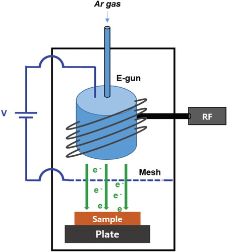
Table 1. Electron beam exposure conditions.
Argon plasma can generate a high-energy e-beam through the high DC bias on the mesh grid. The electrons extracted from an electron gun with high kinetic energy reach the substrate and convert their kinetic energy to thermal energy and transfer it to the substrate. The network vibration induced from the collisions can realize network relaxation and structural modification, resulting in a new bonding as a crystalline structure [Citation16].
The thermal annealing that was done to investigate the effect of dehydrogenation was done at 500°C for 1 h. The a-Si:H thin films with and without thermal annealing were compared after e-beam exposure.
The changes in the structural properties of the a-Si:H thin films after e-beam exposure were investigated through dark conductivity measurement, Raman spectroscopy (Jobin-Yvon, LabRam HR), X-ray diffraction (XRD; PANalytical, X'Pert PRO), Fourier transform infrared spectroscopy (Shimadzu, UV-3101PC), scanning electron microscopy (SEM; Hitachi, S-4700), and atomic force microscopy (AFM; Park System) [Citation17].
3. Results
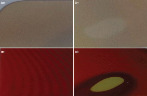
During the e-beam exposure process, the modification of the a-Si:H thin films could be observed with the naked eye, through the window in the process chamber. Based on the process conditions, no change in color was observed in the non-crystallized film, and a mild-red color change was observed in the crystallized film. The origin of the change in color during the crystallization process needs to be clarified.
shows the color change of the a-Si:H thin film after e-beam exposure. Two a-Si:H film substrates deposited via (a) sputtering and (c) PECVD, respectively, were used. The photograph images of the sputter-deposited and PECVD silicon thin films after e-beam exposure are shown in (b) and (d), respectively. The exposed region can be easily distinguished. The color of the a-Si:H thin film was changed by e-beam exposure. In the low-energy regime, a-Si:H changed its color from brown to black, and in the high-energy regime, from brown to yellow. It can be supposed that the color change was caused by the transition of the a-Si:H thin-film structure to crystalline after e-beam exposure.
Figure 2. Images obtained before and after the e-beam exposure of the a-Si:H thin films deposited via PECVD and sputtering: (a) sputter-deposited a-Si:H thin film; (b) sputter-deposited silicon thin film after e-beam exposure; (c) PECVD a-Si:H thin film; and (d) PECVD silicon thin film after e-beam exposure.
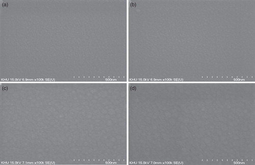
The structural properties of the e-beam-exposed samples were inspected via SEM, XRD, and Raman spectroscopy. shows the SEM images of the sputter-deposited and PECVD silicon thin films after e-beam exposure with and without thermal annealing. A grain size of tens of nanometers was obtained in the PECVD silicon thin films; on the other hand, a low level of crystallization occurred in the sputter-deposited silicon thin films. Thus, it can be seen that crystallization was better in the PECVD a-Si:H thin films than in the sputter-deposited a-Si:H thin films. The difference between the two kinds of films lies in their hydrogen content. The hydrogen contents of the PECVD and sputter-deposited a-Si thin films, as determined via infrared spectroscopy, were 15.3% and 0.5%, respectively. On the other hand, there were minimal differences in grain size between with and without thermal annealing in the sputter-deposited and PECVD silicon films.
Figure 3. SEM images of the silicon thin films after e-beam exposure: (a) sputter-deposited silicon thin film; (b) sputter-deposited silicon thin film with thermal annealing; (c) PECVD silicon thin film; and (d) PECVD silicon thin film with thermal annealing.
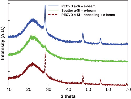
shows the XRD patterns of the samples. Strong peaks can be seen at 2θ = 28.4°, 47.3°, and 56.1° in the PECVD silicon thin film, which correspond to the (111), (220), and (311) crystal planes of silicon and certify the crystalline structure of the silicon thin films [Citation18]. On the other hand, very weak crystalline peaks can be seen in the sputter-deposited silicon thin film.
Figure 4. XRD patterns of the silicon thin films after crystallization via e-beam exposure.
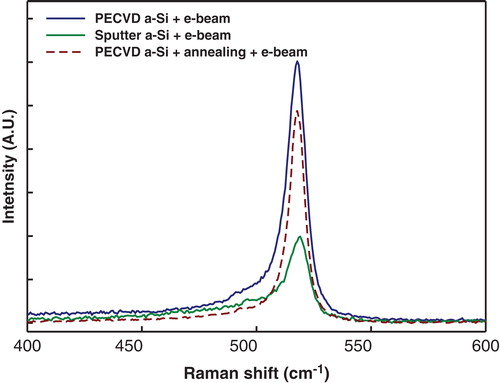
shows the Raman spectra of the e-beam-exposed a-Si:H thin films. Almost no amorphous peaks near 480 cm−1 were shown in the PECVD and sputter-deposited silicon thin films. The a-Si:H thin film deposited via PECVD showed a strong crystalline spectrum after e-beam exposure. The sputter-deposited silicon thin film also showed a crystallization peak, but the crystallization fraction was smaller than those of the PECVD samples.
Figure 5. Raman spectra of the silicon thin films after crystallization via e-beam exposure.
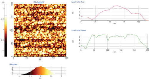
shows the AFM image and roughness of the PECVD a-Si:H thin film after crystallization via e-beam exposure. The root mean square roughness and average roughness were 2.265 and 2.23 nm, respectively. The surface roughness of the silicon thin film crystallized via e-beam exposure was completely smooth compared with the silicon thin films crystallized using other crystallization processes, for the active layer of devices. Electrons interact with one another through the electrostatic force, resulting in a uniform spatial distribution and a smooth surface.
Figure 6. AFM image and roughness of the PECVD silicon thin film after e-beam exposure.
4. Discussion
E-beam processes have been investigated for annealing semiconductor materials that have sustained ion-implanted damage, and for growing nanostructure layers. In this study, the crystallization mechanism of the a-Si:H layer via e-beam exposure was investigated.
To determine the causes of the differences in crystallinity between films, a PECVD a-Si:H thin film was annealed at 500°C for 1 h for dehydrogenation, after which it was exposed to an e-beam under the same conditions. The hydrogen in the PECVD a-Si:H thin film was eliminated via annealing. The hydrogen content of the annealed PECVD a-Si:H thin film, as determined via infrared spectroscopy, was 0.7%, which is similar to that of the sputter-deposited a-Si:H thin film. It was assumed that if hydrogen is a dominant factor for crystallization, the a-Si:H thin film dehydrogenated via annealing and crystallized via e-beam exposure should show the same XRD and Raman spectrum as the sputter-deposited a-Si:H thin film crystallized via e-beam exposure. As shown in , however, the a-Si:H thin film annealed at 500°C and then exposed to an e-beam had the same diffraction peak (dashed line) as the e-beam-exposed PECVD a-Si:H thin film without annealing. Moreover, the same trend appeared in the Raman spectrum, as shown by the dotted line in . Based on these measurement results, it can be said that the crystallization of a-Si:H depends on the growth method used rather than on the hydrogen content of the a-Si:H thin film. It seems that the sputter-deposited a-Si:H thin film has a higher defect density, and that its defect state reduces the network vibration, resulting in less opportunities for crystallization. More energy exposure is needed for the crystallization of sputter-deposited films, to overcome the binding energy of the defect state. The acceleration voltage required in the process of e-beam exposure is more than 1500 V, but the acceleration voltage of the proposed system is limited to 1500 V.
From the Raman spectrum, the crystalline volume fraction can be calculated with the deconvolution of the spectrum. The crystalline volume fraction was obtained from [Citation19,Citation20]:
(1)
where, Ia, Ic, and Im are the intensities of the amorphous (480 cm−1), crystalline (520 cm−1), and intermediate (500–510 cm−1) peaks, respectively. The PECVD silicon thin film showed more than 94% crystallinity and 6.0 cm−1 full width at half maximum (FWHM) after e-beam exposure with 1500 V acceleration bias for 180 s. In the case of the PECVD a-Si:H thin film with thermal annealing, the crystallinity and FWHM were 90% and 7.2 cm−1, respectively. The sputter-deposited silicon thin film, however, showed 77% crystallinity and 10.3 cm−1 FWHM. Therefore, the sputter-deposited silicon thin film showed lower crystallinity than the PECVD silicon thin film. For high-performance devices, the crystallinity of sputter-deposited silicon thin films should be improved through the optimization of the e-beam exposure conditions.
The structural modification of the a-Si:H thin film was achieved via e-beam exposure for 180 s. It was found that the crystalline properties strongly depend on the growth method used rather than on the hydrogen content of the a-Si:H thin film. The sputter-deposited a-Si:H thin film with a higher defect density showed poorer crystalline properties than the PECVD a-Si:H thin film. Considering the a-Si:H growth method, the silicon thin film crystallized via e-beam exposure could be applied to the device fabrication process. The a-Si:H sputter deposition technique is important for flexible display device fabrications. With the e-beam exposure technique, sputter-deposited a-Si:H thin films could be crystallized, but their performance would not be competitive with that of the PECVD a-Si:H thin films. To apply sputter-deposited thin films to flexible devices, additional studies are needed to find a more evident crystallization mechanism.
5. Conclusion
The structural modification of amorphous silicon (a-Si:H) thin films via e-beam exposure was investigated. Through SEM, XRD, and Raman spectroscopy, it was found that the crystallization characteristics are affected by the deposition method used rather than by the hydrogen content of the a-Si:H thin film, and that e-beam exposure could modify the network of a-Si:H thin films, and then crystallization can occur. In the case of the a-Si:H thin film deposited via PECVD, more than 94% crystallinity was obtained via Raman measurement after e-beam exposure. This method is a relatively simple process and has a shorter process time. It is expected that the silicon thin film crystallized via e-beam exposure will be used in the device fabrication process.
Additional information
Funding
Byeong-Yeon Moon received his B.S., M.S., and Ph.D. in Physics degrees from Kyung Hee University, South Korea, in 1991, 1994, and 1998, respectively. He is currently a professor at Kangwon National University, teaching optometry.
Jung Su Kang received his M.S. in Information Display degree from Kyung Hee University, South Korea, in 2014 and is currently a researcher on electron beams and field emission at Kyung Hee University.
Seon Yong Park received his B.S. in Information Display degree from Kyung Hee University, South Korea, in 2012. He is currently a researcher on semiconductor physics at EcolePolytechnique, France.
Kyu Chang Park received his B.S., M.S., and Ph.D. in Physics degrees from Kyung Hee University, South Korea, in 1990, 1993, and 1997, respectively. He worked for Hyundai from 1997 to 2002. Since 2002, he has been a professor at Kyung Hee University, teaching information display.
References
- T. Sameshima, M. Hara and S. Usui, Jpn. J. Appl. Phys. 28, 1789 (1989). doi: 10.1143/JJAP.28.1789
- H. Ohshima, Jpn. J. Appl. Phys. 53 (3S1), 03CA01 (2014). doi: 10.7567/JJAP.53.03CA01
- S.H. Kim, K.S. Jeong, G.W. Lee and H.D. Lee, J. Inf. Disp. 14, 61 (2013). doi: 10.1080/15980316.2013.802749
- M. Miyasaka and J. Stoemenos, J. Appl. Phys. 86, 5556 (1999). doi: 10.1063/1.371560
- R. Kakkad, J. Smith, W.S. Lau, S.J. Fonash and R. Kerns, J. Appl. Phys. 65, 2069 (1989). doi: 10.1063/1.342851
- T. Pier, K. Kandoussi, C. Simon, N. Coulon, T. Mohammed-Brahim and H. Lhermite, J. Non-Cryst. Solids 354, 2300 (2008). doi: 10.1016/j.jnoncrysol.2007.10.087
- K.C. Park, J.H. Lee, I.H. Song, S.H. Jung, and M.K. Han, J. Non-Cryst. Solids 299–302, 1330 (2002). doi: 10.1016/S0022-3093(01)01097-3
- K. Nakazawa, J. Appl. Phys. 69, 1703 (1991). doi: 10.1063/1.347215
- T.B. Peters, M.B. Pitt, R.A. Mcmahon, D.G. Hasko and H. Ahmed, IEEE Electron Dev. Lett. 6, 482 (1985). doi: 10.1109/EDL.1985.26200
- R.A. McMahon, D.G. Hasko and H. Ahmed, Rev. Sci. Instrum. 56 (6), 1257 (1985). doi: 10.1063/1.1137987
- H. Ishiwara and K. Suzuki, Jpn. J. Appl. Phys. 23, 1065 (1984). doi: 10.1143/JJAP.23.1065
- A.G. Gullis, Rep. Prog. Phys. 48, 1155 (1985). doi: 10.1088/0034-4885/48/8/002
- Y.J. Jo, C.H. Hong and J.S. Kwak, Curr. Appl. Phys. 11, S143 (2011). doi: 10.1016/j.cap.2011.03.082
- C.W. Byun, S.W. Son, Y.W. Lee and S.K. Joo, Electron. Mat. Lett. 8, 251 (2012). doi: 10.1007/s13391-012-2079-x
- J. Jang, K.M. Kim, K.S. Cho, B.K. Choo and G. Um, IEEE Elec. Div. Lett. 24, 78 (2003). doi: 10.1109/LED.2003.808838
- S. Johnson, A. Markwitz, M. Rudolphi, H. Baumann, S.P. Odi, K.B.K. Teo and W.I. Milne, Curr. Appl. Phys. 6, 503 (2006). doi: 10.1016/j.cap.2005.11.049
- Q. Cheng, S. Xu, and K. Ostrikov, Nanotechnology 20, 215606 (2009). doi: 10.1088/0957-4484/20/21/215606
- U.K. Das, P. Chaudhuri and S.T. Kshirsagar, J. Appl. Phys. 80, 5389 (1996). doi: 10.1063/1.363481
- D. Song, D. Inns, A. Straub, M.L. Terry, P. Campbell and A.G. Aberle, Thin Solid Films 513, 356 (2006). doi: 10.1016/j.tsf.2006.01.010
- Guozhen Yue, J.D. Lorentzen, Jing Lin, Daxing Han and Qi Wang, Appl. Phys. Lett. 75, 492 (1999). doi: 10.1063/1.124426