
ABSTRACT
Portable models based on the latest liquid crystal displays (LCDs) have been useful in various areas. Many developers have pursued thinner hardware as well as the advanced performance of portable models. Therefore, as the panel glass continuously becomes thinner, the strength characteristics of glass are highlighted as an important issue. In particular, the strength of the LCD glass is mentioned as an important issue. The occurrence of surface scratches on the active-matrix liquid crystal display glass substrates should be minimized to produce portable models with stability; if their crack flaw sizes are kept below a certain level or close to zero, strength-differentiated LCD panel production will be possible. This study confirmed that in LCD panels where the thin-film transistor-color filter (TFT-CF) is assembled, cracks are generated mainly in the TFT glass, and the mirror constant is at a 60.038 MPaċmm0.5 level. In addition, this suggests that the size of the crack flaws that may occur on the glass surfaces during the LCD process should be minimized to produce panels that can withstand a certain impact level through the fracture surface analysis of the glass crack origins.
1. Introduction
Studies on the crack occurrence on the active-matrix liquid crystal display (hereinafter, ‘AMLCD’) glass substrates have been continuously conducted, and various data have been reported. In the final glass substrates that become products in practice, however, several factors during the liquid crystal display (hereinafter, ‘LCD’) process change the material properties of the substrates and have a decisive effect on the fracture stress depending on the management of the flaws on the substrate surfaces when the panel cracks occur. In particular, the microscratches that occur on the glass surfaces during the LCD panel production become the crack origins in the panels; the degree of stress that causes the glass to be destroyed changes in accordance with the flaw size. The cracks in LCD panels primarily occur in the thin-film transistor (hereinafter, ‘TFT’) glass because the TFT process involves a relatively larger number of steps compared to the color filter (hereinafter, ‘CF’) process, thereby being much more disadvantageous in terms of the occurrence of surface scratches. The present study conducted the four-probe bend test to determine the mirror constant of the LCD panel glass from the completed process; a ball drop test was also conducted to generate glass cracks in the active area of the LCD panels. Moreover, the results were observed using an optical microscope (SEC-2000) to determine the fracture dimensions and the forms of the crack origins of the samples from the completed experiment.
2. Glass crack origin analysis methods
2.1. Crack branch
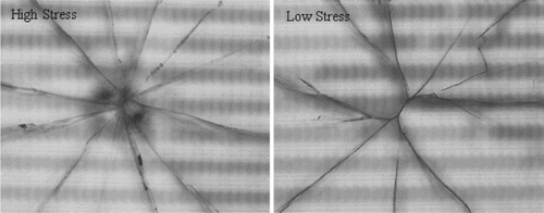
The principle of glass crack generation is that the force generated by the externally applied stress is propagated into the surfaces and interior of the glass from the crack origin, like a branch. The intersection of each branch represents a point where the force is propagated. Although glass cracks seem to have complex forms, it is possible to identify the crack origin when a trace of the branch through which the force is transmitted is found. As shown in Figure , the stronger the externally applied stress, the greater the number of crack branches. This phenomenon shows that the force due to the strong stress at the crack origin is propagated in many ways [Citation1].
Figure 1. Crack branches with high and low stress.
2.2. Fracture surface
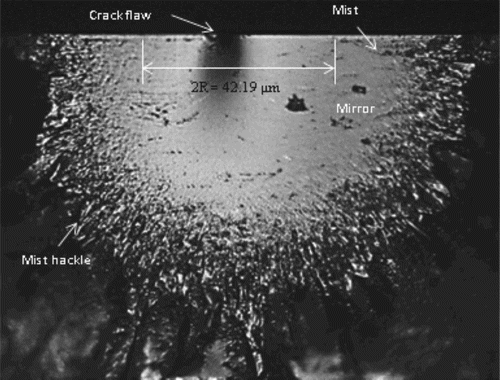
Fracture surfaces can be identified through a scope review of the cross-section of the crack origin. The fracture surfaces caused by general bending tension stress consist of crack flaws, mirrors, mist, Wallner lines, and hackles, all of which appear in the form of semicircles around the crack flaw. The corresponding parts are the traces generated by the momentary changes in the speed and size when the force by the externally generated stress is propagated to crack branches other than the crack origin. In addition, the corresponding parts are important elements that indicate the magnitude of the external force where cracks occurred. The fracture surface dimensions depending on the magnitude of the externally generated stress are shown in Figures –.
Figure 2. Fracture surface I (mirror radius (R) = 95.265 µm; fracture stress = 194.52 MPa).
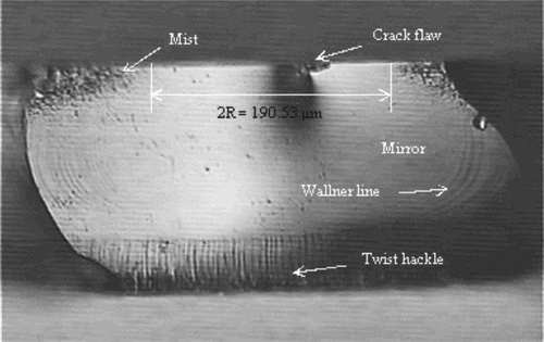
Figure 3. Fracture surface II (mirror radius (R) = 39.595 µm; fracture stress = 301.72 MPa).
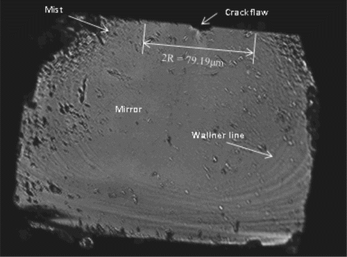
Figure 4. Fracture surface III (mirror radius (R) = 21.095 µm; fracture stress = 413.37 MPa).
2.3. Crack flaw, mirror
Pure glass without scratches has a significantly higher strength compared to other materials. The main reason for crack occurrence in glass following an impact is the force from the stress acting on the crack flaws, such as the glass surface scratches or glass edge ripples. Although it is difficult to observe crack flaws with the naked eye, in some cases, crack flaws less than or equal to ∼1.00 µm can be viewed using a microscope. All the elements identified on the fracture surfaces exist in the form of semicircles around the crack flaws, with each element held in position in the semicircle composition, like the planets.
Mirror areas exist in close proximity to crack flaws. Mirrors exist between crack flaws and hackles, and are the most important factor in crack analysis. Through the measurement of the mirror radius shown in Figures –, it is possible to predict the acting fracture stress. Mirrors are the areas generated when the velocity of the force propagated from the crack flaws temporarily becomes low. The sizes of their areas change depending on the magnitude of the acting external pressure. The stronger the generally acting tension stress, the narrower the mirror areas near the crack origin. Conversely, the weaker the tension stress, the wider the areas. As the stronger the force, the faster the propagating speed in general, this result shows that the changes in the sizes of the mirror areas at the crack origin are caused by the velocity of the force propagated from the crack flaws.
2.4. Wallner line, mist, hackle
When forces, such as cutting, rolling, and pressing, and fine vibrations act uniformly on the substrate surfaces of materials at the same time, chatter marks arise thereon. This phenomenon appears in every material, such as glass, metals, PVCs, trees, and stones (by glacier). If fine vibrations occur while the force is propagated by the tension stress from the crack flaws to the areas right in front of the hackles, dense Wallner lines occur on the mirror surfaces. As shown in Figure , the lower the fracture stress is, the more clearly Wallner lines appear. This is because the velocity decreases momentarily in the process of force propagation by the external impact so that the number of times that fine vibrations acted in the vicinity of the cracks increases within the same time. In fact, as shown in the fracture images in Figures –, the weaker the acting bending stress is, the more vivid the Wallner lines become, and the greater the increase in their number.
During glass crack generation, the velocity of the crack propagation that progresses slowly from the crack flaws to the mirror areas increases momentarily; at this moment, mists and hackles are created. As shown in the fracture images, the hackles have relatively rougher surfaces, and their boundaries are more evident than those of the mists. In particular, the distance between the mists and the crack flaws represents the mirror radius, which is an important factor that must be considered in estimating the magnitude of the fracture stress acting on the crack origin. As shown in Figures and , the hackles can be classified into mist hackles and twist hackles depending on the magnitude of the fracture stress. The mist hackles arise around the crack origin under a strong bending stress while the twist hackles arise in the direction in which the glass is bent under a relatively weak bending stress.
2.5. Mirror radius and mirror constant
The distance between the crack flaws and the mists is the mirror radius. Mirror radius R varies depending on the magnitude of σ, which is the fracture stress acting on the crack origin, and can be defined as follows [Citation2,Citation3]:
where A is the mirror constant. In the previous study, the value that was obtained when the 0.7- and 1.1-mm-thick and 50 × 50-mm Code 1737 AMLCD glass substrates (alkaline-earth boroaluminosilicate glass) were measured was 65.3 ± 0.4 MPa·mm0.5 [Citation4]. In particular, the corresponding results demonstrated that the mirror constant of glass does not change even if the glass thickness is different. The results, however, are the values for bare glass substrates; unlike bare glass, the AMLCD glass that actually undergoes a number of processes has residual stress. The relational expression including residual-stress constant Δσ0 is defined as shown below [Citation5]:
3. Experiment procedure and results
3.1. Four-probe bend test
When glass cracks occur, the magnitude of the fracture stress can be determined through the four-probe bend test. Basically, the structure and equation of the four-probe bend test equipment are as shown below [Citation6] (Figure ):
Figure 5. Four-probe bend test.
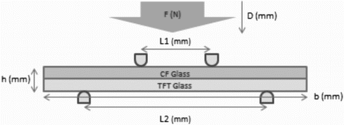
In the equation above, F is the force applied to loads L2 and L1, h is the thickness of the test sample, and b is the x-axis distance of the test sample. K is a comparison factor and is normally found in the range of 1.5–1.7 based on the experiment results. The K value that was used in the corresponding experiment was 1.6. The size of the test sample that was used in this study was 270 × 206 mm, and the total thickness was 0.4 mm. The samples underwent TFT–CF assembly and cell scribe. Load L1 was 25 mm, and load L2 was 50 mm.
Bending stress was exerted between edge points L1 and L2 by force F; as a result, cracks occurred at the crack origin that was present in the scribe cutting line. In the corresponding experiment, the ripples present in the cut glass edge became the crack origins. The fracture surface of the crack origin in the sample in which cracks occurred was found, and its mirror radius was measured.
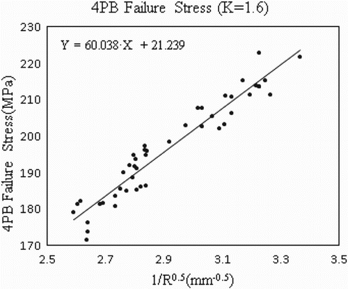
In the four-probe bend test of the LCD panels, the substrate in which cracks occurred regardless of the direction of the panels was the TFT glass; no crack was generated in the CF glass. In the panel that underwent the LCD process as shown below, mirror constant A of the TFT glass was determined to be 60.038 MPa·mm0.5 through the experiment results. In addition, it was confirmed that 21.239 MPa residual stress existed. This result demonstrated that unlike in pure bare glass, in TFT glass, various factors may lead to data scattering ().
3.2. Ball drop test
In the finished-product step, among the types of impact tests for LCD panels, the ball drop test is an important test for determining whether cracks are generated when a physical impact is applied to the pixel areas (active areas) of the products being sold in the market. In particular, it is possible to determine the magnitude of the stress applied to the interior LCD glass in terms of modules. In the ball drop test in this study, the height was adjusted up to 20–50 cm, and a steel ball weighing 150 g was dropped, resulting in cracks on the panel (Figure ).
As a result of the experiment, cracks occurred in the TFT glass, as shown in the four-probe bend test. After confirming the fracture surfaces of the crack origin, crack flaws with diverse sizes were detected thereon; mirrors, mists, Wallner lines, and hackles, all of which were generated as if drawing circles around the surfaces, were observed. The jig part at both edges of the LCD panel became the support, and the part where the ball dropped became the central part where the force acted. The bending stress generated cracks by acting on the pixel areas of the LCD panel.
In addition, the crack origin was found at the back surface (without any pattern) of the TFT glass. This was because the TFT glass back surface was vulnerable to microscratches because it made the most contact with the equipment unit between the processes. After confirming the crack flaws, mirror radius, and fracture stress on the fracture surface of the TFT glass where cracks occurred, the results shown in were observed.
Table 1. Measurement and calculation results according to the ball drop test.
4. Discussion
From Figure , it was confirmed that mirror constant A of the TFT glass of the corresponding sample was 60.038 MPa·mm0.5, which was different from that of the previously reported pure bare glass. Moreover, it was discovered in the fracture stress graph that 21.239 MPa residual stress acted on the process by which the panel glass that was used in the experiment was destroyed. In practice, the bare glass put into the process undergoes numerous deposition, etch, and heat treatment processes and passes numerous equipment units. It was found in this study that changes occur in the physical properties of glass and in the residual stress due to the impact of these processes.
Figure 6. Four-probe bend test results.
From Figures and , it was confirmed that as the length of the crack flaws increases, the fracture stress decreases. Furthermore, it was found in this study that the difference in fracture stress is reduced at more than or equal to a certain crack flaw size. Through a trend line formula, it was determined that crack flaw size C and fracture stress σ have the relational expression shown below (Figure ):
Figure 7. Ball drop test.
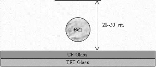
Figure 8. Ball drop test results: crack flaw vs. mirror radius.
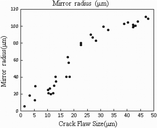
Figure 9. Ball drop test results: crack flaw vs. fracture stress.
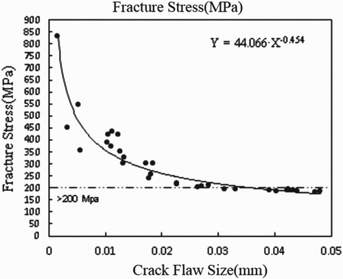
Using the above relational expression, it is possible to estimate the maximum value of the crack flaw size that should be managed between the LCD processes so that the panel produced under the conditions of the corresponding test sample can withstand the desired impact. For example, it is possible to speculate that the minimum flaw size on the glass surface that can withstand 200.07 MPa fracture stress is less than or equal to 35.72 µm.
5. Conclusion
Before smart devices gained ubiquity, LCD panels were mainly applied to stationary products, such as large TVs and monitors. Since recently, however, the portable products to which the LCD panels are applied have come to account for the majority of LCD uses in people's lives. In particular, most portable products are demanding thinner AMLCD glasses for the weight lightening of panels. Therefore, systematic research is needed so that LCD glass can be made to possess excellent strength characteristics.
The present paper proposes a way of determining the cause of crack occurrence in LCD panels, and their strength characteristics. In addition, the paper demonstrates that the panels should be managed so that scratches (crack flaws) would not occur on the glass surface between processes, so as to produce panels that can withstand a certain level of impact that occurs when using products based on the corresponding theory. If the occurrence of crack flaws on the glass surface between the LCD processes can be kept below a certain level or close to zero, it will be possible to produce strength-differentiated LCD panels.
Disclosure statement
No potential conflict of interest was reported by the authors.
Additional information
Notes on contributors

Si-jin Kim
Si-jin Kim received his B.S. Electrical and Electronic Engineering degree from Hongik University, Seoul, South Korea in 2011, and is currently a senior engineer at Samsung Display Company. He has been conducting research on the oxide-semiconductor-based TFTs, the photo alignment technology, and LCD panel crack analysis in the company.

Seung-ju Choi
Seung-ju Choi received his B.S. Material Science & Engineering degree from Hongik University, Seoul, South Korea in 2013, and is currently a senior engineer at Samsung Display Company. He has been conducting research on the LCD color filter, the photo alignment technology, and LCD panel crack analysis in the company.
References
- T. Ono and R.A. Allaire, Fracture Analysis, a Basic Tool to Solve Breakage Issues, SEMI FPD Expo Taiwan, TIP 201, 2000.
- E.B. Shand, J. Am. Ceram. Soc. 42, 474 (1959). doi: 10.1111/j.1151-2916.1959.tb13560.x
- J.J. Mecholsky, R.W. Rice, and S.W. Freiman, J. Am. Ceram. Soc. 57, 440 (1974). doi: 10.1111/j.1151-2916.1974.tb11377.x
- S.T. Gulati, J.F. Bayne, W.R. Powell and J.D. Helfinstine, Am. Ceram. Soc. Bull. 83, 14 (2004).
- D. Roberto and Z. Ricardo, J. Am. Ceram. Soc. 96, 3908 (2013). doi: 10.1111/jace.12627
- M.H. Lin, W.W. Pan, P.J. Cheng and K.F. Huang, SID Symp. Dig. Tech. Pap. 45, 697 (2014). doi: 10.1002/j.2168-0159.2014.tb00183.x