
ABSTRACT
This paper reports a comparative study of thermal stability between all-organic metal halide perovskite (MHP) CsPbBr3 and organic–inorganic hybrid MHP (methylammonium lead bromide MAPbBr3). The film morphology, crystal structure, steady-state photoluminescence intensity, and photoluminescence lifetime of CsPbBr3 and MAPbBr3 polycrystalline films were measured after thermal annealing at temperatures from 70°C to 230°C. The CsPbBr3 films exhibited little change in their structural and luminescent properties after being annealed even at 230°C, whereas the MAPbBr3 films exhibited a significant change in such properties due to their decomposition into PbBr2 when annealed at ≥180°C. This study increased the understanding of the difference in the thermal stability of MHP polycrystalline films with different A-site cations.
1. Introduction
Metal halide perovskites (MHPs) have superior optical properties, such as high photoluminescence (PL) quantum efficiency (>70% for colloidal MHP nanoparticles [Citation1–5]), narrow emission spectrum (full width at half maximum <20 nm [Citation1,Citation6]), and sharp absorption edge (low energetic disorder) [Citation7,Citation8]. Therefore, MHPs have been used in light-emitting diodes (LEDs) [Citation1,Citation6,Citation9–17] and optically pumped lasers [Citation18,Citation19]. The most representative chemical formula of MHPs is ABX3 (A is an organic ammonium, an alkali metal cation, or a mixture thereof; B is a metal cation (usually Pb2+); and X is Cl−, Br−, I−, or a mixture thereof) [Citation1]. This ternary chemical structure enables the easy tuning of the optical properties (e.g. bandgap) of MHPs by controlling the molar proportions of their constituents; therefore, the emission color of MHPs can be easily tuned from blue to infrared by adjusting the ratio of the halide anions in them [Citation10]. Also, MHPs have a much lower material cost than the conventional organic emitters (e.g. Ir(ppy)3) and colloidal inorganic quantum dot (QD) emitters (e.g. CdSe/ZnS QDs). Furthermore, various solution processes can be used to fabricate MHP layers because MHP precursors are soluble in polar aprotic solvents (e.g. dimethylformamide, dimethyl sulfoxide (DMSO)).
Since the demonstration of MHP LEDs (PeLEDs) that are bright (>100 cd m−2) at room temperature (RT) [Citation10,Citation11], the electroluminescence (EL) efficiency of PeLEDs has been significantly improved [Citation1–4,Citation6,Citation9,Citation14–17,Citation20,Citation21]. High-efficiency methylammonium lead bromide (MAPbBr3) PeLEDs (maximum current efficiency = 42.9 cd A−1) have been achieved by suppressing the formation of luminescence quenchers and using nanocrystal pinning to fabricate pinhole-free MAPbBr3 polycrystalline films with decreased grain size [Citation9]. High-efficiency PeLEDs have also been achieved using Ruddlesden-Popper phase [Citation12–15], interfacial layer engineering [Citation10,Citation21], and colloidal nanoparticles [Citation2–4]. These achievements of high-efficiency PeLEDs demonstrated the great potential of MHPs as light emitters.
Despite the dramatic progress in EL efficiency, however, the stability of MHP materials and PeLEDs must be further improved. Particularly, the thermal instability of MHPs must be overcome because it limits the applicability of high-temperature processes that are often required to fabricate MHP films with high crystallinity [Citation22]. Also, the large amount of heat generated by Joule heating or solar radiation in PeLEDs can degrade the MHP layers in them and may cause decoupling of the constituting layers at their interfaces [Citation23].
Onset temperature TDEC of thermal decomposition is lower in organic–inorganic hybrid (OIH) MHPs based on the MA+ cations (e.g. MAPbI3 and MAPbBr3) (∼220°C for MAPbBr3) than in all-inorganic (AI) MHPs (e.g. CsPbBr3; TDEC ∼ 580°C) [Citation24]; as such, OIH MHPs are more vulnerable to thermal stress than are AI MHPs. In practice, decomposition of MA-based OIH MHPs can occur at temperatures <TDEC (even at 85°C [Citation25]). Therefore, AI MHPs (CsPbX3) are promising alternative emitters for overcoming the thermal instability [Citation6]. The influences of thermal stress on the structural and optical properties of CsPbX3 polycrystalline films, however, have not been fully investigated compared with MAPbX3, especially for Br-based MHPs.
In this work, the influence of A-site cation on the thermal stability of MHPs was investigated by comparing polycrystalline films of OIH MHP MAPbBr3 and AI MHP CsPbBr3. The changes in the film morphology, crystal structure, steady-state PL, and PL lifetime were observed and analyzed at different thermal annealing temperatures (70 ≤ TANN ≤ 230°C). This study provided a better understanding of how the structural and luminescent properties of these MHP polycrystalline films change with thermal stress.
2. Experiment
2.1. Preparation of MAPbBr3 and CsPbBr3 films
CsBr (99.999%, trace metal basis), PbBr2 (≥98%), and DMSO (≥99.9%, anhydrous) were purchased from Aldrich. MABr was purchased from Dyesol. MAPbBr3 precursor solutions (40.0 wt%) were made by mixing MABr and PbBr2 in DMSO at RT while stirring (MABr:PbBr2 = 1.05 : 1, mol:mol). CsPbBr3 precursor solutions (10.4 wt%) were made by mixing CsBr and PbBr2 in DMSO at RT while stirring (CsBr:PbBr2 =1.1 : 1, mol:mol).
MHP polycrystalline films were fabricated on glass or Si native wafer/self-organized conducting polymer (SOCP) substrates using the methods described elsewhere [Citation6,Citation9]. SOCP is made of poly(3,4-ethylenedioxythiophene): poly(styrenesulfonate) (PEDOT:PSS) (CleviosTM PVP AI4083) and perfluorinated ionomer (PFI) with a PEDOT:PSS:PFI = 1:6:25.4 weight ratio [Citation9]. Thereafter, the MHP layers were annealed at 70°C, 120°C, and 180°C for 10 min or at 180°C and 230°C for 30 min in a nitrogen atmosphere.
2.2. X-ray diffraction (XRD)
The XRD patterns of the MHP films (Si native wafer/SOCP/MHP) were measured in ambient conditions at RT using an X-ray diffractometer (D/Max-2500/PC, RIGAKU) operated at 40 kV and 100 mA (scan rate = 4° min−1) to make Cu Kα radiation (wavelength = 1.54 Å).
2.3. Steady-state PL and time-correlated single-photon counting (TCSPC)
For use in steady-state PL and TCSPC measurements, the MHP films (glass/SOCP/MHP) were encapsulated with glass lids under a nitrogen atmosphere using a UV-curable resin, and were excited by 405 nm light sources. The steady-state PL of the MHP films was measured at RT using a spectrofluorometer (FP6500, JASCO). The PL lifetime of the MHP films was measured at RT using a TCSPC system [Citation2] consisting of a picosecond-pulsed laser diode head (LDH-P–C-405B, PicoQuant), a TCSPC module (PicoHarp 300, PicoQuant), a monochromator (SP-2155, Acton), and a microchannel plate photomultiplier tube (R3809U-50, Hamamatsu).
3. Results and discussion
To investigate the thermal stability of MAPbBr3 and CsPbBr3 polycrystalline films, scanning electron microscopy (SEM) was used to observe the changes in the film morphology after annealing at TANN = 70°C, 120°C, 180°C, or 230°C (Figures and ). The MHP films were fabricated on the SOCP layers to create a uniform film morphology as reported in previous studies [Citation6,Citation9]. The MAPbBr3 film without thermal annealing had a uniform fully covered morphology but also had numerous voids formed between the grains ((a)). At TANN = 70°C or 120°C, the film morphology of the MAPbBr3 films was improved; the grains were more closely packed without the voids than the grains without annealing were, and no thermal degradation was observed ((b) and (c)). At TANN = 180°C, degraded areas appeared in 10 min ((d)), and the film morphology completely changed to a non-uniform morphology with partial surface coverage in 30 min ((e)); and at TANN = 230°C, the film morphology did not further change from that of the film annealed at 180°C for 30 min ((e) and (f)), indicating that the degradation process was completed (note that the darker regions were the SOCP layers at the bottom of the MAPbBr3 layer). This degradation is ascribed to the decomposition of MAPbBr3 into PbBr2, which follows one or both of the reaction paths shown below [Citation26]:
(1)
(2)
Figure 1. SEM images of the MAPbBr3 polycrystalline films with different thermal annealing conditions: (a) without annealing; (b) annealed at 70°C for 10 min; (c) annealed at 120°C for 10 min; (d) annealed at 180°C for 10 min; (e) annealed at 180°C for 30 min; and (f) annealed at 230°C for 30 min.
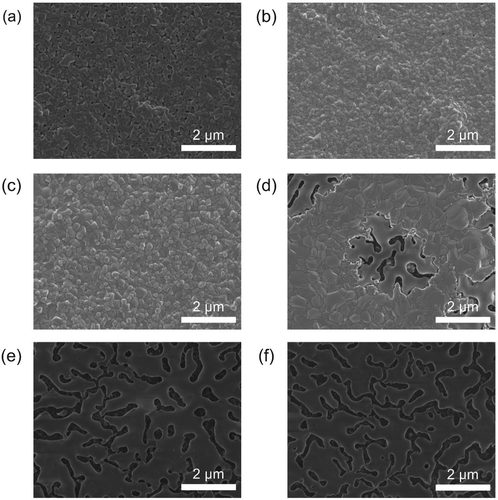
Figure 2. SEM images of the CsPbBr3 polycrystalline films with different thermal annealing conditions: (a) without annealing; (b) annealed at 70°C for 10 min; (c) annealed at 120°C for 10 min; (d) annealed at 180°C for 10 min; (e) annealed at 180°C for 30 min; and (f) annealed at 230°C for 30 min.
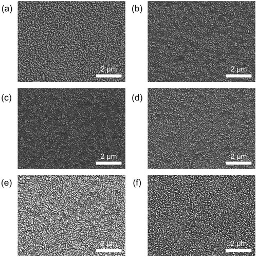
The MAPbBr3 grains were fused together with the adjacent grains during the decomposition into PbBr2. This fusing effect is a result of Ostwald ripening [Citation27] or coalescence [Citation28]; both processes can be accelerated by high annealing temperatures (TANN = 180 or 230°C) and by the methylamine gas created during the decomposition. The increase in grain size with increasing TANN (from 70°C to 180°C) can also be explained by coalescence ((b)–(d)) [Citation28]. In contrast, the CsPbBr3 polycrystalline films were thermally stable; the films annealed at 180°C and 230°C did not show any degradation in morphology (). The high thermal stability of CsPbBr3 films is attributed to (i) the absence of proton-donating organic constituents and decomposition reactions (1) and (2) and (ii) a positive enthalpy of the decomposition reaction of CsPbBr3 [Citation29].
To determine if the thermal stresses changed the crystal structures of the MAPbBr3 and CsPbBr3 films, the XRD patterns of the two MHP films with different annealing conditions were obtained (; Tables ). The MAPbBr3 film annealed at 70°C showed 4 major XRD peaks at 15.02°, 21.26°, 30.20°, and 33.86°, which can be respectively indexed as (100), (110), (200), and (210) planes in cubic Pmm phase ((a), ). The MAPbBr3 films annealed at 180°C for 30 min exhibited XRD peaks from both MAPbBr3 and PbBr2; only the (100) and (200) peaks of MAPbBr3 remained at the same positions as those in the film annealed at 70°C. This indicates that the MAPbBr3 film annealed at 180°C for 30 min was not completely decomposed into PbBr2 despite the complete change in its morphology ((b)). The application of Bragg's law determined that the lattice parameter of MAPbBr3 was 5.891 Å (). The MAPbBr3 film annealed at 230°C exhibited a completely different XRD pattern, which matches well with the calculated XRD pattern of PbBr2 ((a) and (c)) [Citation30]; this change confirms that the decomposition of MAPbBr3 was completed by annealing at 230°C for 30 min. This temperature is slightly above the TDEC∼220°C of MAPbBr3 [Citation24]. The occurrence of thermal decomposition at temperatures below the TDEC of MAPbBr3 (e.g. 180°C in this work) has often been reported [Citation25,Citation31,Citation32].
Figure 3. XRD patterns of (a) MAPbBr3 and (b) CsPbBr3 polycrystalline films with different thermal annealing conditions. (c) Magnified XRD pattern of the MAPbBr3 films annealed at 230°C for 30 min (bottom) and calculated pattern of PbBr2 (top) [Citation30].
![Figure 3. XRD patterns of (a) MAPbBr3 and (b) CsPbBr3 polycrystalline films with different thermal annealing conditions. (c) Magnified XRD pattern of the MAPbBr3 films annealed at 230°C for 30 min (bottom) and calculated pattern of PbBr2 (top) [Citation30].](/cms/asset/788d2a6f-3fc5-44dd-8558-b490c1983727/tjid_a_1424652_f0003_c.jpg)
Table 1. XRD peak positions of the MAPbBr3 polycrystalline films depending on the thermal annealing condition.
Table 2. XRD peak positions of the CsPbBr3 polycrystalline films depending on the thermal annealing condition.
Table 3. Lattice parameters of the MAPbBr3 and CsPbBr3 polycrystalline films depending on the thermal annealing condition.
The CsPbBr3 films annealed at 70°C exhibited four major XRD peaks at 15.26°, 21.58°, 30.78°, and 37.9° ((b), ), which can be indexed as (101), (121), (202), and (321) planes in orthogonal Pnma phase [Citation6,Citation33]. In contrast to the MAPbBr3 films, the CsPbBr3 films annealed at 180°C and 230°C did not show dramatic changes in their XRD patterns compared with the CsPbBr3 film annealed at 70°C. The calculated lattice parameters agreed with the previous reports () [Citation34]. Lattice parameters a and c slightly increased in the films annealed at 180°C and 230°C, whereas lattice parameter b slightly decreased (); the difference may be attributed to the lattice distortion (or strain) generated during the thermal annealing process [Citation35,Citation36].
To determine how thermal stress affected the luminescent properties of the MHP films, the steady-state PL () and PL lifetime () of the MHP films were measured at different TANN values. The PL lifetime curves were obtained through TCSPC measurement and were analyzed using a bi-exponential decay model with the equations below [Citation37]:
The short PL lifetime
(by a fast-decay component), long PL lifetime
(by a slow-decay component), and average PL lifetime
were summarized with their fractions f1 and f2 (intensity-weighted) (). The bi-exponential decay model is commonly used to fit the PL lifetime curves of the MHP films and to understand the PL decay mechanisms [Citation9,Citation38,Citation39]. As TANN was increased from 70°C to 180°C, the steady-state PL intensity of the MAPbBr3 films decreased; the intensity slightly decreased at TANN = 120°C and became almost negligible at TANN = 180°C ((a)). The
of the MAPbBr3 films decreased by ∼88% (from 81.5 to 9.6 ns) ((a), ). Fraction f1 of
was dominant (95%) in the MAPbBr3 film annealed at 180°C (). In contrast, the PL quenching of the films at the increased TANN was much less severe in the CsPbBr3 films; the PL intensity of the CsPbBr3 film annealed at 180°C decreased by only ∼6% compared with that of the CsPbBr3 film annealed at 70°C ((b)). The PL spectrum of the CsPbBr3 film annealed at 180°C was blue-shifted and broadened compared with that of the CsPbBr3 film annealed at 70°C. The blue shift and spectral broadening may be ascribed to a change in the ratio of the trap-mediated emission and the band edge emission [Citation40]. This needs to be further investigated in the future studies using transient absorption spectroscopy and a streak camera. The
of the CsPbBr3 films slightly decreased by ∼18% (from 21.1 to 17.4 ns) when TANN increased from 70°C to 180°C ((b), ). Furthermore, fractions f1 and f2 were almost similar.
Figure 4. Steady-state PL spectra of the (a) MAPbBr3 and (b) CsPbBr3 polycrystalline films after annealing at 70°C, 120°C, or 180°C for 10 min.
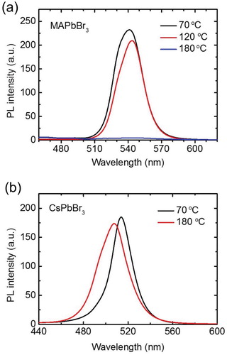
Figure 5. PL lifetime curves of the (a) MAPbBr3 and (b) CsPbBr3 polycrystalline films after annealing at 70°C, 120°C, or 180°C for 10 min.
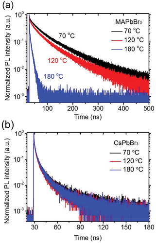
Table 4. Short PL lifetime ( ), long PL lifetime (), and average lifetime () of the MAPbBr3 and CsPbBr3 polycrystalline films depending on TANN ( is a statistical measure that evaluates the goodness of fit (the closer is to 1, the higher the fitting quality).
The decreases in the PL intensity and and the increase in the f1 of the MAPbBr3 films with increasing TANN can be clearly explained by the thermal decomposition of MAPbBr3, confirmed in the SEM images and XRD patterns (Figures and ); the destruction of the MHP crystal lattice generates numerous defects that act as trapping sites for charge carriers, and consequently causes trap-assisted non-radiative recombination, which in turn decreases the PL intensity and lifetime [Citation41]. In contrast to MAPbBr3, thermal decomposition did not occur in CsPbBr3 even at TANN = 230°C, and thereby, the radiative recombination process in CsPbBr3 was not much changed.
4. Conclusion
A comparative study was conducted to determine how the A-site cation affects the thermal stability of MHP polycrystalline films. An OIH MHP (MAPbBr3) and an AI MHP (CsPbBr3) were compared. The MAPbBr3 films were much less thermally stable than CsPbBr3 films; the MAPbBr3 films thermally decomposed into PbBr2 when annealed at TANN ≥ 180°C; the XRD pattern of the MAPbBr3 film annealed at 230°C matched the calculated pattern of PbBr2; i.e. the MAPbBr3 had completely decomposed. The steady-state PL intensity and PL lifetime of the MAPbBr3 films decreased significantly as TANN increased because the thermal decomposition of MAPbBr3 increases the trap-assisted non-radiative recombination. In contrast, the CsPbBr3 films were not significantly degraded by annealing even at 230°C; the film morphology and XRD patterns were maintained. The steady-state PL intensity and PL lifetime of the CsPbBr3 films were only slightly decreased by annealing at 180°C. These results can provide a way of overcoming the thermal instability of MHPs for application to optoelectronics.
Disclosure statement
No potential conflict of interest was reported by the authors.
Additional information
Funding
Notes on contributors

Himchan Cho
Himchan Cho received his B.S. (2012.02) and Ph.D. (2016.08) Materials Science and Engineering degrees from Pohang University of Science and Technology (POSTECH), Republic of Korea. He is currently working as a postdoctoral researcher in the Materials Science and Engineering Department, BK21 PLUS SNU Materials Division for Educating Creative Global Leaders of Seoul National University, South Korea (2016.09-present). His research interests include metal halide perovskites and their application to optoelectronics.

Joo Sung Kim
Joo Sung Kim received his B.S. Materials Science and Engineering degree from Pohang University of Science and Technology (POSTECH) in 2016. He is currently pursuing a Ph.D. degree in materials science and engineering at Seoul National University (integrated course). His research interests include organic–inorganic hybrid optoelectronics, organic light-emitting diodes, and spectroscopy.

Young-Hoon Kim
Young-Hoon Kim received his M.S. (2014) Environmental Science and Engineering and Ph.D. (2016) Material Science and Engineering degrees from Pohang University of Science and Technology (POSTECH), South Korea. He is currently working in the Materials Science and Engineering Department of Seoul National University, South Korea as a postdoctoral researcher (2016–2017). His research focuses on solution-processed electronics based on organic and organic–inorganic hybrid materials for flexible displays and solid-state lighting.

Tae-Woo Lee
Tae-Woo Lee is an associate professor in the Materials Science and Engineering Department of Seoul National University, South Korea. He received his Ph.D. degree in chemical engineering from KAIST, South Korea in 2002. He joined Bell Laboratories, USA as a postdoctoral researcher, and worked at Samsung Advanced Institute of Technology as a research staff member (2003–2008). He was an associate professor in the Materials Science and Engineering Department of Pohang University of Science and Technology (POSTECH), South Korea until August 2016. His research focuses on printed electronics based on organic and organic–inorganic hybrid materials for flexible displays, solid-state lighting, and solar-energy-conversion devices.
References
- Y.-H. Kim, H. Cho, and T.-W. Lee, Proc. Natl. Acad. Sci. U. S. A. 113, 11694–11702 (2016). doi: 10.1073/pnas.1607471113
- Y.-H. Kim, C. Wolf, Y.-T. Kim, H. Cho, W. Kwon, S. Do, A. Sadhanala, C.G. Park, S.-W. Rhee, S.H. Im, R.H. Friend, and T.-W. Lee, ACS Nano 11, 6586–6593 (2017). doi: 10.1021/acsnano.6b07617
- Y.-H. Kim, G.-H. Lee, Y.-T. Kim, C. Wolf, H.J. Yun, W. Kwon, C.G. Park, and T.-W. Lee, Nano Energy 38, 51–58 (2017). doi: 10.1016/j.nanoen.2017.05.002
- J. Pan, L.N. Quan, Y. Zhao, W. Peng, B. Murali, S.P. Sarmah, M. Yuan, L. Sinatra, N.M. Alyami, J. Liu, E. Yassitepe, Z. Yang, O. Voznyy, R. Comin, M.N. Hedhili, O.F. Mohammed, Z.H. Lu, D.H. Kim, E.H. Sargent, and O.M. Bakr, Adv. Mater. 28, 8718–8725 (2016). doi: 10.1002/adma.201600784
- L. Protesescu, S. Yakunin, M.I. Bodnarchuk, F. Krieg, R. Caputo, C.H. Hendon, R.X. Yang, A. Walsh, and M. V. Kovalenko, Nano Lett. 15, 3692–3696 (2015). doi: 10.1021/nl5048779
- H. Cho, C. Wolf, J.S. Kim, H.J. Yun, J.S. Bae, H. Kim, J.-M. Heo, S. Ahn, and T.-W. Lee, Adv. Mater. 29, 1700579 (2017). doi: 10.1002/adma.201700579
- C. Wolf, J.-S. Kim, and T.-W. Lee, ACS Appl. Mater. Interfaces 9, 10344–10348 (2017). doi: 10.1021/acsami.6b15694
- A. Sadhanala, F. Deschler, T.H. Thomas, S.E. Dutton, K.C. Goedel, F.C. Hanusch, M.L. Lai, U. Steiner, T. Bein, P. Docampo, D. Cahen, and R.H. Friend, J. Phys. Chem. Lett. 5, 2501–2505 (2014). doi: 10.1021/jz501332v
- H. Cho, S.-H. Jeong, M.-H. Park, Y.-H. Kim, C. Wolf, C.-L. Lee, J.H. Heo, A. Sadhanala, N. Myoung, S. Yoo, S.H. Im, R.H. Friend, and T.-W. Lee, Science 350, 1222–1225 (2015). doi: 10.1126/science.aad1818
- Y.-H. Kim, H. Cho, J.H. Heo, T.-S. Kim, N. Myoung, C.-L. Lee, S.H. Im, and T.-W. Lee, Adv. Mater. 27, 1248–1254 (2015). doi: 10.1002/adma.201403751
- Z.-K. Tan, R.S. Moghaddam, M.L. Lai, P. Docampo, R. Higler, F. Deschler, M. Price, A. Sadhanala, L.M. Pazos, D. Credgington, F. Hanusch, T. Bein, H.J. Snaith, and R.H. Friend, Nat. Nanotechnol. 9, 687–692 (2014). doi: 10.1038/nnano.2014.149
- Z. Xiao, R.A. Kerner, L. Zhao, N.L. Tran, K.M. Lee, T.-W. Koh, G.D. Scholes, and B.P. Rand, Nat. Photonics 11, 108–115 (2017). doi: 10.1038/nphoton.2016.269
- M. Yuan, L.N. Quan, R. Comin, G. Walters, R. Sabatini, O. Voznyy, S. Hoogland, Y. Zhao, E.M. Beauregard, P. Kanjanaboos, Z. Lu, D.H. Kim, and E.H. Sargent, Nat. Nanotechnol. 11, 872–877 (2016). doi: 10.1038/nnano.2016.110
- N. Wang, L. Cheng, R. Ge, S. Zhang, Y. Miao, W. Zou, C. Yi, Y. Sun, Y. Cao, R. Yang, Y. Wei, Q. Guo, Y. Ke, M. Yu, Y. Jin, Y. Liu, Q. Ding, D. Di, L. Yang, G. Xing, H. Tian, C. Jin, F. Gao, R.H. Friend, J. Wang, and W. Huang, Nat. Photonics 10, 699–704 (2016). doi: 10.1038/nphoton.2016.185
- J. Byun, H. Cho, C. Wolf, M. Jang, A. Sadhanala, R.H. Friend, H. Yang, and T.-W. Lee, Adv. Mater. 28, 7515–7520 (2016). doi: 10.1002/adma.201601369
- S.-H. Jeong, S.-H. Woo, T.-H. Han, M.-H. Park, H. Cho, Y.-H. Kim, H. Cho, H. Kim, S. Yoo, and T.-W. Lee, NPG Asia Mater. 9, e411 (2017). doi: 10.1038/am.2017.108
- L. Zhang, X. Yang, Q. Jiang, P. Wang, Z. Yin, X. Zhang, H. Tan, Y.M. Yang, M. Wei, B.R. Sutherland, E.H. Sargent, and J. You, Nat. Commun. 8, 15640 (2017). doi: 10.1038/ncomms15640
- G. Xing, N. Mathews, S.S. Lim, N. Yantara, X. Liu, D. Sabba, M. Grätzel, S. Mhaisalkar, and T.C. Sum, Nat. Mater. 13, 476–480 (2014). doi: 10.1038/nmat3911
- F. Deschler, M. Price, S. Pathak, L.E. Klintberg, D.D. Jarausch, R. Higler, S. Hüttner, T. Leijtens, S.D. Stranks, H.J. Snaith, M. Atatüre, R.T. Phillips, and R.H. Friend, J. Phys. Chem. Lett. 5, 1421–1426 (2014). doi: 10.1021/jz5005285
- H. Yuan, E. Debroye, G. Caliandro, K.P.F. Janssen, J. van Loon, C.E.A. Kirschhock, J.A. Martens, J. Hofkens, and M.B.J. Roeffaers, ACS Omega 1, 148–159 (2016). doi: 10.1021/acsomega.6b00107
- S. Lee, J.H. Park, B.R. Lee, E.D. Jung, J.C. Yu, D. Di Nuzzo, R.H. Friend, and M.H. Song, J. Phys. Chem. Lett. 8, 1784–1792 (2017). doi: 10.1021/acs.jpclett.7b00372
- Y.-H. Kim, H. Cho, J.H. Heo, S.H. Im, and T.-W. Lee, Curr. Appl. Phys. 16, 1069–1074 (2016). doi: 10.1016/j.cap.2016.06.002
- A. Pisoni, J. Jaćimović, O.S. Barišić, M. Spina, R. Gaál, L. Forró, and E. Horváth, J. Phys. Chem. Lett. 5, 2488–2492 (2014). doi: 10.1021/jz5012109
- M. Kulbak, S. Gupta, N. Kedem, I. Levine, T. Bendikov, G. Hodes, and D. Cahen, J. Phys. Chem. Lett. 7, 167–172 (2016). doi: 10.1021/acs.jpclett.5b02597
- B. Conings, J. Drijkoningen, N. Gauquelin, A. Babayigit, J. D’Haen, L. D’Olieslaeger, A. Ethirajan, J. Verbeeck, J. Manca, E. Mosconi, F. De Angelis, and H.-G. Boyen, Adv. Energy Mater. 5, 1500477 (2015). doi: 10.1002/aenm.201500477
- A. Latini, G. Gigli, and A. Ciccioli, Sustain. Energy Fuels 1, 1351–1357 (2017). doi: 10.1039/C7SE00114B
- W. Zhu, C. Bao, Y. Wang, F. Li, X. Zhou, J. Yang, B. Lv, X. Wang, T. Yu, and Z. Zou, Dalt. Trans. 45, 7856–7865 (2016). doi: 10.1039/C6DT00900J
- B. Roose, A. Ummadisingu, J.-P. Correa-Baena, M. Saliba, A. Hagfeldt, M. Graetzel, U. Steiner, and A. Abate, Nano Energy 39, 24–29 (2017). doi: 10.1016/j.nanoen.2017.06.037
- E. Tenuta, C. Zheng, and O. Rubel, Sci. Rep. 6, 37654 (2016). doi: 10.1038/srep37654
- M. Lumbreras, J. Protas, S. Jebbari, G.J. Dirksen, and J. Schoonman, Solid State Ionics 20, 295–304 (1986). doi: 10.1016/0167-2738(86)90049-4
- A. Dualeh, N. Tétreault, T. Moehl, P. Gao, M.K. Nazeeruddin, and M. Grätzel, Adv. Funct. Mater. 24, 3250–3258 (2014). doi: 10.1002/adfm.201304022
- T. Supasai, N. Rujisamphan, K. Ullrich, A. Chemseddine, and T. Dittrich, Appl. Phys. Lett. 103, 183906 (2013). doi: 10.1063/1.4826116
- N. Yantara, S. Bhaumik, F. Yan, D. Sabba, H.A. Dewi, N. Mathews, P.P. Boix, H.V. Demir, and S. Mhaisalkar, J. Phys. Chem. Lett. 6, 4360–4364 (2015). doi: 10.1021/acs.jpclett.5b02011
- C.C. Stoumpos, C.D. Malliakas, J.A. Peters, Z. Liu, M. Sebastian, J. Im, T.C. Chasapis, A.C. Wibowo, D.Y. Chung, A.J. Freeman, B.W. Wessels, and M.G. Kanatzidis, Cryst. Growth Des. 13, 2722–2727 (2013). doi: 10.1021/cg400645t
- J. Zhao, Y. Deng, H. Wei, X. Zheng, Z. Yu, Y. Shao, J.E. Shield, and J. Huang, Sci. Adv. 3, eaao5616 (2017). doi: 10.1126/sciadv.aao5616
- S.R. Raga, M.-C. Jung, M. V. Lee, M.R. Leyden, Y. Kato, and Y. Qi, Chem. Mater. 27, 1597–1603 (2015). doi: 10.1021/cm5041997
- J.R. Lakowicz, Principles of Fluorescence Spectroscopy (Springer Science & Business Media, New York, NY, 2006).
- M. Vrućinić, C. Matthiesen, A. Sadhanala, G. Divitini, S. Cacovich, S.E. Dutton, C. Ducati, M. Atatüre, H. Snaith, R.H. Friend, H. Sirringhaus, and F. Deschler, Adv. Sci. 2, 1500136 (2015). doi: 10.1002/advs.201500136
- D. Shi, V. Adinolfi, R. Comin, M. Yuan, E. Alarousu, A. Buin, Y. Chen, S. Hoogland, A. Rothenberger, K. Katsiev, Y. Losovyj, X. Zhang, P.A. Dowben, O.F. Mohammed, E.H. Sargent, and O.M. Bakr, Science 347, 519–522 (2015). doi: 10.1126/science.aaa2725
- Q. Han, W. Wu, W. Liu, and Y. Yang, RSC Adv. 7, 35757–35764 (2017). doi: 10.1039/C7RA06211G
- A. Al Mamun, T.T. Ava, H.R. Byun, H.J. Jeong, M.S. Jeong, L. Nguyen, C. Gausin, and G. Namkoong, Phys. Chem. Chem. Phys. 19, 19487–19495 (2017). doi: 10.1039/C7CP03106H