
Abstract
In this paper, the effects of the combination of solvents on the uniformity of a dried emitting layer and on device performance were studied. Green emitter inks with various solvents were prepared, and it was seen that good film uniformity of printed layers could be obtained with a solvent mixture with different boiling points, which reduced the coffee ring effect on a dried surface. During the inkjet process, the drop injection condition aiming was also controlled for better drop-to-drop spacing and reduction of the line-edge roughness. Printed patterns of a small molecular/polymer hybrid emitting layer, composed of the chlorobenzene-dichlorobenzene solvent mixture, showed significantly reduced roughness of the microscopic surface and improved efficiency of the inkjet device, at levels nearly comparable to those of spin-coated patterns. A suitable hole transport layer (HTL) was also further developed as an interfacial material, prior to the solution processing of the emitter. The cross-linkable HTL was composed of triphenylamine as the cross-linking unit and a fluorene-based compound. At the optimized condition of the solvent formulation, printed droplets within 100 µm× 300 µm pixels formed a uniform stripe without remarkable coffee-ring defects and line-edge surface roughness.
1. Introduction
A printing process can be used for various low-cost organic electronic device applications such as organic thin film transistors, memory devices, organic solar cells, radio frequency identification (RFID) tags, and sensors. Although organic light-emitting diode (OLED) displays are widely used in the current mobile display market and in large-area TV sets with up to 8 k resolution (7680 × 4320 pixels), a more material- and cost-efficient alternative to vacuum thermal deposition with RGB side-by-side patterning is required for large-area OLED fabrication. Therefore, the printing-based OLED RGB pixel pattern technology has been developed in many groups and industries. The inkjet printing technique for micro-scale patterning is especially attracting the OLED industry because of its simple and large-area process capability [Citation1]. Advantages such as precision patterning quality, good material usage efficiency, and scalability make inkjet printing an ideal process for large-area OLED fabrication, while the supply of good soluble organic materials (inks) and proper handling of interfacial phenomena are still very important for the successful application of inkjet printing to OLED production. To obtain a high RGB pixel pattern quality, factors for satisfactory film formation, such as the ink formulation, viscosity, surface energy control, bank structure, and drying condition, are especially important. Furthermore, the pattern resolution can be enhanced by selective surface treatment, such as control of the hydrophilic/hydrophobic nature of pixel-defined structures (banks) [Citation2,Citation3].
Multiple attempts have been made to achieve successful inkjet printing of OLEDs in order to produce high pixel uniformity in large devices [Citation4–6] and effective printable materials [Citation7–10]. Recently, the intrinsic performance of solution-processed inkjet-printable materials has dramatically improved, almost reaching the level at which the inkjet process can already be considered for mass printing.
Although the inkjet process has many advantages, it still shows microscopic non-uniformity of the printed pixels. This phenomenon can be restricted, however, by controlling the baking temperature condition and the surface tension on the substrate and inks using the solvent formulation technology [Citation11]. Recently, a commercial large-area inkjet printer with a substrate particle contamination suppressing system was developed for the OLED ink system using a complicated solvent mixture, which is equipped with a nitrogen environment and fast in-flight inkjet droplet monitoring to provide highly accurate in-situ measurements for each nozzle.
In this study, the effect of a solvent mixture on the jetting and printing pixel uniformity of a stripe-type light emitting pattern was investigated. A mixture of solvents for phosphorescent green-emitting host materials was selected using a simple test of solubility, surface tension, and the boiling point window, and the chlorobenzene and 1,2-dichlorobenzene mixture was selected for better solubility of the methyl-substituted iridium complex dopant. The jetting of inks was investigated, and the surface uniformity after the drying process was observed. The device performance indicators of inkjet-printed samples with an optimum mixed solvent were compared, and they showed an efficiency as high as 90% of that of spin-coated references. The selection of the proper HTL (ink receptor surface) was important, not only for layer-by-layer stability, but also to maintain good pattern formation. This system employed dehydration condensation as a cross-linking reaction that can have a fast reaction time with the use of acid, and it formed novel cross-linkable HTLs composed of triphenylamine as the cross-linking unit and fluorene compounds as the basic unit. The corresponding improvement in the efficiency of the inkjet-printed device was illustrated.
2. Experiment section
2.1. Preparation of substrate pixels
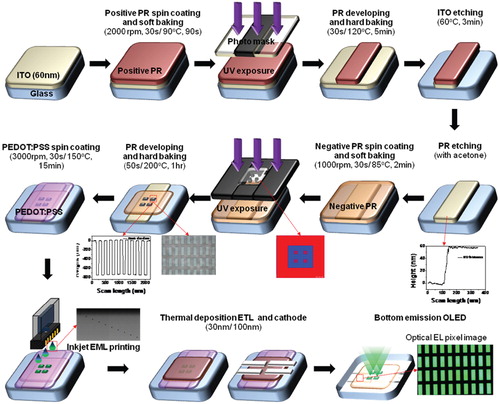
Stripe-patterned pixels were formed on an indium tin oxide (ITO) substrate. The cleaning processes were ultra-sonication in acetone and isopropanol at a 1:1 v/v ratio, boiling in a refreshed isopropanol solvent at 250°C, and baking in a vacuum chamber at 180°C for 30 min. The precise stripe-pixels were defined by a bank formed with a positive photoresist material (OrmoComp, purchased from Microresist Co., Ltd.) and a mask aligner (MDA-400S, Midas System, Korea) exposed to UV for 15 s. After post-exposure baking, developing, and final cleaning, the bank resist was hard-baked at 200°C. Figure is a schematic illustration of the process of ITO/bank photoresist patterning and inkjet printing for sample OLED devices. The pixel pattern defined by the photoresist bank (insulator) is rectangular in shape and 100 um wide, 300 um long, and 800 nm deep.
Figure 1. Schematic diagram of the overall process: stripe-patterned ITO test of the coupon cell, spin-coating of the hole injection layer, inkjet printing of the emitter, and evaporation for printed OLED fabrication.
2.2. Ink formulations
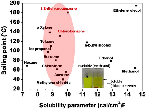
The selected host materials were composed of a small molecular material, 2,6-bis(3-(carbazol-9-yl)pyridine) [26DCzPPy], and a polymeric binder, poly(9-vinylcarbazole) [PVK, Mn:25,000]. Tris[2-(p-tolyl)pyridine]iridium(III) [Ir(mppy)3] was used as the phosphorescence green dopant material. We investigated several solvents (i.e. p-xylene, toluene, chlorobenzene, 1,2-dichlorobenzene, methanol, methylenechloride, isopropanol, and anisole) to find suitable candidates for EML inks. The investigated solvents have different boiling points and Hansen solubility parameters, shown in Figure . To formulate the green emitting inks, the host (26DCzPPy:PVK 1:1) and the dopant were first separately dissolved to have a 10% weight percentage in each solvent. Then each host-dopant solution was mixed at 10:1 (10% dopant concentration). The solubilizing effects of each solvent, and its appropriate condition as OLED ink, were characterized.
Figure 2. (a) Boiling temperature-solubility parameter graph with various organic solvents for the inkjet printing process, with photographs of organic emitting ink with typical good and poor solvents.
2.3. Device fabrication and measurement
Spin-coated PEDOT:PSS (AI4083, CleviosTM, Heraeus, Germany) was used as a hole injection layer (HIL) on top of the patterned ITO pixel, baked at 150°C for 10 min at 3,000 rpm per 30 s. HTL layers, whose synthetic process and optoelectronic data had been reported elsewhere, were spin-coated from the toluene onto the top of the PEDOT:PSS and annealed using a hot plate at 100°C for 30 min to remove the residual solvent. Non-crosslinkable TAPC {4,4′-Cyclohexylidenebis[N,N-bis(4-methylphenyl)benzenamine]} and BPBFTPA {4,4′-[1,10-biphenyl-4,4′-diylbis(9H-fluorene-9,9-diyl)] bis(N,N-di-p-tolylaniline)} were used as HTLs, with the latter capable of providing a cross-linked organic layer [Citation12].
After the PEDOT:PSS or PEDOT:PSS/HTL layer was heated, a mixture of hosts (26DCzPPy:PVK dissolved in the selected good solvent, chlorobenzene and 1,2-dichlorobenzene) were printed by supplying 1.5 mL ink to the piezoelectric nozzle (Dimatix, DMC-11610, Fujifilm, U.S.A.). The typical conditions are a proper waveform, a printing speed of 1 mm/s with a 3% meniscus (0.12 mPa), a working distance of 700 µm, and a stage temperature of 30°C. After the green ink droplet was printed in the bank-defined pixel covered with PEDOT:PSS/HTLs, EML was baked at 100°C for two hours in an N2 atmosphere. As in the reference samples, OLEDs with identical solvent compositions at EML were fabricated via spin-coating at 4,000 rpm for 30 s at the same baking condition. Both the spin-coated and inkjet-printed samples with a top EML were subjected to vacuum deposition, and bis(8-hydroxy-2-methylquinoline)-(4-phenlyphenoxy) aluminum and [BAlq, 5 nm]/tris-(8-hydroxyquinoline) aluminum [Alq3, 20 nm] were the hole blocking and electron transfer layer (ETL), respectively. Finally, lithium fluoride (LiF) (0.5 nm) and Al (100 nm) were deposited as the cathode layer. The current density–voltage-luminance characteristics of OLED devices were analyzed using the I-V-L measurement system (PR-655, Photo Research Co., U.S.A.) and Keithley 2400. All the purchased materials were used without further purification.
3. Results and discussion
Figure shows the boiling points and Hansen solubility parameter of each solvent tested in this study. It was observed that solvents with a solubility parameter in the range of 8–10(cal/cm3)F solubilized the 26DCzPPy, PVK, and Ir(mppy)3 completely irrespective of their boiling point (red circle in Figure ). However, polar molecules such as methanol, ethanol, and ethylene glycol, whose solubility parameters were in the range of 11–15(cal/cm3)F, were not effective. Considering the stability of ink (less tendency to evaporate during the jetting process), solvents with relatively high boiling points [chlorobenzene (CB), 1,2-dichlorobenzene (o-DCB), and p-xylene] were selected. Finally, a binary solvent with CB and o-DCB was chosen (due to its better performance in the droplet formation and jetting stability test; see Figure (a)), which represents an ideal jetting behavior with proper break-off phenomena and a suitable consolidation gap for each drop (about 500 µm). These two solvents significantly differ in their boiling points (CB: 132°C vs. o-DCB: 180°C) and surface tensions (CB: 33 mN/m vs. o-DCB: 37 mN/m). Therefore, if this solvent mixture is used as the ink of the organic EML layer, common defects of ink droplets after drying (induced by the coffee stain [Citation13] and tears of wine effect) might be supressed [Citation14,Citation15]. Meanwhile, the drop formation and jetting behavior of EML [26DCzPPy:PVK 1:1, containing 10 wt% Ir(mppy)3] in CB/o-DCB ink is shown in Figure (b–d). Unlike in the solute-free system (Figure (a)), the shape of the drops shows long tails (viscous drag) and distortion, which suggest jetting instability (Figure (b)). Such phenomenon can be improved by modifying the pulse voltage waveform to form a piezoelectric signal, as seen in Figure (c and d). Generally, the optimization of the timescale (trise, tdwell, and tfall) for a single polar waveform by determining the periodic variation can be attuned to the droplet velocity, droplet size, or meniscus motion to yield a stabilized jetting continuity [Citation16,Citation17]. Our optimized waveform condition was the result of the application of 25 V with a 2µs trise, 4µs tdwell, and 2µs tfall, which are the conditions for producing suitable pixel droplets for the fabrication of a thin emitting pixel pattern film with good uniformity. To reduce the line-edge roughness, the increase in the drop jetting frequency from 70 Hz to 200 Hz drop jetting and the more compact overlapping position (drop to drop distance) were helpful, as seen in Figure (e), with a typical printed line behavior at different drop spacing/delay conditions [Citation18]. The change from printed isolated drops to scalloped or more uniform lines from multiple drops can be seen.
Figure 3. (a) Drop formation and jetting behavior of the CB-oDCB solvents, showing a proper break-off phenomena and consolidation gap for each drop. (b) Pulse voltage waveform for forming a piezoelectric signal and an image of drop formation-jetting (25 V applied with 4µs tdwell without a rise/fall time). (c) 25 V applied with 1µs trise, 4µs tdwell, and 1µs tfall. (d) 25 V applied with 2µs trise, 4µs tdwell, and 2µs tfall. (e) Printed line behavior at different drop spacing/delay conditions – the change from printed isolated drops to scalloped or more uniform lines from multiple drops.
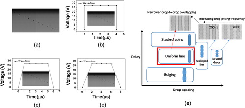
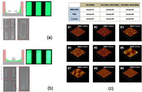
Figure shows the optical electroluminescence images and AFM surface morphology of the green emitter pixels printed by inkjet, with a size of 100 µm × 300 µm. In the case of printing with a single solvent (CB), the difference in the macroscopic thickness between the edge and the center area can be easily observed after drying, as seen in Figure (a). Moreover, the ink could not be filled uniformly inside the pixel defined by the bank structure, probably due to the mismatch of the surface tensions of CB and the OrmoComp resist (more hydrophilic). The low thickness at the pixel center seems to be a result of the coffee-ring effect and the over-spilling of the ink. These phenomena can be restricted with the use of solvent mixtures (CB:o-DCB, Figure (b)). Generally, mixing the host (26DCzPPy) with a polymeric compound (PVK) improves the surface roughness, showing a lower RMS (root mean square) value (Figure (c)). Adding o-DCB slightly alters the morphology of 26DCzPPy, but significantly reduces the RMS roughness of the host mixture with PVK, yielding only a 0.16–0.25 RMS roughness for 26DCzPPy:PVK:Ir(mppy)3/CB-oDCB 7:3 and 5:5, respectively.
Figure 4. (a) Schematic illustrations of the film formation after drying, image of the printed pixels, and the light-emitting photograph; (b) CB 100% solvents; and (c) CB-oDCB 5:5. (d) AFM roughness image and RMS values of 26DCzPPy, 26DCzPPy:PVK, and 26DCzPPy:PVK:Ir(mppy)3 upon printing with CB 100%, CB-oDCB 7:3, and CB-oDCB 5:5, respectively.
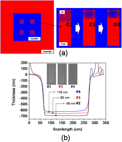
Further investigation of the in-pixel thickness profile of the inkjet-printed green emitter with the mixed solvent revealed a uniform layer formation. Figure (a) shows the layout for DPI (dot per inch) duplication adjustment in the designed pixel printing. Two-drop-column printing does not involve drop position duplication, but 3- and 4-drop-column duplication with the same droplet size corresponds to a higher DPI. As seen in the surface profilometer data in Figure (b), such an increase in DPI duplication without a change in the drop size resulted in the formation of a thicker film, with the thickness roughly proportional to the degree of the drop duplication. Although the ink with a single solvent could not uniformly fill the 100µm-width-scale bank pixel, CB-oDCB-mixed solvent ink could effectively fill the bank pixel, with a thickness controllable by the DPI duplication condition (Figure (b)).
Figure 5. (a) Control of the in-pixel thickness profile by DPI duplication without changing the drop size. (b) Surface profilometer data for the printed green emitter with the CB-oDCB 5:5 mixture solvent, showing the thickness of 46–110 nm by increasing the DPI duplication.
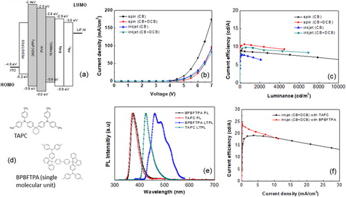
Finally, the green phosphorescence OLED was compared with the spin and inkjet-printed emitter. Figure (a) illustrates the device structure with the energy level diagram of each component of layers (the grayscale area is the emitter, the mixed compounds). In the case of these spin and printed devices with only a PEDOT:PSS hole injection layer, the current density behavior is shown in Figure (b). A higher current injection of the spin-coated device and the corresponding highest brightness with the CB single solvent were clearly observed, whereas the CB-oDCB (spin device) showed higher efficiency, probably due to the different thickness condition of the emitting layers for balanced device charge. For the inkjet devices, this CB-oDCB mixture yielded a more stable IVL curve and higher efficiency, maintained at around 10 cd/A at the range of luminance of up to 2,000 cd/m2. The non-uniformity of the inkjet-printed device with the CB single solvent (Figure (a)) could have reduced the cd/A efficiency and the brightness, as shown in Figure (c). The insertion of the organic soluble HTL between PEDOT:PSS and the solution-processed emitting layer and the cross-linking of the HTL materials were found to be effective in drastically improving the chemical and interfacial stability of solution-processed multilayers, both for OLED and Quantum Dot LEDs [Citation19–21]. The properties of solution-processable small molecular thin films that can be transformed into an insoluble layer by an amine-alcohol condensation reaction have been previously reported, and the detailed procedure has been illustrated elsewhere [Citation20,Citation21]. Figure (d) shows the materials for the HTL interface layer materials TAPC and BPBFTPA. In the case of the BPBFTPA cross-linking, a dehydration condensation reaction occurs with the heat treatment of the low-molecular-weight materials biphenyl-bis(fluorenol) and triphenylamine in the presence of an acetic acid/trifluoroacetic acid mixture, wherein the intactness of BPBFTPA under the attack of solvents was tested by comparing it with the UV-Vis absorption intensity [Citation12]. Figure (e) shows the room temperature solution photoluminescence and low temperature photoluminescence properties of TAPC and BPBFTPA, particularly their high triplet state energies (T1), which make them suitable for green and blue OLED HTLs. The inkjet device properties with TAPC and BPBFTPA interfacial HTL layers are shown in Figure (f). The maximum current efficiency reached 25 cd/A, comparable to that in reports of the best inkjet-printed devices with green Ir complex emitters (23.8 cd/A and an EQE of 7.2% [Citation22]; 28.2 cd/A and an EQE of 8.9% [Citation15]; etc.). Even though the TAPC layer may not survive after the layer-by-layer printing process, its infinitesimal residue at the interface plays a role in the improvement of the device efficiency. The device efficiency could be further improved with the use of BPBFTPA cross-linkable HTL units, but in this study, the efficiency improvement was confined to the low current density region. To further improve the hole transport ability and performance of devices with cross-linked HTLs, a cross-linked layer must be formed and the thickness of the BPBFTPA unit must be controlled by optimizing the amine-alcohol condensation reaction.
Figure 6. (a) Device structure and energy level diagram (for each layer) of the soluble/printed OLED with an emitter on HIL (PEDOT:PSS). (b) Current density vs. voltage. (c) Luminance vs. current density. (d) Chemical structure of the HTL interface materials (TAPC and BPBFTPA). (e) Room and low-temperature PL of the HTLs. (f) Current density vs. efficiency of the printed OLED with the emitter on HTLs.
4. Conclusion
In this study, the inkjet-printed pixel pattern quality of OLED with solvent mixture-based emitter ink was investigated. After the printed pixels were dried, the ink with the CB-oDCB mixture formed a more uniform microscopic surface and homogeneous filling of the bank structure via suitable DPI jetting position duplication, which, when controlled, yielded a 46–110 nm-thick film. The formulation of the solvent mixture by adding high-boiling-point oDCB was found to be effective in improving the pattern quality of a dried film of the 26DCzPPy:PVK:Ir(mppy)3 solution via inkjet printing. Although the current efficiency of a 10cd/A inkjet-printed device is slightly lower than that of the spin-coated reference, the inkjet device showed an efficiency of almost 90% of that of the spin-coated device. A suitable hole transport layer, as an interfacial material prior to the solution processing of the emitter, was used to further improve the properties of the inkjet device. The cross-linkable HTL composed of triphenylamine and a fluorene-based unit contributed to the high efficiency of the device with higher than 20cd/A efficiency, but its limited current injection might have been responsible for the low brightness properties.
Acknowledgments
This research was supported by the industrial strategic technology development program (20011059, Development of inks for emitting layers with high performance and long lifetime for printing process) funded by the Ministry of Trade, Industry & Energy; MOTIE, Korea).
Disclosure statement
No potential conflict of interest was reported by the author(s).
Additional information
Funding
Notes on contributors

Dai Geon Yoon
Dai Geon Yoon received his B.S., M.S., and Ph.D. degrees in Polymer Science and Engineering from Dankook University in Yongin, Korea in 2010, 2012, and 2016, respectively. After graduating, he worked as a postdoctoral researcher at the Korea Institute of Industrial Technology in 2018. He is currently a senior researcher at SEMES Corporation. His research interests are the manufacturing process, equipment design for quantum dot/OLED display devices, and rheological analysis of inks.

You Jung Kang
You-Jung Kang received her B.S. and M.S. degrees in Polymer Science and Engineering from Dankook University in Yongin, Korea in 2018 and 2020, respectively. Her research area is the development of ink formulation and printed patterns for patterned OLED devices using inkjet printing processes.

Robert Bail
Robert Bail joined Dankook University, Korea as a lecturer in 2014 after completing both his M.S. and Ph.D. degrees at the University of Nottingham in Nottingham, United Kingdom in 2009 and 2013, respectively. Since then, he has been in-charge of teaching more than 400 engineering students yearly how to develop, model, and prototype their own product ideas. Robert’s research interests are 3D printing, inkjet printing, and solution processing of polymers, small molecular materials, and quantum-dot materials for display and other emerging applications. He has also been a co-investigator in the group of Prof. Byung Doo Chin since 2015.

Byung Doo Chin
Byung Doo Chin received his B.S. degree from Yonsei University in Seoul, Korea and his M.S. and Ph.D. degrees in Chemical Engineering from the Korea Advanced Institute of Science and Technology in Daejeon, Korea in 1994, 1996, and 2000, respectively. After graduating, he worked as a postdoctoral scientist at the University of Massachusetts in Amherst, Massachusetts, U.S.A. and later, as a senior engineer at the Samsung SDI R&D Center and at the Korea Institute of Science and Technology. Since 2009, he has been working as a professor in the Polymer Science and Engineering Department of Dankook University in Yongin, Korea. His researches for about 20 years are on the AMOLED front-plane device physics and fabrication process, quantum dot light-emitting devices patterned by inkjet/nozzle printing, and the light extraction structure for flexible OLEDs.
References
- C.-H. Oh, H.-J. Shin, W.-J. Nam, B.-C. Ahn, S.-Y. Cha, and S.-D. Yeo, SID Symp. Digest Tech. Pap. 44, 239 (2013).
- J.Z. Wang, Z.H. Zheng, H.W. Li, W.T.S. Huck, and H. Sirringhaus, Nat. Mater. 3, 171 (2004).
- R. Cobas, S. Munoz-Perez, S. Cadogan, M.C. Ridgway, and X. Obradors, Adv. Funct. Mater. 25, 765 (2014).
- C. Brown, “OLED degradation”, workshop presented at 18 August 2015, IMID, Taegu, Korea; C. Madigan, S.Van Slyke, E. Vronsky, “Inkjet printing equipment for organic LED mass production”, 17 July 2015, SPIE Newsroom. DOI:10.1117/2.1201506.005940
- P.-Y. Chen, C.-L. Chen, C.-C. Chen, L. Tsai, H.-C. Ting, L.-F. Lin, C.-C. Chen, C.-Y. Chen, L.-H. Chang, T.-H. Shih, Y.-H. Chen, J.-C. Huang, M.-Y. Lai, C.-M. Hsu, and Y. Lin, SID Symp. Digest Tech. Pap. 45, 396 (2014).
- C.F. Madigan, C.R. Hauf, L.D. Barkley, N. Harjee, E. Vronsky, and S.A. Van Slyke, SID Symp. Digest Tech. Pap. 45, 399 (2014).
- A. Hayer, R. Anémian, T. Eberle, S. Heun, A. Ludemann, N. Schulte, and H. Buchholz, J. Inf. Disp. 12, 57 (2011).
- I. Ogawa, PLEDs, Flexible Displays and Printed Electronics (OLEDs World Summit: Berkeley, CA, USA, 2014).
- K.S. Yook, and J.Y. Lee, Adv. Mater. (Weinheim, Ger.) 26, 4218 (2014).
- Y.-H. Kim, C. Wolf, H. Cho, S.-H. Jeong, and T.-W. Lee, Adv. Mater. (Weinheim, Ger.) 28, 734 (2016).
- Z. Ding, R. Xing, Q. Fu, D. Ma, and Y. Han, Org. Elect. 12, 703 (2011).
- B.S. Kim, O. Kim, B.D. Chin, C.W. Lee, and J. Kor, Phys. Soc. 72, 930 (2018).
- R.D. Deegan, O. Bakajin, T.F. Dupont, G. Huber, S.R. Nagel, and T.A. Witten, Nature 389, 827 (1997).
- C. Jiang, Z. Zhong, B. Liu, Z. He, J. Zou, L. Wang, J. Wang, J. Peng, and Y. Cao, ACS Appl. Mater. Interfaces 8, 26162 (2016).
- Y.J. Kang, R. Bail, C.W. Lee, and B.D. Chin, ACS Appl. Mater. Interfaces 11, 21784 (2919).
- H.Y. Gan, X.C. Shan, T. Eriksson, B.K. Lok, and Y.C. Lam, J. Micromech. Microeng. 19, 055010 (2009).
- P.H. Shin, S.J. Lee, J.Y. Sung, and J.H. Kim, Microelectron. Reliab. 51, 437 (2011).
- D. Soltman, and V. Subrmanian, Langmuir 24, 2224 (2008).
- C. Zuniga, S. Barlow, and S.R. Marder, Chem. Mater. 23, 658 (2011).
- S.J. Cha, S. Cho, W. Lee, H. Chung, I. Kang, and M.C. Suh, Macromol. Rapid Commun. 35, 807 (2014).
- L. Xie, X. Xiong, Q. Chang, X. Chen, C. Wei, X. Li, M. Zhang, W. Su, and Z. Cui, Small 15, 1900111 (2019).
- Y.-X. Hu, T. Lin, X. Xia, W.-Y. Mu, Y.-L. Sun, W.-Z. He, C.-T. Wei, D.-Y. Zhang, X. Li, and Z. Cui, J. Mater. Chem. C 7, 4178 (2019).