
Abstract
Organic light-emitting diode (OLED) microdisplays have attracted much attention as displays for small form factor augmented reality (AR) devices. To realize glass-like thin and wide field of view (FoV) AR devices, we designed a display module with a high aspect ratio microdisplay and a thin optical component. For the high aspect ratio microdisplay, we developed the color OLED microdisplay with a 32:9 aspect ratio and a 0.8-inch diagonal ∼2,490-ppi CMOS backplane. To express color and reduce optical crosstalk, we fabricated the color filter (C/F) patterning directly on the white OLED. We also developed a pin mirror lens with 11 pin mirrors to improve the optical efficiency and quality with a thin lens. By combining the microdisplay with LetinAR’s pin mirror lens, we successfully demonstrated an AR device with a wide horizontal FoV of 46° but with a small form factor 4 mm lens.
KEYWORDS:
1. Introduction
Demand is increasing for light, compact, and high-resolution displays for the implementation of augmented reality (AR) under a mobile environment. Microdisplays are small, lightweight, and high-resolution, which make them suitable for AR devices. Among microdisplays, organic light-emitting diode (OLED) microdisplays have attracted much attention because their self-emissive property can effectively reduce the form factor of AR devices [Citation1–3].
For small form factor AR devices, the OLED microdisplay should be combined with an optical system that has light, thin, and high optical characteristics. Optical systems that use diffractive/holographic waveguide optics are light and thin [Citation4], but their optical efficiency is very low, which make them inappropriate for combining with the OLED microdisplay. Recently, LetinAR developed an optical system based on a pin mirror lens [Citation5]. Using the pin mirror lens, an expandable eyebox and field of view (FoV), an extended depth of field, and high optical efficiency can be achieved with a lens as thick as a typical eyeglass lens. In addition, this optical system can be easily combined with the OLED microdisplay by putting the OLED microdisplay on top of the lens, thereby realizing a glass-like AR device. In this system, the thickness of the lens corresponds to the vertical size of the OLED microdisplay, so the aspect ratio of the microdisplay limits the horizontal FoV. In addition, since the interpupillary distance (IPD) differs from person to person, a wide screen display has the advantage of being able to adjust the screen to the wearer’s IPD without a mechanical slider for small form factor AR devices. Thus, by considering FoV and IPD, the OLED microdisplay with a high aspect ratio should be developed.
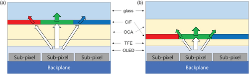
Developing a color OLED microdisplay is also important to expand its applications. White OLEDs with color filter (C/F) patterning are widely used in OLED microdisplays due to the ease of the high-resolution patterning [Citation6,Citation7]. Generally, as shown in Figure (a), the C/F is first patterned on a separate substrate and then attached to the OLED display panel using an optically clear adhesive (OCA) due to the high process temperature of C/F formation. The typical thickness of the OCA in an OLED display is more than tens of μm, longer than the sub-pixel size of microdisplays, resulting in optical crosstalk. As the adjacent sub-pixel has different colors, this optical crosstalk can decrease the color purity of the pixel. To reduce optical crosstalk, the distance between the C/F and the white OLED should be smaller than the size of the sub-pixels [Citation8].
Figure 1. Vertical structure of the OLED display with (a) the conventional color filter (C/F) patterning method and (b) C/F patterning directly on the OLED.
In this study, we designed a display module with a high aspect ratio microdisplay and a thin optical component. For the high aspect ratio microdisplay, we developed the color OLED microdisplay with a 32:9 aspect ratio. To express color and reduce optical crosstalk, we fabricated the C/F patterning directly on the OLED. Since the distance between the C/F and the white OLED was a few times smaller than the sub-pixel size, the optical crosstalk was effectively reduced. Thus, we successfully demonstrated a wide (46°)- horizontal FoV AR device by using a color OLED microdisplay integrated with LetinAR’s 4 mm pin mirror lens.
2. Experiments
Figure (b) shows the vertical structure of the OLED microdisplay. The backplane was designed by RAONTECH and fabricated on an 8-inch Si wafer via the 0.11μm CMOS process. The sub-pixel size was 3.4 μm × 10.2 μm, the diagonal display size was 0.8 inch, and the display resolution was 1,920 × 540, which resulted in ∼2,490 pixels per inch (ppi). To drive the logic circuits and OLED pixels, 1.8 and 7 V transistor processes were adopted [Citation9–12]. After the backplane was fabricated, it was successively cleaned with isopropyl alcohol and acetone, and dried in a vacuum oven at 120°C. Then the organic layers and the top metal were deposited by a thermal evaporator to fabricate the OLED. The structures of the OLEDs used in the experiments are summarized in Table . After the OLED fabrication, an Al2O3 and SiNx bi-layered passivation layer was deposited via atomic layer deposition (ALD) under 95°C and via plasma-enhanced chemical vapor deposition (PECVD) under 100°C. Next, the Al2O3/SiNx bi-layered passivation layer was dry-etched to open the contact pads. Then the C/Fs were patterned on the passivation layer using an i-line stepper. The C/Fs were supplied by Dongwoo Fine-Chem Co., Ltd. After the device was fabricated, the cover glasses were attached to the OLED microdisplays. Then the OLED microdisplays were mounted on printed circuit boards (PCBs) and connected through wire bonding. Finally, the OLED microdisplays were controlled by driving circuit boards and connected with a flat flexible cable (FFC).
Table 1. Structures of the OLEDs used in the experiments, where HIL, HTL, YG, ETL, HAT-CN, TCTA, BmPyPB, NPB, CGL, and B refer to the hole injection layer; hole transport layer; yellow-green emitting layer; electron transport layer; 1,4,5,8,9,11-hexaazatriphenylene hexacarbonitrile; 4,4′,4″-Tri(N-carbazolyl)triphenylamine; 1,3-bis(3,5-dipyrid-3-yl-phenyl)benzene; N,N′-bis(naphthalen-1-yl)-N,N′-bis(phenyl)benzidine; charge generation layer; and blue emitting layer, respectively.
The current density–voltage–luminance (J–V–L) characteristics of the OLED were measured using a source measurement unit (Keithley 238) and a spectroradiometer (Konica Minolta CS-2000). The transmittances of the C/Fs were measured with a UV/VIS/NIR spectrometer (PerkinElmer Lambda 750). The FoV was measured using the near eye display measurement system (Gamma Scientific NED-LMD E101), which is composed of a luminance-measuring camera and a goniometric robot arm. For the FoV measurement, the eye relief, which is the distance between the measuring camera and the pin mirror lens, was set at 15 mm, and the measuring camera was rotated vertically and horizontally on the axis at the entrance pupil of the camera. The cutoff angle was defined to the point at half-luminance.
3. Results and discussion
3.1. The low-temperature processes for direct C/F patterning on OLEDs
Since common organic semiconductors are vulnerable to high temperature [Citation13], a low process temperature is essential. To protect the OLED from the moisture, oxygen, and chemicals used in the subsequent process, low-temperature processed thin film encapsulation (TFE) is utilized. The low-temperature atomic layer deposition (ALD) of an Al2O3 layer exhibits an excellent gas barrier property that makes it appropriate to use as the TFE for OLEDs. To observe the device damage during the ALD process, the electro-optical characteristics of the OLEDs before and after ALD were compared. First, the single top-emitting yellow-green (YG) OLED structure with a total thickness of 270 nm, corresponding to the tandem structure, was used for the ALD damage test. As shown in Figure (a), before ALD, the current density and luminance at 6 V were 0.135 A/cm2 and 6,685 cd/m2, respectively, and after ALD, 0.146 A/cm2 and 5,553 cd/m2, respectively. The J–V–L characteristics of the OLEDs were not significantly degraded after the TFE process. Similarly, the TFE layer was successfully applied to the tandem device structure without damage.
Figure 2. (a) J–V–L characteristics of the single YG OLED before and after Al2O3 TFE. (b) J–V–L characteristics of the tandem OLED with the Al2O3/SiNx passivation layer according to the immersion time in the developer. The detailed structures are described in Table .
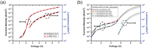
Even though the Al2O3 exhibited good gas permeation, the TFE should protect the OLED from the chemicals used in the subsequent patterning process. Unfortunately, the developer damaged the OLED in the photolithography process, possibly due to pinhole defects and contaminants in the laboratory-level environment. To protect the OLEDs from the chemicals, a chemically robust, optically transparent in the visible region, and low-temperature processible SiNx layer was selected as the second passivation layer. After the SiNx deposition, the OLED was not washed for 10 min under immersion in the developer. As shown in Figure (b), the current densities at 10 V after immersion in the developer for 0, 2, 6, and 10 min were 0.067, 0.062, 0.061, and 0.038 A/cm2, respectively. The device that used the bi-layered TFE (Al2O3/SiNx) showed stable J–V–L characteristics after immersion in the developer for 6 min. The development time for the C/F patterning was 1 min for each color, and the total development time, including the pad open process, was less than 4 min. Thus, the bi-layered TFE layer that tolerated the immersion test for 6 min was sufficient for use in the subsequent patterning processes. The increased current in the leakage region is possibly due to the thermal stress and the additional sample handling step during the immersion process [Citation14,Citation15].
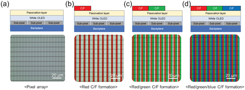
Later, the C/Fs were patterned on the TFE layer. The C/F process temperature is usually higher than 200°C, which makes it unsuitable for direct patterning on the OLED. To reduce the C/F process temperature, both C/F materials and low-temperature processes should be developed. In this study, we used UV irradiation as a photonic curing method to bring the C/F process temperature below 100°C. After the UV irradiation, the C/F pattern was not peeled off in the successive patterning steps. The stripe pattern was adopted for the C/F formation. The width of each C/F was designed as 3.6 μm, 200 nm larger than the sub-pixel pitch. Thus, the C/Fs overlapped by 200 nm, where the light was ideally completely absorbed by the different C/Fs. In addition, because the alignment error of the i-line stepper was less than 200 nm, the C/Fs were fully covered in the light-emitting area, otherwise, the white light would have leaked, which would have adversely affected the color purity. As shown in Figure (b–d), the red, green, and blue C/F patterns were well formed and did not peel off during the subsequent C/F processes. The distance between the OLED and C/F was around 1 μm, approximately 3 times shorter than sub-pixel size, resulting in reduced optical crosstalk. In addition, the refractive index of the SiNx is higher than organic semiconductors, the light with incident angle is refracted to the normal direction, beneficial for achieving low optical crosstalk.
Figure 3. Optical microscope images of the pixel array area (a) before and (b) after the C/F patterning with the vertical structures.
3.2. The high aspect ratio color OLED microdisplay
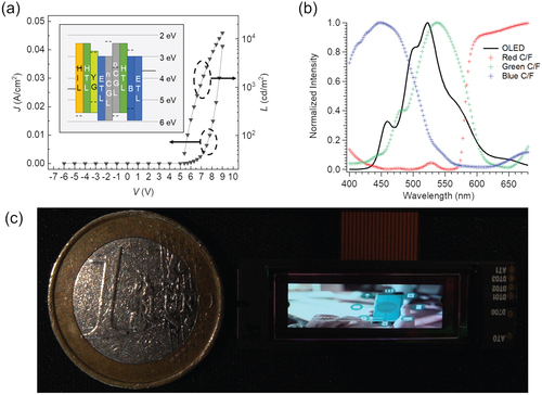
A two-wavelength white OLED with a tandem structure was used to improve efficiency and operational stability [Citation16]. The tandem OLED consisted of fluorescent blue and phosphorescent YG emitting layers, connected by the charge generation layer (CGL). To achieve high efficiency, the thickness and the location of the emitting layer were optically simulated. Due to the microcavity effect, the optimal cavity length differed according to the emission spectrum. From the efficiency viewpoint, the total thickness was determined up to the region between the maximized blue intensity point and the maximized YG intensity point, which was 210–280 nm. From the spectrum viewpoint, it was better to locate YG at the 1st cavity order and B at the 2nd cavity order to achieve a broad spectrum. Matching the cavity length to the green region helped produce both blue and red emissions. The electron–hole balance should also be considered. The mobility of the hole transport layer (HTL) is typically faster than that of the electron transport layer (ETL), which indicates that the HTL should be thicker than the ETL for a good charge balance. By considering the aforementioned design rules, the total thickness, the 1st HTL thickness, and the 2nd HTL thickness were determined as 245, 60, and 60 nm, respectively. The overall thicknesses of the OLED are summarized in Table . Figure (a) shows the J–V–L characteristics of the 2-wavelength white tandem OLED. The maximum luminance of over 10,000 cd/m2 was achieved at 9 V, which was sufficient for AR devices. With the 7 V transistor process, such a high voltage can be applied to the OLED by applying negative voltage to the OLED cathode. Figure (b) shows the electroluminescent (EL) spectrum of the OLED and the transmission spectra of the C/Fs. As mentioned, the cavity length of the OLED was fit into a green emission peak to obtain both blue and red emissions. The white OLED spectrum appeared greenish, but after the light was transmitted through the C/Fs, the proper color of the spectrum was achieved. Figure (c) shows the demonstration of the OLED microdisplay with direct C/F patterning. When the brightness of the white OLED was 701 cd/m2, the brightness of the red, green, and blue emissions was measured as 156, 595, and 100 cd/m2, respectively. By adjusting the gamma correction for each color, we successfully achieved a fine color image on the OLED microdisplay panel.
Figure 4. (a) J–V–L characteristics of the 2-wavelength white tandem OLED. The inset shows the energy level of the OLED, where nCGL and pCGL refer to the n-type CGL and the p-type CGL, respectively (See Table for the detailed OLED structure). (b) EL spectrum of the white OLED after SiNx deposition and transmission spectra of the C/Fs. (c) ETRI promotional video images demonstrated by the OLED microdisplay with C/F patterning on the chip.
3.3. The wide-FoV AR device using the OLED microdisplay integrated with the pin mirror lens
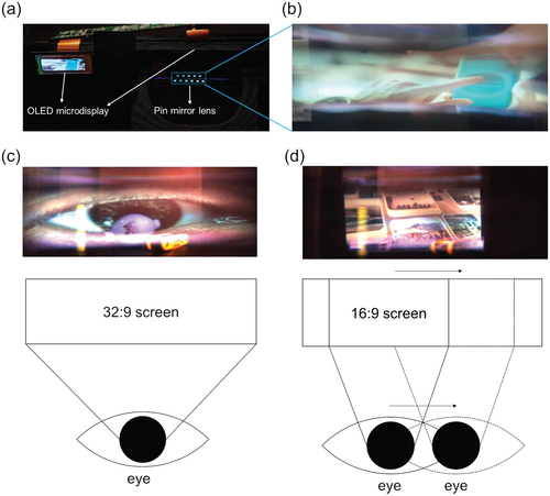
Figure (a) shows the OLED microdisplay panel combined with LetinAR’s pin mirror lens. The microdisplay is located on top of the lens, and the image generated from that is reflected by the pin mirrors, projected to the eye. Our AR device does not need additional optical components to become glass-like, as shown in Figure (b). For the small form factor device, the lens thickness, which determines the vertical FoV, was designed to be 4 mm, and the pin mirrors are laterally expandable. Therefore, the horizontal FoV can be expanded if the corresponding microdisplay width increases. Due to the high aspect ratio of the microdisplay, the AR device achieved the wide horizontal FoV of 46° with the lens thickness of 4 mm. The vertical FoV was measured as 5.5°, which resulted in a diagonal FoV of 46.3°. The relatively narrow vertical FoV was partly due to the high directivity of the OLED caused by the microcavity effect combined with the narrow rectangular collimator structure of the pin mirror lens. As the pin mirror lens was designed by assuming the Lambertian light source, some light emitted far from the center of the lens could not reach the narrow collimator if the light source has high directivity, which decreases the vertical FoV. Reducing the directivity by using a highly transparent top electrode can help to improve the vertical FoV. Figure (c) and (d) show examples of an AR device with a high aspect ratio microdisplay panel. By fully utilizing the 32:9 display panel with a 32:9 video source, as shown in Figure (c), the device can provide a wide horizontal FoV. On the other hand, with a common 16:9 video source, the device can provide an adequate FoV with a digital IPD adjustment by assigning a non-operating region to which the location of the screen can be shifted according to the IPD, as shown in Figure (d). To match the display center with the wearer’s pupil center, an additional mechanical slider may be needed, which would increase the form factor of the AR device. If the aspect ratio of the video source is 16:9 and if its resolution is 960 × 540, another 960 × 540 pixels would remain unused on a 32:9 screen that has 1920 × 540 pixels. The 16:9 video can be displayed by using 1–960 columns or 961–1,920 columns, which would result in a digital shift. For example, for a wearer with a narrow IPD, the left display uses 960-1,920 columns and the right display uses 1–960 columns. On the other hand, for a wearer who has an average IPD, both displays use 480-1,440 columns, and the 16:9 video is shown at the center of the display. Thus, without an additional mechanical slider, the device can match the center of the wearer’s pupils with the center of the 16:9 images.
Figure 5. (a) The OLED microdisplay combined with the pin mirror lens. (b) Image of the glass-like AR device using the OLED microdisplay and the pin mirror lens. (c) Operating image with the 32:9 aspect ratio, for which the video source fully utilizes the whole display panel. (d) Operating image with the common 16:9 aspect ratio, for which the screen is adjustable according to the IPD by using the non-operating region in the display panel.
4. Conclusion
In this study, we developed a color OLED microdisplay with a 32:9 aspect ratio. To protect the OLED from the moisture, oxygen, and solvents used in the subsequent patterning process, low-temperature processed bi-layered TFE (Al2O3/SiNx) was adopted. The OLED was not significantly degraded after the TFE and the patterning process. To implement C/F patterning on the OLED, a low-temperature C/F process was also developed. The C/F was properly formed on the OLED, which enabled successful demonstration of the color OLED microdisplay. By combining the OLED microdisplay with LetinAR’s pin mirror lens, the AR device showed a wide FoV with a small form factor. As we are developing low-temperature processable C/F materials, we will demonstrate a more vivid OLED microdisplay with a high color quality in the near future.
Acknowledgments
This study was partly supported by a grant from the Institute of Information & Communications Technology Planning & Evaluation (IITP) funded by the Korean government through the Ministry of Science and ICT (No. 2018-0-01035, Development of an Augmented Reality-based Life Safety Content Service Platform for Low Vision) and by a grant from the Electronics and Telecommunications Research Institute (ETRI) funded by the Korean government (21ZB1200).
Disclosure statement
No potential conflict of interest was reported by the author(s).
Additional information
Funding
Notes on contributors
Chan-mo Kang
Chan-mo Kang received his B.S. and Ph.D. in Electrical and Computer Engineering degrees from Seoul National University (SNU) in 2008 and 2014, respectively. He is currently a senior researcher at the Electronics and Telecommunications Research Institute (ETRI). His research interests include device engineering and physics in organic electronics, thin-film transistors (TFTs), and organic/inorganic hybrid devices.

Jin-Wook Shin
Jin-Wook Shin received his B.S. and M.S. degrees from Myongji University and Kwangwoon University, respectively. In 2018, he received his Ph.D. degree from Tohoku University in Japan. He joined ETRI in 2009. His current research interests include flexible organic light-emitting diode (OLED) displays with graphene films, microdisplays for augmented reality / virtual reality (AR/VR), and implantable biomedical devices.

Sukyung Choi
Sukyung Choi received her B.S. in Nanomaterials Engineering degree from Pusan National University, South Korea in 2011 and her Ph.D. in Chemistry degree from the Pohang University of Science and Technology (POSTECH) in 2016. She is currently a senior researcher at ETRI. Her current research interests are optoelectronic devices with quantum dots (QDs) and organics such as quantum light-emitting diodes (QLEDs) and OLEDs.

Byoung-Hwa Kwon
Byoung-Hwa Kwon received his B.S., M.S., and Ph.D. degrees from the Department of Materials Science & Engineering of Hanyang University in Seoul, South Korea in 2006, POSTECH in 2008, and KAIST in 2012, respectively. After graduating, he worked at the Department of Materials Science & Engineering of the University of Florida in Gainsville, U.S.A. as a postdoctoral associate and at LG Chem Ltd. as a senior researcher. He has been a senior researcher at ETRI since 2014. His current research interests are optoelectronic materials and devices such as OLEDs and quantum dot light-emitting diodes (QD-LEDs), and thin-film encapsulation for flexible devices.

Hyunsu Cho
Hyunsu Cho received his B.S. and Ph.D. in Electrical Engineering degrees from KAIST in Daejeon, South Korea in 2008 and 2014, respectively. He joined ETRI in Daejeon, South Korea in 2014, where he is currently a senior researcher. His research interests include the device physics and optical design of optoelectronic devices such as OLEDs.
Nam Sung Cho
Nam Sung Cho received his B.S. degree from Chung-Ang University in Seoul, South Korea in 2000, and his M.S. and Ph.D. in Chemistry degrees from KAIST in 2002 and 2006, respectively. From 2006 to 2008, he was a postdoctoral associate at the University of California Santa Barbara. He worked on materials development for OLEDs at LG Display R&D Center in Paju from 2008 to 2011. He joined ETRI in 2011. His current research interests include the OLED structure, OLED materials, and white OLEDs.
Jeong-Ik Lee
Jeong-Ik Lee received his B.S., M.S., and Ph.D. in Chemistry degrees from KAIST in 1992, 1994, and 1997, respectively. After graduating, he joined the IBM Almaden Research Center in San Jose, CA, U.S.A. as a postdoctoral associate, and worked on organic light-emitting materials. He moved to ETRI in 1999 and continued his research on organic light-emitting materials and devices. He has led the Reality Devices Research Division of ETRI since 2017 and has been working on the convergence of display and sensor technologies.
Hyunkoo Lee
Hyunkoo Lee received his B.S. and M.S. in Electrical Engineering degrees from SNU in 2004 and 2006, respectively. From 2006 to 2009, he was a junior researcher in the Monitor Circuit Design Team of LG Display. He received his Ph.D. in Electrical Engineering degree in 2013, also from SNU. From 2013 to 2020, he was a senior researcher in the Reality Display Research Section of ETRI. He has been with Sookmyung Women’s University as an assistant professor since 2020. His research interests include the device physics of organic semiconductors and organic/inorganic hybrid materials, and their applications to optoelectronic devices such as OLEDs, QD-LEDs, and printed electronics. His current research interests are optoelectronic devices with non-metal transparent electrodes, thin-film encapsulation for flexible devices, and microdisplays for AR/VR.

Jeong Hwan Lee
Jeong-Hwan Lee received his B.S. and M.S. in Electronic Engineering degrees from Korea University in Seoul, South Korea in 1997 and 1999, respectively. He worked at Hynix Semiconductor from 1999 to 2002 and at Integrant Technology (merged with Analog Devices) from 2002 to 2009. He has been with RAONTECH since 2013 as a principal circuit designer.

Hokwon Kim
Hokwon Kim received his B.S. degree from Korea University in 2005. He is currently a senior engineer at the RAONTECH Research and Development Group.
Ara Cho
Ara Cho received her B.S. and M.S. in Electrical and Electronic Engineering degrees from Kangwon National University in 2011 and 2013, respectively. She is currently a senior design engineer at the RAONTECH Research and Development Group.

Sang Hyun Park
Sanghyun Park received his B.S. and M.S. in Electronic Engineering degrees from Korea University in Seoul, South Korea in 2017 and 2019, respectively. He is currently a junior engineer at the RAONTECH Research and Development Group.

Minseok Kim
Min-Seok Kim received his B.S. and M.S. in Electrical Engineering degrees from Korea University in 1990 and 1992, respectively, and his Ph.D. in Electrical Engineering degree from Dankook University in 2011. He was the key engineer at Samsung SDI’s Iljin Display, developing display driving circuits, HTPS TFT LCDs, and LCoS display modules for microdisplay applications. Since 2012, he has been the head of the Research and Development Group of RAONTECH. He oversees the engineering departments and focuses on developing microdisplay technologies for AR devices.
Soon-gi Park
Soon-gi Park has been a principal engineer at LetinAR since 2018. He received his B.S. and M.S. in Information Display degrees from Kyung Hee University in 2009 and 2011, respectively. He received his Ph.D. in Electrical Engineering and Computer Science degree from SNU in 2015. Before joining LetinAR, he was the senior research scientist of the Korea Institute of Science and Technology (KIST) from 2017 to 2018, and a post-doctoral researcher of the Tokyo University of Agriculture and Technology from 2015 to 2016. His research interests include optical design and evaluation of AR devices.
Youngjoon Kim
Youngjoon Kim received his B.S. in Electrical Engineering degree from the University of Seoul in 1992. After graduation, he developed switch, radio control unit, and mobile service platforms for 2G/3G networks at SK Holdings. He is currently the general manager of LetinAR.
Jeonghun Ha
Jeonghun Ha received his B.S. degree from Hongik University in 2016. He is currently the chief technology officer (CTO) of LetinAR.

Jaehyeok Kim
Jaehyeok Kim received his B.S. degree from Hanyang University in 2019. He is currently the chief executive officer of LetinAR.
Sang Tae Kim
Sangtae Kim received his B.S. and M.S. in Chemical Engineering degrees from Dankook University in 1990 and 1992, respectively, and his Ph.D. in New Materials Engineering degree from KAIST in 1997. He is currently the CTO of Dongwoo Fine-Chem.
Jong Soo Lee
Jongsoo Lee received his B.S. in Chemical Engineering degree from Young-Nam University in 1996, and his M.S. and Ph.D. in Display Engineering degrees from Chiba University in Japan in 1999 and 2002, respectively. He is currently a group leader at the Dongwoo Fine-Chem Color R&D Center.
Seung No Lee
Seungno Lee received his B.S. in Polymer Engineering degree from the Kum-Oh National University in South Korea in 2000, and his M.S. in Polymer Engineering degree from Sungkyunkwan University in South Korea in 2002. He is currently a researcher at the Dongwoo Fine-Chem Color R&D Center.

Yu Bin Im
Yubin Im received her B.S. and M.S. in Chemical Engineering degrees from Jeonbuk National University in South Korea in 2011. She is currently a researcher at the Dongwoo Fine-Chem Color R&D Center.
Chun-Won Byun
Chunwon Byun received his B.S. and M.S. in Electrical and Computer Engineering degrees from Hanyang University in 2002 and 2007, respectively. From 2007 to 2010, he worked at ETRI, and from 2011 to 2013, at Samsung Display in South Korea. Since 2013, he has been working as a senior researcher at the Reality Device Research Division of ETRI. His research interests include microdisplays for AR/VR, driving methods for new displays, and implantable biomedical devices.
References
- Y. Motoyama, K. Sugiyama, H. Tanaka, H. Tsuchioka, K. Matsusaki, and H. Fukumoto, High-efficiency OLED microdisplay with microlens array, J. Soc. Inf. Disp 27, 354 (2019).
- H. Lee, H. Cho, C.-W. Byun, C.-M. Kang, J.-H. Han, J.-I. Lee, H. Kim, J.H. Lee, M. Kim, and N.S. Cho, Device Characteristics of Top-Emitting Organic Light-Emitting Diodes Depending on Anode Materials for CMOS-Based OLED Microdisplays, IEEE Photonics J 10 (6), 8201809 (2018).
- J.-S. Na, S.-K. Hong, and O.-K. Kwon, A 4410-ppi Resolution Pixel Circuit for High Luminance Uniformity of OLEDoS Microdisplays, IEEE J. Electron Devices Soc 7, 1026 (2019).
- M.-U. Erdenebat, Y.-T. Lim, K.-C. Kwon, N. Darkhanbaatar, and N. Kim, Waveguide-Type Head-Mounted Display System for AR Application. In State of the Art Virtual Reality and Augmented Reality Knowhow; Mohamudally, N., Ed.; IntechOpen: London, UK, 2018; pp. 41–58
- Soon-gi Park, PinMR: From Concept to Reality (Conference Presentation), Proc. SPIE 11310, Optical Architectures for Displays and Sensing in Augmented, Virtual, and Mixed Reality (AR, VR, MR), 113102J (2020)
- S. Kim, M. Kim, S. Lee, J. Song, S. Tamura, S. Kang, J. Kim, S. Cho, J. Cho, M. Suh, and H. Kim, 61.3: 3.0-in. 308-ppi WVGA AMOLED by Top-Emitting White OLED with Color Filter, SID Symposium Digest of Technical Papers 39, 937 (2008)
- M. Noda, K. Teramoto, E. Fukumoto, T. Fukuda, K. Shimokawa, T. Saito, T. Tanikawa, M. Suzuki, G. Izumi, S. Kumon, T. Arai, T. Kamei, M. Kodate, S. No, T. Sasaoka, and K. Nomoto, 74.1L: Late-News Paper: Oxide TFTs and Color Filter Array Technology for Flexible Top-emission White OLED Display, SID Symposium Digest of Technical Papers 43, 998 (2012).
- T. Fujii, C. Kon, Y. Motoyama, K. Shimizu, T. Shimayama, T. Yamazaki, T. Kato, S. Sakai, K. Hashikaki, K. Tanaka, and Y. Nakano, 4032 ppi High-resolution OLED microdisplay, J. Soc. Inf. Disp 26/3, 178 (2018).
- Y. Okaniwa, H. Tamura, M. Kibune, D. Yamazaki, T.-S. Cheung, J. Ogawa, N. Tzartzanis, W.W. Walker, and T. Kuroda, A 40-Gb/s CMOS Clocked Comparator With Bandwidth Modulation Technique, IEEE J. Solid-State Circuit 40 (8), 1680 (2005).
- J.-L. Huang, Y.-C. Liu, K.-C. Liang, Y.-H. Wang, C.-W. Yeh, Y.-R. Fang, Y.-Y. Huang, C.-E. Wu, Y.-T. Liu, and C.-W. Kang, P-60: An 8Gbps Receiver for 8 K Large-Size Display, SID Symposium Digest of Technical Papers 50, 1460 (2019).
- U. Vogel, P. Wartenberg, B. Richter, S. Brenner, K. Fehse, and M. Schober, OLED-on-Silicon Microdisplays: Technology, Devices, Applications, Proc. Eur. Solid-State Device Res. Conf. 2018, 90.
- H. Lee, H. Cho, C.-W. Byun, C. Kang, J.-W. Shin, S. Choi, B.-H. Kwon, N.S. Cho, A. Cho, H. Kim, J. Cho, S.H. Park, M. Kim, S. Park, Y. Kim, J. Ha, and J. Kim, 12-3: Organic Light-emitting Diode Microdisplay with a 32:9 Aspect Ratio for Wide Field of View, SID Symposium Digest of Technical Papers 51, 153 (2020).
- J.S. Park, H. Chae, H.K. Chung, and S.I. Lee, Thin film encapsulation for flexible AM-OLED: A review, Semicond. Sci. Technol 26, 034001 (2011).
- T. Davidson-Hall, and H. Aziz, A comparison of the effect of joule heating vs thermal annealing on the morphology of typical hole transport layers in organic light emitting devices, Proc. of SPIE 9566, 956621 (2015).
- S. Krotkus, F. Ventsch, D. Kasemann, A.A. Zakhidov, S. Hofmann, K. Leo, and M.C. Gather, Photo-patterning of Highly Efficient State-of-the-Art Phosphorescent OLEDs Using Orthogonal Hydrofluoroethers, Adv. Opt. Mater 2 (11), 1043 (2014).
- H. Cho, C.-W. Byun, C.-M. Kang, J.-W. Shin, B.-H. Kwon, S. Choi, N.S. Cho, J.-I. Lee, H. Kim, J.H. Lee, M. Kim, and H. Lee, White organic light-emitting diode (OLED) microdisplay with a tandem structure, J. Inf. Disp 20 (4), 249 (2019).