
ABSTRACT
Based on the movement and accumulation of ions in the 1-ethyl-3-methylimidazolium dicyanamide ([EMIM]DCA) electrolyte under a positive gate bias, the electrical double layer (EDL) was formed between a nanomesh channel and the [EMIM]DCA electrolyte to contribute to the increase in the conductance of the channel. The basic functions of artificial synapses, such as excitatory postsynaptic current (EPSC), paired pulse facilitation (PPF), short-term plasticity (STP), and long-term plasticity (LTP), are realized successfully. Besides, the high-pass filter function was implemented, which shows the application potential of the device in signal processing.
1. Introduction
With the advent of the big data era, memory capacity is increasing exponentially. The data transfer bandwidth between the central processing unit and the memory creates a bottleneck in the computing speed, which is called a ‘von Neumann bottleneck’ [Citation1]. Inspired by the working patterns of the human brain, researchers are trying to overcome the von Neumann bottleneck’ by building neuromorphic computing systems based on artificial synapses for parallel data processing [Citation2,Citation3]. The biological synapse is a functional junction that connects a pair of neurons. Information storage and processing are performed simultaneously or consecutively in the same synapses by tuning the synaptic weight [Citation4]. As a rising technology, synaptic electronics has attracted further attention due to its ability to mimic the structure and functions of biological counterparts [Citation5–8]. A number of synaptic devices have been intensively studied for their neuromorphic system, such as artificial neural networks, which are the next-generation energy-efficient computing method [Citation9,Citation10]; artificial tactile-perception systems, which have a similar function as a biological reflection arc [Citation11,Citation12]; and artificial visual-perception systems [Citation13,Citation14]. As artificial synapses, electrolyte-gated synaptic transistors (EGSTs) can mimic the basic synapse-like functions by forming and dissipating the electrical double layer (EDL). In this study, magnesium-doped indium oxide (Mg-InOx) nanomesh-based electrolyte-gated synaptic transistors (NEGSTs) were introduced. Compared with the traditional semiconductor film, the nanomesh has an enormous surface area that facilitates full contact and reaction with the 1-ethyl-3-methylimidazolium dicyanamide ([EMIM]DCA) electrolyte, thereby amplifying the effect of the EDL. When the gate voltage is applied, the conductivity of the Mg-InOx nanomesh channel changes significantly and rapidly due to the formation and dissipation of the EDL. Electrospun Mg-InOx NEGSTs have outstanding sensitivity and low operating voltage compared with metal oxide film-based synaptic transistors, as shown in Table , which can respond to a gate pulse with a duration of only 10 ms, with the amplitude of the pulse only 1 V and the read voltage applied (Vds) only 0.1 V. The device exhibits favorable synaptic performance by applying a pulse gate voltage with different parameters [Citation19].
Table 1. Performance comparison of synaptic transistors with different channel materials and channel structures.
2. Experiment
2.1. Preparation of the indium chloride precursor solution
First, indium chloride (InCl3) and magnesium chloride (MgCl2) precursors were fully dissolved in 2-Methoxyethanol at room temperature to obtain a InCl3 0.1 mol/L and MgCl2 0.05 mol/L solution. Here, doped magnesium was used as an oxygen absorber that can combine better with oxygen atoms, reduce the oxygen vacancy concentration, and then reduce the carrier concentration, to reduce the off-state current and improve the performance of the device [Citation20]. Next, 10 wt% polyvinyl pyrrolidone (PVP) powder was added to the precursor solution to increase its viscosity. The solution was stirred for 12 h under ambient conditions to make it uniform and transparent, as shown in Figure (a). Finally, the solution was aged for 24 h at room temperature.
Figure 1. (a) Mg-InOx precursor solution. (b) [EMIM]DCA ionic liquid and the ion composition. (c) Fabrication process of Mg-InOx nanomesh-based electrolyte-gated synaptic transistors (NEGSTs).
![Figure 1. (a) Mg-InOx precursor solution. (b) [EMIM]DCA ionic liquid and the ion composition. (c) Fabrication process of Mg-InOx nanomesh-based electrolyte-gated synaptic transistors (NEGSTs).](/cms/asset/fce5ed6a-e140-47a7-ac13-bf3469517054/tjid_a_1911866_f0001_oc.jpg)
2.2. Fabrication and characterization of the nanomesh-based synaptic
Boron-doped silicon with 120 nm thermally grown silicon oxide was used as the substrate. The InCl3/MgCl2/PVP nanomesh was deposited on the substrate using the electrospinning method with an electrohydrodynamic (EHD) jet printing equipment, the eNano Jet Printer ENJET. The distance between the nozzle and the substrate was 20 cm and the applied voltage was 5 kV. The electrospun InCl3/MgCl2/PVP nanomesh was irradiated with ultraviolet light (wavelength: 185–254 nm) for 30 min for the preliminary decomposition of the PVP and to help reduce the subsequent annealing temperature [Citation21,Citation22]. Then the nanomesh was annealed at 450°C for 1 h to form the Mg-InOx nanomesh channel. Next, the aluminium source and drain (S/D) electrodes were deposited by sputtering. Finally, the [EMIM]DCA ionic liquid was dripped between the S/D electrodes to serve as the electrolyte gate that is full of anions and cations and had high viscosity, as shown in Figure (b). The entire fabrication process of the NEGSTs is shown in Figure (c).
3. Results and discussion
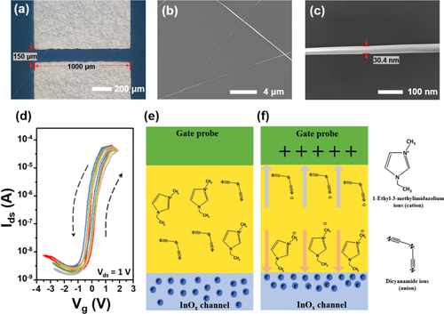
Figure (a) shows optical microscope images of the Mg-InOx nanomesh channel. The channel area formed after the deposition of the electrodes was 150 μm long and 1,000 μm wide. Figure (b) and (c) show the SEM images of the Mg-InOx nanomesh at different resolutions. The electrospun Mg-InOx nanomesh had a nanoscale diameter (∼30 nm) that showed a tremendous surface area, which was helpful for fully contacting and reacting with the [EMIM]DCA electrolyte under the applied gate bias. Because the Mg-InOx nanomesh was randomly distributed in the region between the S/D electrodes, it was difficult to estimate the width and length of the channel. Therefore, we approximated the width and length of the channel by using its geometrical width and length (the region between the S/D electrodes). The geometrical width was the maximum value of the nanomesh width, and the geometrical length was the minimum value of the nanomesh length. Figure (d) shows the hysteresis curves of the Mg-InOx NEGSTs with the gate voltage (Vg) directly applied on the [EMIM]DCA electrolyte. The channel current (Id) was measured by applying a small read voltage (Vds = 1 V) between the S/D electrodes. The device showed counterclockwise hysteresis with high/low conductance changes at the average rate of about 200% at Vg = 0 V in five consecutive measurements. After multiple measurements, the hysteresis curve of the device was not significantly degraded, thereby showing good repeatability. The hysteretic behavior indicates a non-volatile change of the Mg-InOx nanomesh channel conductance, which is essential for the implementation of the synaptic functionality [Citation22–25]. The observed hysteretic behavior can be understood based on the formation and dissipation of the EDL on the interface between the [EMIM]DCA electrolyte and the Mg-InOx nanomesh channel [Citation26]. A schematic of the process is shown in Figure (e) and (f). In the initial state, the 1-Ethyl-3-methylimidazolium cations ([EMIM]+) and the dicyanamide anions (DCA-) in the electrolyte were evenly distributed. When a positive bias was applied on the electrolyte gate, the [EMIM]+ were driven toward the channel and then accumulated at the interface between the [EMIM]DCA electrolyte and the Mg-InOx nanomesh channel, which caused the electrons in the channel to also accumulate at the interface. Meanwhile, the EDL was formed, which increased the conductance of the Mg-InOx nanomesh channel. When the gate voltage was lowered from the upper limit, the internal field built by the concentration gradient of the ions in the [EMIM]DCA electrolyte became gradually dominant and drove the [EMIM]+ that accumulated on the channel surface back into the electrolyte. When the negative gate voltage reached −2 V, the [EMIM]+ were fully extracted out of the EDL, and then the conductance of the Mg-InOx nanomesh channel was restored to its initial value.
Figure 2. (a) Optical microscope images of the Mg-InOx nanomesh channel. (b) and (c): SEM images of the Mg-InOx nanomesh at different resolutions. (d) Hysteresis curves of the Mg-InOx nanomesh-based electrolyte-gated synaptic transistors (NEGSTs). The distribution of the ions and electrons (e) without and (f) with applied positive gate bias.
To investigate the behavior of the ions in the [EMIM]DCA electrolyte, the frequency-dependent capacitance of the electrolyte is shown in Figure (a). As the frequency increases, the effective capacitance drops, which is due to the slow ion mobility in the response to the high electric-field frequency. The effective capacitance at 10 kHz remained about 0.5 μFcm−2. The high effective capacitance of the electrolyte is attributed to the formation of the EDL at the electrolyte/electrode interface. The ionic conductive property of the electrolyte made possible the construction of the synaptic transistors. Figure (b) shows the excitatory postsynaptic current (EPSC) of the Mg-InOx NEGSTs under the condition of the applied gate voltage. A series of pulse voltages with the same duration (10 ms) and different amplitudes (1, 2, and 3 V) were applied on the electrolyte gate as external action potentials, and the EPSC was measured using a fixed read voltage (Vds = 0.1 V). When the positive voltage was applied to the electrolyte gate, the cations in the electrolyte gathered on the surface of the Mg-InOx nanofibers due to the repulsion force, and then the electrons in the Mg-InOx nanofibers also accumulated at the electrolyte/nanofibers interface, induced by the aggregated cations. At this time, the EDL formed at the interface and increased the conductivity of the Mg-InOx nanofibers. After the gate voltage was removed, due to the existence of a concentration difference, the cations and electrons that gathered at the EDL slowly returned to the electrolyte and the Mg-InOx nanofiber, respectively. The conductivity of the Mg-InOx nanomesh channel gradually returned to its initial state. The EPSC reached its peak value at the end of the input pulse, which increased with the increase in the pulse gate voltage amplitude and then decremented. This behavior is similar to that observed in bio-excitatory synapses [Citation27]. As the pulse amplitude increased to 2 and 3 V, the EPSC did not decay back to the initial current value, which indicates that the device is non-volatile. Figure (c) shows the channel conductance change realized by a pair of voltage pulses (2 V, 10 ms) with an input interval (Δt) of 40 ms. After the first pulse gate voltage stimulation, the EDL was formed at the interface between the electrolyte and the nanofibers, and the conductivity of the Mg-InOx nanomesh channel increased. After the gate voltage was removed, the cations and electrons that gathered at the EDL gradually returned to their initial position, which caused the EDL to dissipate gradually and reduced the conductivity of the Mg-InOx nanomesh channel. Before the EDL completely dissipated, a second forward pulse voltage was applied to the electrolyte gate, which caused more cations and electrons to gather at the interface, thereby forming a stronger EDL, and further improved the conductivity of the Mg-InOx nanomesh channel. Therefore, the peak value of the channel conductance excited by the second pulse was greater than that of the channel conductance excited by the first pulse. The paired pulse facilitation (PPF) index is defined as the ratio of the amplitude of change between the first EPSC value (A1) and the second EPSC value (A2), drawn as the function of Δt in Figure (d), where the PPF index decreased with the increase in the Δt.
Figure 3. (a) Specific capacitance as a function of the frequency of the [EMIM]DCA electrolyte. (b) Excitatory postsynaptic current (EPSC) under different amplitude gate pulses. (c) Paired-pulse facilitation (PPF). (d) PPF index dependent on the time interval.
![Figure 3. (a) Specific capacitance as a function of the frequency of the [EMIM]DCA electrolyte. (b) Excitatory postsynaptic current (EPSC) under different amplitude gate pulses. (c) Paired-pulse facilitation (PPF). (d) PPF index dependent on the time interval.](/cms/asset/c1071c08-9d1c-4d5a-9556-a3250c556141/tjid_a_1911866_f0003_oc.jpg)
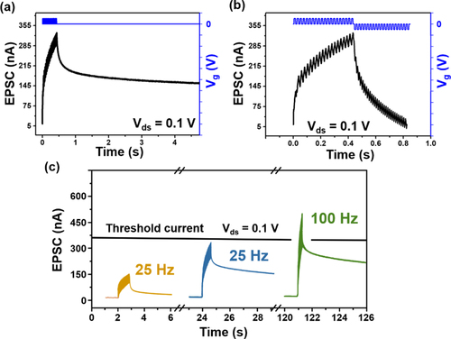
For the implementation of the long-term memory, it is necessary to achieve the long-term plasticity (LTP) property. The LTP of the Mg-InOx NEGSTs is shown in Figure (a). After 20 pulses (1 V, 10 ms) at 10 ms intervals, the increases in the EPSC after each pulse were measured. An obvious non-volatile channel current was obtained, which indicates a non-volatile change in the channel conductance that is meaningful for the formation of long-term memories. An analog switch was obtained by alternately applying 20 identical pulses (±1 V, 10 ms) at 10 ms intervals, as shown in Figure (b). The increase and decrease in the channel conductance can be regarded as the long-term potentiation (LTP) and the long-term depression (LTD) of the artificial synapse, respectively. The biological synapse can act as a dynamic filter for processing input information, depending on the frequency of the excitation. In biological neuromorphic networks, synapses with a low probability of initial vesicle release can act as high-pass filters that use only high-frequency signals to trigger vesicle release [Citation28]. To demonstrate the high-pass filter behavior of Mg-InOx NEGSTs, various presynaptic spikes with different frequencies were applied to the electrolyte gate (25, 50, and 100 Hz), as shown in Figure (c). The EPSC was recorded with Vds = 0.1 V. A baseline that was defined as the threshold current was set at the current value of 350 nA. That the EPSC value was lower than the threshold current can mean that there was no signal output from the high-pass filter. The EPSC higher than the set threshold current means that the signal from the presynaptic spikes passed the device. There was no significant change in the EPSC amplitude after 20 presynaptic peaks with a frequency of 25 Hz. With the increment in the presynaptic spike frequency, the EPSC amplitudes dramatically increased. The EPSC was kept under the threshold current when the frequency was increased to up to 50 Hz. When the frequency of the presynaptic spikes was fixed at 100 Hz, the Mg-InOx NEGSTs exhibited a higher EPSC value than the threshold current, which proved the high-pass filtering behavior of our device [Citation29].
Figure 4. (a) Long-term plasticity of the Mg-InOx nanomesh-based electrolyte-gated synaptic transistors (NEGSTs). (b) Analog switch realized by alternately applying 20 identical pulses (±1 V, 10 ms) at 10 ms intervals. (c) Amplitude of the excitatory postsynaptic current (EPSC) in response to 20 presynaptic spikes with various frequencies.
4. Conclusion
Mg-InOx NEGSTs were fabricated successfully through the solution process wherein an electrospun Mg-InOx nanomesh was used as the channel and the [EMIM]DCA ionic liquid was used as the electrolyte gate. Thanks to its enormous surface area, the nanomesh channel can come in contact with the electrolyte and react more fully under the applied positive gate bias and generate an EDL at their interface that can increase the conductance of the channel. The short-term plasticity and long-term plasticity of the device were achieved successfully by applying different amplitudes and frequencies of the gate pulse spikes. Based on the formation and dissipation of EDL, the basic functions of artificial synapses, including EPSC and PPF, were favorably realized. Our device also successfully simulated the function of the high-pass filter by inputting gate pulses with different frequencies and setting a threshold current, which showed the potential of the device for application in the field of signal processing. Therefore, this study is helpful for future studies on multifunctional artificial synapses and neuromorphic systems.
Disclosure statement
No potential conflict of interest was reported by the author(s).
Additional information
Funding
Notes on contributors

Wei Qin
Wei Qin is an M.S. candidate at the School of Electrical and Electronic Engineering of Yonsei University in Seoul, South Korea. He has been researching on synaptic transistors and metal oxide-based thin-film transistors.

Byung Ha Kang
Byung Ha Kang is a Ph.D. candidate at the School of Electrical and Electronic Engineering of Yonsei University in Seoul, South Korea. He has been researching on photo-sensors and solution-processed metal oxide-based thin-film transistors.

Jong Bin An
Jong Bin An is a Ph.D. candidate at the School of Electrical and Electronic Engineering of Yonsei University in Seoul, South Korea. He has been researching on IOT sensors and metal oxide-based thin-film transistors.

Hyun Jae Kim
Hyun Jae Kim received his Ph.D. degree from the Department of Materials Science and Engineering of Columbia University in New York, NY, USA in 1996. He has been a professor at the School of Electrical and Electronic Engineering of Yonsei University in Seoul, South Korea since 2005.
References
- P. Huang, J. Kang, Y. Zhao, S. Chen, R. Han, Z. Zhou, Z. Chen, W. Ma, M. Li, L. Liu, and X. Liu, Adv. Mater. 28, 9758–9764 (2016).
- H.L. Park, Y. Lee, N. Kim, D.G. Seo, G.T. Go, and T.W. Lee, Adv. Mater. 32, 1903558 (2020).
- S. Kim, B. Choi, M. Lim, J. Yoon, J. Lee, H.D. Kim, and S.J. Choi, ACS Nano 11, 2814–2822 (2017).
- G. Bi, and M. Poo, J. Neurosci. 18, 10464–10472 (1998).
- X. Wang, Y. Yan, E. Li, Y. Liu, D. Lai, Z. Lin, Y. Liu, H. Chen, and T. Guo, Nano Energy 75, 104952 (2020).
- M.J. Park, Y. Park, and J.S. Lee, ACS Appl. Electron. Mater. 2, 339–345 (2020).
- D. Jiang, J. Li, W. Fu, Q. Chen, Y. Yang, Y. Zhou, and J. Zhang, ACS Appl. Electron. Mater. 2, 2772–2779 (2020).
- J.T. Kim, J. Song, and C.S. Ah, ACS Appl. Electron. Mater. 2, 2057–2063 (2020).
- G.W. Burr, P. Narayanan, R.M. Shelby, S. Sidler, I. Boybat, C. di Nolfo, and Y. Leblebici, presented at the IEEE Int. Electron Devices Meeting (IEDM), Swiss federal Institute of Technology in Lausanne, Lausanne, Switzerland, 2015.
- E.J. Fullre, S.t. Keene, A. Melianas, Z. Wang, S. Agarwal, Y. Li, Y. Tuchman, C.D. James, M.J. Marinella, J.J. Yang, A. Salleo, and A.A. Talin, Science 364, 570–574 (2019).
- Y. Kim, A. Chortos, W. Xu, Y. Liu, J.Y. Oh, D. Son, J. Kang, A.M. Foudeh, C. Zhu, Y. Lee, S. Niu, J. Liu, R. Pfattner, Z. Bao, and T.W. Lee, Science 360, 998–1004 (2018).
- C. Zhang, W.B. Ye, K. Zhou, H.Y. Chen, J.Q. Yang, G. Ding, X. Chen, Y. Zhou, F. Li, and S.T. Han, Adv. Funct. Mater. 29, 1808783 (2019).
- S. Chen, Z. Lou, D. Chen, and G. Shen, Adv. Mater. 30, 1705400 (2018).
- H. Wang, Q. Zhao, Z. Ni, Q. Li, H. Liu, Y. Yang, L. Wang, Y. Ran, Y. Guo, W. Hu, and Y. Liu, Adv. Mater. 30, 1803961 (2018).
- Y. He, R. Liu, S. Jiang, C. Chen, L. Zhu, Y. Shi, and Q. Wan, J. Phys. D: Appl. Phys. 53, 215106 (2020).
- X. Liang, Z. Li, L. Liu, S. Chen, X. Wang, and Y. Pei, Appl. Phys. Lett. 116, 012102 (2020).
- F. Shao, Y. Yang, L.Q. Zhu, P. Feng, and Q. Wan, ACS Appl. Mater. Interfaces 8, 3050–3055 (2016).
- Y. He, J. Sun, C. Qian, L.A. Kong, G. Gou, and H. Li, Appl. Phys. A-Mater. Sci. Process. 123, 227 (2017).
- J. Zhou, C. Wan, L. Zhu, Y. Shi, and Q. Wan, IEEE Electron Device Lett. 34, 1433–1435 (2013).
- L. Song, L. Luo, X. Li, D. Liu, N. Han, L. Liu, Y. Qin, J.C. Ho, and F. Wang, Adv. Electron. Mater. 5, 1800707 (2019).
- Y.J. Tak, S.P. Park, T.S. Jung, H. Lee, W.G. Kim, J.W. Park, and H.J. Kim, J. Inf. Disp. 17, 73–78 (2016).
- S.C. Park, D. Kim, H. Shin, D.K. Lee, X. Zhang, J. Park, and J.S. Choi, J. Inf. Disp. 17, 1–7 (2016).
- Y. Burgt, E. Lubberman, E.J. Fuller, S.T. Keene, G.C. Faria, S. Agarwal, M.J. Marinella, A.A. Talin, and A. Salleo, Nat. Mater. 16, 414–418 (2017).
- J. Lenz, F. Giudice, F.R. Geisenhof, F. Winterer, and R.T. Weitz, Nat. Nanotechnol. 14, 579–585 (2019).
- Y. Park, M.K. Kim, and J.S. Lee, Carbon 165, 455–460 (2020).
- J. Jiang, Q. Wan, J. Sun, and A. Lu, Appl. Phys. Lett. 95, 152114 (2009).
- P. Sah, S. Hestrin, and R.A. Nicoll, J. Physiol. 430, 605–616 (1990).
- D. Liu, Q. Shi, S. Dai, and J. Huang, Small 16, 1907472 (2020).
- J. Zhou, N. Liu, L. Zhu, Y. Shi, and Q. Wan, IEEE Electron Device Lett. 36, 198–200 (2015).