
 ?Mathematical formulae have been encoded as MathML and are displayed in this HTML version using MathJax in order to improve their display. Uncheck the box to turn MathJax off. This feature requires Javascript. Click on a formula to zoom.
Abstract
This paper proposes a complementary metal–oxide–semiconductor (CMOS) amplifier using low-temperature poly-Si oxide (LTPO) thin-film transistors (TFTs). The Corbino structure used in the proposed amplifier has a higher output resistance than conventional amplifiers. The proposed circuit is composed of two CMOS inverters, one CMOS switch, and one input capacitor. It was possible to determine the operating point where the voltage gain could be kept high, regardless of the device variation, by shorting the gate input and output of the first amplifier. The alternating current component of the input signal was increased because the input signal was transferred to the first amplifier via the capacitor. The function of the second amplifier was to increase the total voltage gain. When a peak-to-peak voltage sine wave of 2 mV was applied at a frequency lower than 500 Hz, the proposed circuit showed an average voltage gain of 60.6 dB, which is the highest among the previously published TFT amplifiers.
1 Introduction
Currently, various backplane technologies have been used in display applications. For instance, thin-film transistors (TFTs) made of n-type hydrogenated amorphous silicon (a-Si:H) have been widely used in liquid crystal display panels. TFTs made of low-temperature polycrystalline silicon (LTPS) exhibit high mobility, thereby allowing for high-speed operation. N-type amorphous indium-gallium-zinc oxide TFTs, also known as oxide TFTs, have extremely low leakage currents and uniform device performance. LTPS and oxide TFT technologies have been widely used in mobile and large area displays, respectively. Recently, low-temperature poly-Si oxide (LTPO) TFT technologies have been actively studied for mobile applications [Citation1]. The low leakage current of oxide TFT contributes to the realization of a variable refresh rate and low power consumption in display applications. As a result, various studies adopting the LTPO technology have been conducted, such as pixel circuits for displays using organic light-emitting diodes [Citation2–5], liquid crystals [Citation6–9], and micro-light-emitting diodes [Citation10]. In addition to pixel circuits, LTPO technology has been studied in display circuits, such as gate drivers [Citation2,Citation11–13], level shifters [Citation14], and inverters [Citation15–19].
TFT-based amplifiers have become increasingly important as biometric data measurement via wearable devices has been actively studied [Citation20–25]. Biosignal measurement, such as electroencephalogram (EEG), has made it possible to evaluate emotion [Citation21–24] or stress [Citation25]. EEG signals have frequencies below 100 Hz and amplitudes in the order of microvolts [Citation26]. Therefore, an amplifier is required since the biosignals are remarkably weak. The amplifier must be located close to the signal source in order to amplify a small signal with less noise. Biosignals are detected on human skin or organs with uneven surfaces, indicating that a detection system implemented on a flexible substrate is the best solution. Therefore, flexible electronics have received a lot of attention [Citation27, Citation28]. TFT technology can be used to implement a biosignal acquisition system that includes amplifiers on a flexible substrate.
Among the TFT-based amplifiers, oxide TFT-based amplifiers have been continuously studied due to the advantages of oxide TFT such as low leakage current and low manufacturing cost. Voltage gains of complementary metal–oxide–semiconductor (CMOS) amplifiers using LTPO TFTs [Citation16–19] ranged from 36.7–50.7 dB. Pseudo CMOS amplifiers [Citation29, Citation30] exhibited voltage gains of 22.5 and 19.4 dB. It was reported that the voltage gain of an amplifier adopting n-type oxide TFTs was 23.52 dB [Citation31].
This paper proposes a new amplifier using LTPO TFTs with a Corbino structure. The circular-shaped Corbino TFT features a very high output resistance [Citation32], thus allowing for a high amplifier gain. The proposed amplifier adjusts the operating point of the inverting amplifier in order to amplify the signal regardless of the direct current (DC) component of the input signal. In addition, the proposed amplifier achieves a higher gain by connecting the two inverting amplifiers.
2 Proposed circuit
Figure shows the proposed circuit and timing diagram of the control signals. The proposed amplifier is composed of two CMOS inverting amplifiers (M1–M4), a CMOS transmission gate (M5, M6), and a capacitor (CIN). The output of the first amplifier, VOUT1, is connected to the input of the second amplifier. Since the input signal VIN enters CIN, the proposed amplifier can only amplify the alternating current (AC) signal regardless of the DC component.
Figure 1. (a) Circuit diagram of the proposed amplifier and (b) timing diagram.
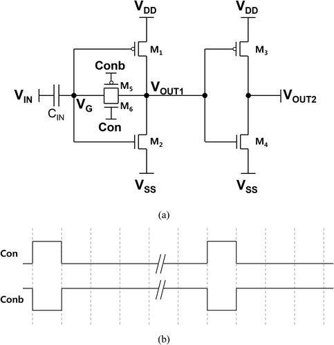
Switches M5 and M6 determine the input operating point of the first amplifier. The two control signals, Con and Conb, have opposite polarities, as shown in Figure (b). If both switches are turned on, VG and VOUT1 are connected.
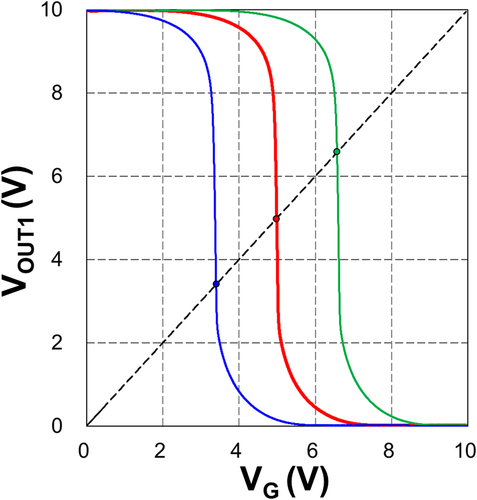
Figure shows the operating principle of the first amplifier. The red solid line represents the ideal transfer characteristics of the CMOS inverter. The green and blue lines are obtained by shifting the red solid line. Meanwhile, the black dashed line represents the relationship between VOUT1 and VG. VOUT1 = VG indicates that the inputs and outputs are shorted. The symbols shown in Figure are the intersections between the dashed line and the three colored lines. In particular, VG can be initialized by shorting the input and output of the amplifier. A small input signal is transferred through CIN, as shown in Figure (a). The DC operating voltage of VG must be determined before transferring the input signal. This can be accomplished by shorting VG and VOUT1. The voltage gain is also calculated as the slope at the intersection between the transfer curve and the dashed line. The stiffer the slope, the higher the voltage gain. Higher output resistances of M1 and M2 result in a stiffer slope. As such, we used Corbino structures for the amplifier TFTs. The variation in device characteristics causes a shift in the transfer curve, as shown in Figure . Shorting VG and VOUT1 may result in a high slope, as shown in Figure . Therefore, the proposed amplifier can amplify a signal with a high voltage gain regardless of inverter characteristics.
Figure 2. Determination of the operating point of the first amplifier by shorting the input and output.
The proposed circuit has an additional inverter amplifier connected to VOUT1. The second amplifier enhances VOUT1, which is the output of the first amplifier, thus achieving a significant voltage gain. VIN and VOUT2 are in phase when two inverting amplifiers are used.
3 Measurement results and discussion
The circuits were fabricated using an LTPO TFT process. The image on the left of Figure (a) shows the first amplifier with CIN and switches. The second amplifier, shown on the right, is a simple inverter. The proposed amplifier was implemented by connecting the VOUT1 of the first amplifier, as shown in Figure (a), to the input of the second inverter using two shorted probes.
Figure 3. (a) Micrograph of the fabricated circuit, and (b) measured output characteristics of the n-type Corbino TFT with (R1, R2) = (72, 57 µm) and conventional bar-type TFT with W/L = 50 µm / 10 µm, (c) transfer curve, and (d) output curves of the n-type Corbino TFT with (R1, R2) = (72, 57 µm) and p-type Corbino TFT with (R1, R2) = (25 µm, 10 µm).
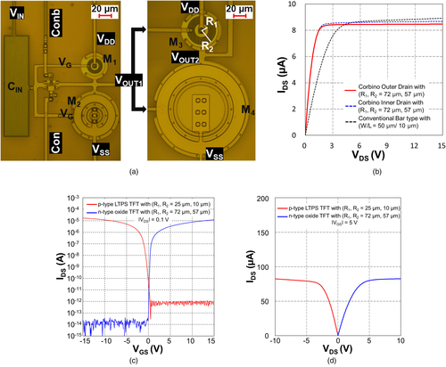
Figure (b) shows the output characteristics of oxide TFTs with Corbino and conventional structures when VGS is 2 V. R1 and R2 of the n-type Corbino TFT (M4) were 72 and 57 µm, respectively, in Figure (b), (c), and (d). The effective W/L of the Corbino TFT was 26.9. The W/L of the conventional TFT was 50 µm /10 µm. The red solid line and blue dashed line represent the drain currents of the outer and inner drain connections, respectively. An inner or outer drain indicates that the inner or outer circular electrode acts as a drain. The black dashed line shows the output characteristics of the conventional TFT. The measured output resistance ro of a conventional bar-type TFT was 42 MΩ. The measured ro of the Corbino TFT with an outer drain was 403 MΩ, which was higher than the inner drain with a value of 136 MΩ. The measurement results confirm that the Corbino TFT has a much higher ro than the conventional TFT. Figure (c) shows the measured transfer curves of the p-type LTPS and n-type oxide TFTs with a Corbino structure when = 0.1 V. Figure (d) shows the output curves when
= 5 V. The threshold voltages (VTH) of the p-type and n-type TFTs were −0.0 and 0.2 V, respectively. R1 and R2 of the p-type LTPS TFT were 25 and 10 µm, respectively, in Figure (c) and (d).
The circuit information for the proposed amplifier, as shown in Figure , is listed in Table . Transistors M1–M4 were of the Corbino type, whereas switching transistors M5 and M6 were of the conventional (bar type). The W/L ratio of the Corbino TFT was calculated by using the following equation [Citation33]:
(1)
(1) where R1 and R2 are the inner and outer radii of the corresponding TFT, respectively. The definitions of R1 and R2 are shown in Figure (a). The R1 and R2 values for each Corbino TFT are shown in parentheses in Table . The voltage range of the two control signals was from −5 to 10 V. The turn-on time of M5 and M6 was 200 µs.
Table 1. Design parameters of the manufactured circuit.
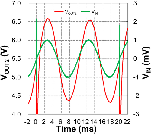
Figure shows the measurement results of the proposed amplifier when an input signal with a frequency of 100 Hz was applied. The red and green lines represent VOUT2 and VIN, respectively. The initialization of VG was conducted within 200 µs at 0 ms. The peak-to-peak voltage (VPP) of the VIN and VOUT1 were 2.1 and 18.7 mV, respectively. The VPP of VOUT2 was 2.26 V. As a result, the voltage gain of the proposed amplifier was 1091.5 V/V (60.8 dB). The voltage gains of the first and second amplifiers were −9.1 and −120.3 (V/V), respectively.
Figure 4. Measurement output of the proposed amplifier when a 100 Hz sine wave with 2 mV peak-to-peak was applied.
During the initialization period, the VG and VOUT1 were 5.24 V. Based on Figure , the voltage gain of the first amplifier is expected to be significantly high due to the 5.24 V operating point. However, the measured voltage gain of the first amplifier was −9.1 V/V because the AC component of the input signal, VIN, was not transmitted completely to the first amplifier. The actual voltage gain VG/VIN was less than one because of the input capacitances of M1 and M2. Therefore, the voltage gain of the first amplifier was only −9.1 V/V.
Figure 5. Measured transfer characteristics of the second amplifier and calculated voltage gain.
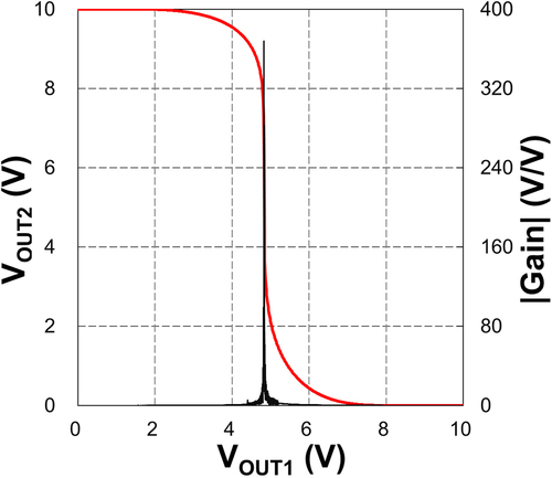
Figure 6. Measured voltage gain in dB depending on frequency.
A second amplifier can be used to compensate for this issue. The red line in Figure shows the measured voltage-transfer characteristics of the second amplifier. The black line indicates the calculated voltage gain, and it has the highest gain of −367.9 V/V when VOUT1 is 4.83 V.
Figure shows the voltage gain as a function of the signal frequency. When the VPP of the input signal was 2 mV, the proposed amplifier showed voltage gains of 60.1, 60.8, 60.0, 60.8, 61.3, 60.4, and 57.7 dB at frequencies of 10, 20, 50, 100, 200, 500, and 1,000 Hz, respectively. Despite a low power supply of only 10 V, the voltage gain of 61 dB was the highest among the previous studies on LTPO TFT amplifiers [Citation16–19].
The proposed amplifier features an LTPO process. The LTPO process is now available for flexible substrates. Furthermore, the amplifier adopts a Corbino structure and two-stage inverting amplifiers, which enable the highest voltage gain over previously published results. We believe that our amplifier can be used as a high-gain amplifier in a biosignal acquisition system implemented on uneven human skin.
5 Conclusion
A high-gain two-stage amplifier using LTPO technology was proposed. The proposed circuit is comprised of two CMOS inverter amplifiers, a CMOS switch, and an input capacitor. The voltage transfer characteristic exhibited a steep slope when using a Corbino-type TFT with a large output resistance of 403 MΩ. The first amplifier can be operated in the steep-slope region by shorting the input and output. Only a very small AC component of the input signal was amplified by using a two-stage inverter amplifier and an input capacitor. The measured voltage gain was 60.8 dB when a 100 Hz sine wave with a 2 mV VPP was applied. The proposed amplifier can be manufactured by using an LTPO process and integrated into wearable smart devices to measure biosignals.
Acknowledgement
This work was supported in part by the Basic Science Research Program through the National Research Foundation (NRF) under Grant NRF-2020R1I1A3A04037918 and in part by the BK21 FOUR Program through the Ministry of Education (MOE), South Korea. The EDA Tool was supported by the IC Design Education Center.
Disclosure statement
No potential conflict of interest was reported by the author(s).
Additional information
Funding
Notes on contributors

Dong-Hwan Jeon
Dong-Hwan Jeon received his BS and MS in information display at Kyung Hee University, Korea, in 2015 and 2017, respectively, where he is currently working toward his PhD in the Department of Information Display. He has been working on driving technology for the color and motion performance of OLEDs and microLEDs.

Won-Been Jeong
Won-Been Jeong received his BS degree in information display from Kyung Hee University, Seoul, Korea, in 2019, where he is currently pursuing master's degree with the Department of Information Display. His research interests include visual perception, and driving technology for low-power display.

Jeong-Soo Park
Jeong-Soo Park received his BS degree in information display from Kyung Hee University, Seoul, Korea, in 2022, where he is currently pursuing master's degree with the Department of Information Display. His research interests include visual perception, and driving technology for low-power display.

Hoon-Ju Chung
Hoon-Ju Chung received the B.S. degree in electrical engineering from Kyungpook National University, Daegu, South Korea, in 1994, and the M.S. and Ph.D. degrees from the Korea Advanced Institute of Science and Technology, Daejeon, South Korea, in 1997 and 2002, respectively. He is currently a Full Professor with the School of Electronic Engineering, Kumoh National Institute of Technology

Seung-Woo Lee
Seung-Woo Lee (SM’10) received the B.S. and M.S. degrees in electrical engineering and the Ph.D. degree from the Korea Advanced Institute of Science and Technology in 1993, 1995, and 2000, respectively, where he conducted research on integrated driver circuits for poly-Si TFT-LCDs. He joined Samsung in 2000, where his work has focused on the development of key driving technologies for active-matrix liquid-crystal displays. He has played a key role in image quality enhancement, high-end LCD timing-controller design, FPGA evaluation of new driving schemes, next-generation LCD interface technologies, and advanced LCD driving schemes for large-size TV applications. He was also in charge of the development of analog– digital mixed-signal ICs for TFT-LCDs. He joined Kyung Hee University, Seoul, South Korea, where he has been studying novel display systems and visual perception and is currently a Full Professor with the Department of Information Display. Prof. Lee was a recipient of the 2008 Chester Sall Award from IEEE Consumer Electronics Society in 2010. He has been active as a Senior Member of Society for Information Display since 2010.
References
- T.-K. Chang, C.-W. Lin, and S. Chang, presented at the SID Symposium Digest of technical papers (2019).
- H. Luo, S. Wang, J. Kang, Y. M. Wang, J. Zhao, T. Tsong, P. Lu, A. Gupta, W. Hu and H. Wu, presented at the SID Symposium Digest of Technical Papers, 2020.
- H. Qiu, J. An, K. Wang, C. Liao, C. Dai, X. Zhang, and S. Zhang, IEEE Journal of the Electron Devices Society 10, 51–58 (2022).
- J. Lee, D. Kim, J. Yang, K. Moon, S.Y. Lee, J. Jeon, Y. Kim, S. Choi, U. Chung, and K. Park, Journal of the Society for Information Display 28 (12), 1003–1011 (2020).
- J.C. Kim, J.S. Yoo, H.W. Hwang, H.C. Choi, Y.M. Ha, and H.J. Kim, presented at the 2021 28th International Workshop on Active-Matrix Flatpanel Displays and Devices (AM-FPD) (2021).
- M. Tada, K. Mochizuki, T. Tsunashima, H. Tanaka, T. Ito, H. Watakabe, A. Hanada, R. Kimura and Y. Ishii, presented at the SID Symposium Digest of technical papers, 2018.
- H. Watakabe, T. Jinnai, I. Suzumura, A. Hanada, R. Onodera, M. Tada, K. Mochizuki, H. Tanaka and T. Ito, presented at the SID Symposium Digest of technical papers, 2019.
- J. Kim, H.-J. Chung, and S.-W. Lee, IEEE Electron Device Letters 40 (12), 1957–1960 (2019).
- J. Kim, H.-J. Chung, and S.-W. Lee, IEEE Electron Device Letters 41 (6), 868–871 (2020).
- E. K. Jung, Y.-H. Hong, S. Hong, K. Park, S.-Y. Lee and Y.-S. Kim, presented at the SID Symposium Digest of Technical Papers, 2021.
- R. Yonebayashi, K. Tanaka, K. Okada, K. Yamamoto, K. Yamamoto, S. Uchida, T. Aoki, Y. Takeda, H. Furukawa, and K. Ito, Journal of the Society for Information Display 28 (4), 350–359 (2020).
- J. Kim, and J. Jang, Journal of the Society for Information Display (2022).
- J. Kim, Y. Chen, S. Lee, and J. Jang, IEEE Electron Device Letters 42 (11), 1619–1622 (2021).
- A. Rahaman, D.Y. Jeong, and J. Jang, IEEE Electron Device Letters 40 (11), 1772–1775 (2019).
- G. Jin, J. Choi, W. Lee, Y. Mo, H. Kim, S. Kim, M. Kim, and J. Song, IEEE electron device letters 32 (9), 1236–1238 (2011).
- C. Chen, B.-R. Yang, C. Liu, X.-Y. Zhou, Y.-J. Hsu, Y.-C. Wu, P.-Y. Lu, M. Wong, H.-S. Kwok, and H.-P.D. Shieh, IEEE Transactions on Electron Devices 64 (9), 3668–3671 (2017).
- H. Kim, D.Y. Jeong, S. Lee, and J. Jang, IEEE Electron Device Letters 40 (3), 411–414 (2019).
- D.Y. Jeong, Y. Chang, W.G. Yoon, Y. Do, and J. Jang, Advanced Engineering Materials 22 (4), 1901497 (2020).−1.
- A. Rahaman, H. Jeong, and J. Jang, IEEE Transactions on Electron Devices 67 (2), 524–528 (2020).
- A. Krugliak, and A. Clarke, Scientific Reports 12 (1), 1–11 (2022).
- C. Wan, D. Chen, Z. Huang, and X. Luo, Sensors 22 (1), 142 (2022).
- G. Charitaki, Procedia Computer Science 65, 285–293 (2015).
- H. Liu, Y. Zhang, Y. Li, and X. Kong, Frontiers in Computational Neuroscience 84 (2021).
- S. Gannouni, A. Aledaily, K. Belwafi, and H. Aboalsamh, Scientific Reports 11 (1), 1–17 (2021).
- J.W. Ahn, Y. Ku, and H.C. Kim, Sensors 19 (9), 1991 (2019).
- K.A.I. Aboalayon, M. Faezipour, W.S. Almuhammadi, and S. Moslehpour, Entropy 18 (9), 272 (2016).
- A. Nathan, A. Ahnood, M.T. Cole, S. Lee, Y. Suzuki, P. Hiralal, F. Bonaccorso, T. Hasan, L. Garcia-Gancedo, and A. Dyadyusha, Proceedings of the IEEE 100 (Special Centennial Issue), 1486–1517 (2012).
- G. Shen, Progress in Natural Science: Materials International (2021).
- K. Ishida, R. Shabanpour, B. K. Boroujeni, T. Meister, C. Carta, F. Ellinger, L. Petti, N. S. Münzenrieder, G. A. Salvatore and G. Tröster, presented at the 2014 IEEE Asian Solid-State Circuits Conference (A-SSCC), 2014 (unpublished).
- G. Cantarella, K. Ishida, L. Petti, N. Münzenrieder, T. Meister, R. Shabanpour, C. Carta, F. Ellinger, G. Tröster, and G. A, Flexible In–Ga–Zn–O-Based Circuits With Two and Three Metal Layers: Simulation and Fabrication Study, IEEE Electron Device Letters 37 (12), 1582–1585 (2016).
- A. Rahaman, Y. Chen, M.M. Hasan, and J. Jang, IEEE Journal of the Electron Devices Society 7, 655–661 (2019).
- M. Mativenga, S.H. Ha, D. Geng, D.H. Kang, R.K. Mruthyunjaya, G.N. Heiler, T.J. Tredwell, and J. Jang, IEEE Transactions on Electron Devices 61 (9), 3199–3205 (2014).
- Y.H. Byun, W. Den Boer, M. Yang, and T. Gu, IEEE Transactions on Electron Devices 43 (5), 839–841 (1996).