
 ?Mathematical formulae have been encoded as MathML and are displayed in this HTML version using MathJax in order to improve their display. Uncheck the box to turn MathJax off. This feature requires Javascript. Click on a formula to zoom.
Abstract
Organic Light-Emitting Diodes (OLEDs) require several organic layers, including carrier injection layers, charge transport layers, and light-emitting layers (EML). Recently, many panel companies have been using layers with a dual function of charge transport and blocking to simplify the layer structure. At the same time, efficient charge injection into the EML is required to improve the device characteristics. In particular, the hole injection properties are important in devices using phosphorescent emitters because it is a major factor in forming the broad recombination zone. This study reports the factors influencing the device performances using three OLEDs with different electron-blocking layers (EBL). By adjusting the EBL’s energy levels, it is possible to form a broad recombination zone and reduce hole accumulation and polaron-induced stress at the interface. In addition, the wide dispersion of exciton formation reduces the overcrowding of exciton which induces exciton quenching and relieves an efficiency roll-off at high luminance. Consequently, the external quantum efficiency of N-([1,1'-biphenyl]-4-yl)-N-(9,9-dimethyl-9H-fluoren-2-yl)-11,11-dimethyl-11H-benzo[b]fluoren-3-amine with a relatively deep HOMO level is increased by more than 2% with a relaxed roll-off of 7% at 3000 cd/m2 and a device lifetime is increased fivefold compared to those of N-([1,1′-biphenyl]-4-yl)-N-(9,9-dimethyl-9H-fluoren-2-yl)-11,11-dimethyl-11H-benzo[b]fluoren-2-amine with a relatively shallow HOMO level.
1. Introduction
Organic light-emitting diodes (OLEDs) are currently used in various display fields because they can be manufactured in thin, transparent, and flexible forms. OLED device design has been developed by stacking several organic layers, including a charge injection layer, a charge transport layer, and a light emitting layer (EML) for low power consumption and high stability.
Among various OLEDs, phosphorescent OLEDs (PhOLEDs) have been developed to increase the light-emitting properties considered the most important characteristics in operating OLED devices. Phosphorescent OLEDs can use single and triple excitons, which makes it possible to have high external quantum efficiency (EQE) compared to fluorescent OLEDs that use only single excitons. In general, stable material selection and device structure design are also essential in ensuring high EQE and long device lifetime. One of the vital criteria for device design is to have a low carrier injection barrier across layers in OLEDs. Device structures with high carrier injection barriers reduce device efficiency due to the inefficient accumulation of polarons at the interface with EML. As the injection barrier of EML increases, the material is degraded due to the interaction between the exciton and polaron, generating radicals through the bond dissociation of molecules [Citation1–5]. Therefore, the charge accumulation has to be controlled by properly adjusting the layer adjacent to EML in designing PhOLEDs. For PhOLEDs, phosphorescent dopant acts as a strong hole trap in the host material [Citation6–14], further accelerating the hole trapping and accumulation. Therefore, minimizing the injection barrier between the host and the adjacent host transport layer (HTL) for effective hole injection into the host is essential. In many cases, the electron blocking layer (EBL) is used between the HTL and host to prevent hole accumulation, electron leakage, and exciton quenching [Citation15–21]. However, the relationship between EBL parameters and device performances of PhOLEDs is still unclear.
In this work, the effect of EBL on the devices’ characteristics was investigated from the perspective of charge injection and balance through electrical analysis of the device. The difference in polaron behavior was confirmed by adjusting the HOMO of EBL in three PhOLEDs with different EBLs. The HOMO level of EBL was well correlated with the experimentally confirmed recombination zone in the EML and device characteristics. Thus, it is possible to design devices with high efficiency and excellent stability by achieving balanced electron and hole mobility without altering the EML.
2. Experimental methods
2.1. Device fabrication and materials
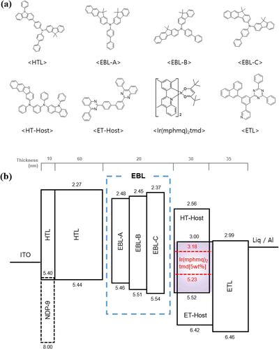
The materials and device structures referred to in this paper are shown in Figure . All devices were thermally deposited under a base pressure of 5 × 10⁻⁷ Torr in evaporation chambers without breaking the vacuum. The PhOLEDs employed indium tin oxide (ITO) as an anode; 2-(7-dicyanomethylene-1,3,4,5,6,8,9,10-octafluoro-7H-pyrene-2-ylidene)-malononitrile (NDP-9) doped N-([1,1′-biphenyl]-4-yl)-9,9-dimethyl-N-(4-(9-phenyl-9H-carbazol-3-yl)phenyl)-9H-fluoren-2-amine (BCFN) as a hole injection layer (HIL); BCFN as an HTL; N-([1,1′-biphenyl]-4-yl)-N-(9,9-dimethyl-9H-fluoren-2-yl)-11,11-dimethyl-11H-benzo[b]fluoren-2-amine (EBL-A), N-([1,1′-biphenyl]-4-yl)-N-(9,9-dimethyl-9H-fluoren-3-yl)-11,11-dimethyl-11H-benzo[b]fluoren-2-amine (EBL-B) and N-([1,1′-biphenyl]-4-yl)-N-(9,9-dimethyl-9H-fluoren-2-yl)-11,11-dimethyl-11H-benzo[b]fluoren-3-amine (EBL-C) as EBLs; Ir(mphmq)2tmd (bis(4-methyl-2-(3,5-dimethylphenyl)quinoline))Ir(III) (tetramethylheptadionate) as red phosphorescent dopants; N1-(naphtho[2,3-b]benzofuran-2-yl)-N1,N3-diphenyl-N3-(9-phenyl-9H-carbazol-2-yl)benzene-1,3-diamine as a hole transport type host (HT-Host); 2,2′-([1,1′-biphenyl]-3,4′-diyl)bis(4-phenylquinazoline) as an electron transport type host (ET-Host), 2-(3-(phenanthren-9-yl)-5-(pyridin-3-yl)phenyl)-4,6-diphenyl-1,3,5-triazine as an electron transporting layer (ETL); Liq (8-quinolinolato-lithium) as an electron injection layer; and Al as a cathode. After OLED fabrication, encapsulation was performed in a glove box using a glass lid, CaO getter, and epoxy adhesives to protect the device from oxygen and moisture. The whole device structure was ITO (120 nm)/HIL (10 nm)/HTL (60 nm)/EBL (20 nm)/EML (30 nm)/ETL (35 nm)/Liq (1.5 nm)/Al (200 nm). The EML comprised a mixed host with two hosts at a ratio of 50:50 and doped phosphor at a 5 wt% doping concentration. The hole-only device (HOD) structure without EML was ITO (120 nm)/HIL (10 nm)/EBL (100 nm)/Al (200 nm), and the HOD structure with EML was ITO (120 nm)/HIL (10 nm)/EBL (20 nm)/EML (30 nm)/HTL (30 nm)/Al (200 nm). The thin HIL (10 nm) layer in the HOD was used to form an Ohmic contact for hole injection to the active layers.
Figure 1. (a) Molecular structures of the materials used in organic light-emitting diodes (OLEDs) and (b) device structures based on EBLs’ A–C, showing the frontier orbital energy levels and thicknesses of the organic materials
2.2. Measurements
The current density(J)-voltage (V)-luminance and current efficiency-luminance-EQE characteristics of the devices were measured using a Keithley 2400 sourcemeter and a Konica Minolta CS2000 spectroradiometer. The lifetime test method was luminance measurement at constant current driving of the PhOLEDs at an initial luminance of 3000 cd m−2. The capacitance (C)-V analysis was performed with a Novocontrol Alpha-A. The amplitude of the alternating current (AC) voltage is 100 mV, and the AC voltage is superimposed on the direct current (DC) bias and measured at a frequency of 100 Hz. The transient electroluminescence (EL) decay of the OLEDs was obtained using a Keysight 33500B function generator, a Keysight DSOX3012T oscilloscope, a Hamamatsu H10721-110 photomultiplier, and a DHPCA-100 current amplifier. Finally, the device lifetime of the PhOLEDs was characterized using the McScience M6000 lifetime measurement system.
3. Results and discussions
The three EBLs have a common structure with the tri-aryl amine core moiety substituted by three aryl groups of biphenyl, dimethyl-9H-fluorene, and 11,11-dimethyl-11H-benzo[b]fluorene. Two aryl groups, dimethyl-9H-fluorene, and 11,11-dimethyl-11H-benzo[b]fluorene, were introduced at 2 and 2 positions in EBL-A, 3 and 2 positions in EBL-B, and 2 and 3 positions in EBL-C, respectively. The lone pair electrons in the N atom were delocalized on the aromatic ring, which allowed the EBLs to have hole transport properties and electron-blocking characteristics. In addition, the difference in substitution positions of the three EBLs may make differences in photophysical characteristics and device performances. The HOMO levels of the EBLs were −5.46, −5.51, and −5.54 eV for EBL-A, EBL-B, and EBL-C, respectively, by cyclic voltammetry. The HOMO levels of the hole transport host and the electron transport host were −5.52 and −6.42 eV, respectively, and the phosphorescent dopant was −5.23 eV, suggesting a significant HOMO gap (0.29 eV) for hole trapping between hole transport host and phosphor.
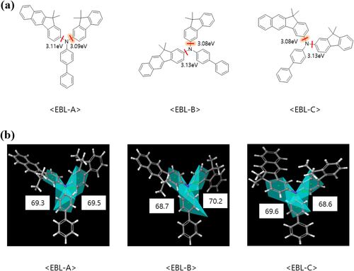
The bond dissociation energy (BDE) of each EBL was calculated using Gaussian software to understand the intrinsic stability of the EBLs. As depicted in Figure (a), the difference in BDE is not large, depending on the substituent position, indicating that they exhibit similar stability under electrical stress conditions. The difference in bond angles was also quite small, as revealed in Figure (b), suggesting that the dihedral angle did not affect the stability of the EBL.
Figure 2. (a) Bond dissociation energy for three EBL materials and (b) bond angle depending on the bond position for three EBL materials
HODs were fabricated to analyze each EBL’s difference in field-dependent mobility, stability, and hole injection behavior. First, the field-dependent mobility was extracted using impedance spectroscopy analysis methods [Citation22–32]. All devices showed clear peaks in the imaginary Z Spectra (Z″) according to frequency (f), and the mobility can be determined by the peak f [Citation22,Citation24,Citation31,Citation32]. The Z″-f spectra of all HODs are presented in Figure . The peak frequency is related to mobility by the following equation:
(1)
(1)
(2)
(2) Where
,
,
,
,
, and
are the peak frequency, numerical coefficient, average transit time, charge carrier mobility, thickness of the device, and DC voltage, respectively. The coefficient
was used as about 0.44, which was determined by an analytical simulation of the appropriate dispersion of hopping transport [Citation32].
Figure 3. DC voltage-dependent imaginary Z-frequency spectra of hole-only devices of (a) EBL-A, (b) EBL-B, and (c) ELB-C. The transit time of the charge carrier in the charge-only device is determined from the peak frequency of Z″-f spectra.
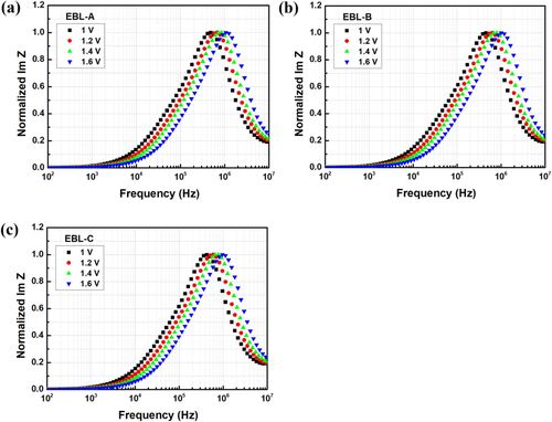
Figure presents the mobility and J-V characteristics of EBL materials. Specifically, Figure (a) demonstrates that the field-dependent mobility is similar. However, the J-V characteristics in Figure (b) indicate a similar J increase in devices without EML but a dissimilar J increase in devices with EML in the order of EBL-C > EBL-B > EBL-A. The overall decrease of current density in the HODs with EML is due to the formation of a hole injection barrier and poor hole transport properties of EML by the strong hole trap of phosphorescent dopant as can be expected from the energy level diagram in Figure . Considering the difference in the HOMO level of each EBL, EBL-C with a deep HOMO level has a high J at the same V due to efficient hole injection into EML, whereas the EBLs with a shallow HOMO level exhibit a low J because of the large energy barrier for hole injection from EBL to EML. The carriers were accumulated in the EBL or at the EBL/EML interface by the large injection barrier.
Figure 4. (a) Field-dependent hole mobilities of electron blocking layers (EBLs); (b) Current density versus voltage characteristics for the hole-only devices (HODs); With EML, the voltage rises significantly at the same current, and the trend differs from without EML; (c) Voltage rise of HODs in the stability test at a current density of 10 mA/cm2
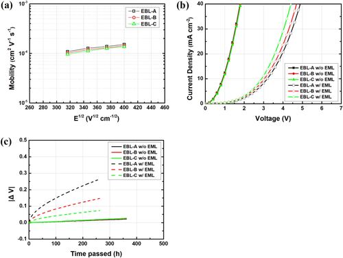
The hole accumulation in the devices by the shallow HOMO levels of EBL is expected to increase the resistance of the device and induce polaron-triggered deterioration processes. The stability test of the HOD with and without EML was conducted by stressing the HOD at a current density of 10 mA/cm2 to examine the effect of EBL on the stability of the devices. As detailed in Figure (c), the HODs without EML exhibit a similar voltage increase, but the HODs with EML confirm that different voltage levels increase depending on the EBL. A significant increase in the driving voltage is observed in the EBL-A device, while a small increase in driving voltage is noted in the EBL-C device. The increase in voltage means the deterioration of the material under positive polarons affects the device’s resistance change. The deterioration by polarons is reduced in the order of EBL-A, EBL-B, and EBL-C, which is well correlated with the hole injection behavior of the EBLs.
To analyze the electrical and luminescence characteristics of the three EBLs embedded devices, three PhOLEDs with different EBLs were fabricated. The J-V-luminance and current efficiency-luminance-EQE characteristics are shown in Figure , and the device performances are summarized in Table . As specified in Figure (a), the EBL-A device shows relatively high turn-on voltage at 1 cd/m2 and the driving voltage at 3000 cd/m2 compared to other devices because of poor hole injection into the EML, whereas the EBL-C device exhibits the lowest turn-on and driving voltages due to efficient hole injection into the EML.
Figure 5. (a) Current-density-voltage-luminance; (b) Parallel capacitance-voltage at an AC frequency of 100 Hz with voltage-luminance; (c) Current efficiency–luminance–external quantum efficiency (EQE); (d) Device lifetime at initial luminance of 3000 cd m−2. The capacitance is the result of the total contribution of charge accumulation at the interface, charge injection into EML, and recombination.
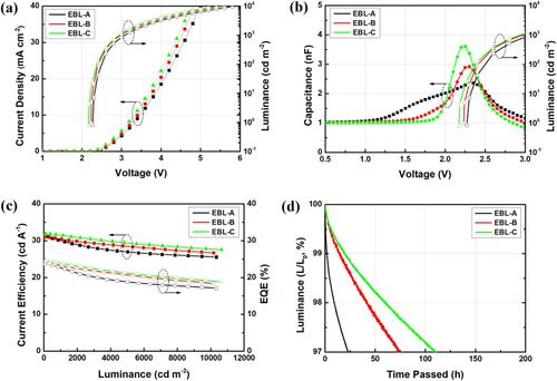
Table 1. Performances and lifetimes of devices.
The hole injection properties can be characterized by C-V analysis and the C-V-luminance characteristics of the PhOLEDs are presented in Figure (b). The C of the devices is generally caused by accumulated or trapped polarons inside the devices. Typically, the C of the devices is sharply increased near turn-on voltage by injected carriers and then quickly reduced by recombination of the carriers. Only the EBL-C device follows the trend of the conventional device and the other two devices display abnormally high C values even at the low voltage less than the turn-on voltage. This means that carriers were accumulated in the devices by inefficient carrier injection possibly due to a large energy barrier at the EBL/EML interface. In addition, the C of the EBL-C device was much higher than that of the other devices near turn-on voltage by high carrier density through efficient carrier injection.
The different carrier injection affects the device performances at low and high luminances. As shown in the current efficiency-luminance-EQE characteristics in Figure (c), the device with EBL-C exhibits higher EQE, higher current efficiency, and significantly lower roll-off (7.2% at 3000 cd m−2) than the devices with EBL-A and EBL-B (14.3%, 8.8% at 3000 cd m−2, respectively). Both efficiency and efficiency roll-off were improved in the device with EBL-C, and this can be explained by the change of charge balance and recombination zone (RZ). The EQE is generally determined by the following equation:
(3)
(3) where
represents the charge balance,
represents the radiative exciton ratio,
represents the PLQY of the emitting material, and
represents the outcoupling efficiency. In the three devices,
and
can be assumed to be the same because similar EBLs were used, and
can also be assumed to be similar because the refractive index of EBLs was similar (i.e. The refractive index of the EBLs are 1.77, 1.76, and 1.76 for EBL-A, EBL-B, and EBL-C, respectively). Therefore, the difference in EQE is mainly attributed to the charge balance (
), resulting in high EQE in the EBL-C device. In addition, the distance between excitons in the unit area becomes closer (increased exciton density) when the RZ becomes narrow, and the quenching between triplet excitons like triplet–triplet annihilation (TTA) is aggravated due to the long exciton lifetime of the triplet excitons [Citation33–37]. As the TTA is mainly responsible for the EQE roll-off and is closely related to RZ, the RZ of the devices with different EBLs was examined. To confirm the RZ in EML, six devices with different phosphor-doped EML thicknesses were prepared. The total thickness of EML is 30 nm, and the thickness of the doped EML and non-doped EML is managed, as shown in Figure . It can be expected that RZ is formed closer to EBL than ETL due to the strong hole trap of the phosphorescent dopant. In addition, since the electron trap by the dopant is relatively weak, changes in carrier balance by the dopant may not significantly affect the formation of RZ. The RZ monitoring devices are fabricated for the three EBLs. Figure displays the current efficiency–luminance characteristics according to the doped layer thickness, and Table lists the performance of all devices. Devices with a doped layer thickness of ∼8 nm from the EBL/EML interface exhibited a decreased efficiency with an increased roll-off compared to devices with a total doped layer thickness of ∼30 nm. The increased efficiency roll-off indicates that the quenching of triplet excitons by TTA is serious by narrow RZ. The current efficiency roll-off is not worsened when the doped layer thickness reaches ∼10 nm in the EBL-A device, proposing that the RZ of the EBL-A device is mostly confined within ∼10 nm from the EBL/EML interface. The RZ of the EBL-B and EBL-C devices is estimated to be confined within ∼11 nm and ∼12 nm from the EBL/EML interface, respectively, using the same RZ analysis method. The width of the RZ is in the order of EBL-C > EBL-B > EBL-A and is well correlated with the hole injection behavior of the EBL as described in HOD data. The EBL-A device with poor hole injection ability exhibited narrow RZ and large efficiency roll-off by serious TTA, while the EBL-C device with good hole injection capability into EML showed wide RZ and small efficiency roll-off by weakened TTA. The reduction in TTA due to the broad RZ also increased in the device's lifetime. Figure (d) shows that the EBL-C device has the longest lifetime, whereas the EBL-A device has the shortest lifetime due to the degradation through hot excitons in EML by narrow RZ. Additionally, less accumulated polarons contribute to the long device lifetime of the EBL-C device. The efficient hole injection in the EBL-C device positively affected the efficiency roll-off and device lifetime through widened RZ and accompanying TTA suppression.
Figure 6. Device structures for confirming the formation of recombination zone in EML. The devices were fabricated by changing the dopant thickness doped to EML for three types of EBL.
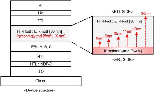
Figure 7. Current efficiency of the luminance of (a) EBL-A, (b) EBL-B, and (c) EBL-C devices. ∼30 nm is a doped device over the entire thickness of the EML.
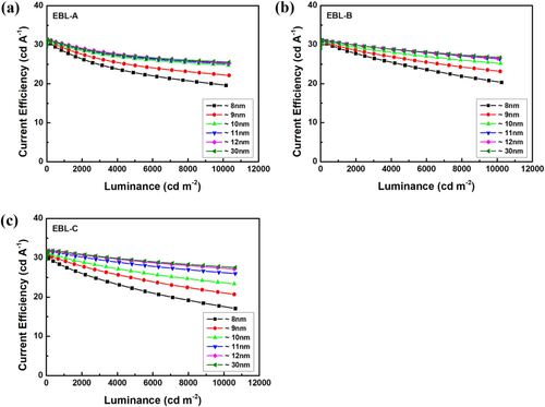
Table 2. Performances of devices
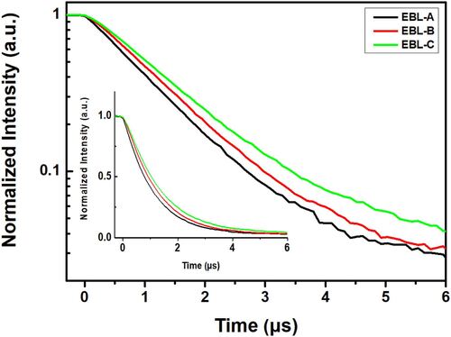
Finally, the decay time of the triplet exciton was also analyzed based on the result of the transient EL measurement. The length of the voltage pulse is 300 µs at a frequency of 2 kHz and the voltage pulse height corresponds to a current density of 15 mA cm−2. Since TTA affected by triplet exciton density can eventually be considered a quenching process, this may change the triplet exciton decay time [Citation38–41]. As shown in Figure , the transient EL decay time of the EBL-A device is shorter than that of the EBL-B device and that of the EBL-C device is relatively long compared to that of the other devices. As the TTA process quenches the triplet excitons of the phosphors, it accelerates the triplet exciton decay time of the devices. Therefore, it can be confirmed again that the TTA process is reduced in the EBL-C device.
Figure 8. Normalized intensity of the transient EL at the decay part. The length of the voltage pulse is 300 us and 2 kHz is periodically applied. The voltage pulse height corresponds to a current density of 15 mA cm−2 and was measured by turn-off at 0V.
4. Conclusions
In conclusion, three EBLs derived from triaryl amine were used to study the effects of the energy barrier between EBL and EML on the device performances of PhOLEDs. When the energy barrier was minimized, the hole injection characteristics were largely improved to form a wide RZ. TTA process could be minimized by forming a wide RZ, and the EQE was increased by more than 2% with a relaxed roll-off of 7% at 3000 cd/m2 and a device lifetime was increased fivefold. This work unveiled that the design of EBL can make a difference in the device performance of PhOLEDs.
Disclosure statement
No potential conflict of interest was reported by the author(s).
Additional information
Notes on contributors

Jinwoo Shin
Jinwoo Shin received his bachelor’s degree in 2015 from the Department of Information Display of Kyung Hee University in Seoul, Korea. Currently, he is a master’s degree candidate at the School of Chemical Engineering of Sungkyunkwan University in Suwon, Korea. In 2016, he joined Duksan Neolux in Cheonan, Korea, where he is a senior researcher in the research and development (R&D) Team. His major research area is the development of a novel device structure for organic electronic devices for high performance.

Jun Yeob Lee
Jun Yeob Lee received his Ph.D. degree from Seoul National University, Korea in 1998. After a postdoc at Rensselaer Polytechnic Institute (1998–1999), he joined Samsung SDI and developed an active matrix organic light emitting diode for 6 years. After that, he worked as a professor at the Department of Polymer Science and Engineering of Dankook University and he is now a professor at the School of Chemical Engineering of Sungkyunkwan University from 2015. His main research areas are the synthesis of organic electronic materials and the development of novel device structures for organic electronic devices.
References
- S. Scholz, C. Corten, K. Walzer, D. Kuckling, and K. Leo, Org. Electron. 8, 709 (2007).
- S. Scholz, K. Walzer, and K. Leo, Adv. Funct. Mater. 18, 2541–2547 (2008).
- V. Sivasubramaniam, F. Brodkorb, S. Hanning, H. Loebl, V. Elsbergen, H. Boerner, U. Scherf, and M. Kreyenschmidt, Cent. Eur. J. Chem. 7, 836 (2009).
- S. Scholz, R. Meerheim, B. Lüssem, and K. Leo, Appl. Phys. Lett. 94, 43314 (2009).
- I.R. de Moraes, S. Scholz, B. Lüssem, and K. Leo, Appl. Phys. Lett. 99, 53302 (2011).
- P.A. Lane, L.C. Palilis, D.F. O’Brien, C. Giebeler, A.J. Cadby, D.G. Lidzey, A.J. Campbell, W. Blau, and D.D.C. Bradley, Phys. Rev. B 63, 235206 (2001).
- A.J. Mäkinen, I.G. Hill, and Z.H. Kafafi, J. Appl. Phys. 92, 1598 (2002).
- X. Gong, J.C. Ostrowski, D. Moses, G.C. Bazan, and A.J. Heeger, Adv. Funct. Mater. 13, 439 (2003).
- A.J. Sandee, C.K. Williams, N.R. Evans, J.E. Davies, C.E. Boothby, A. Köhler, R.H. Friend, and A.B. Holmes, J. Am. Chem. Soc. 126, 7041 (2004).
- G. He, M. Pfeiffer, K. Leo, M. Hofmann, J. Birnstock, and R. Pudzich, J. Salbeck, Appl. Phys. Lett. 85, 3911 (2004).
- H. Yersin, Top. Curr. Chem. 241, 1 (2004).
- R. Liu, Z. Gan, R. Shinar, and J. Shinar, Phys. Rev. B 83, 245302 (2011).
- C. Weichsel, L. Burtone, S. Reineke, S. I. Hintschich, M. C. Gather, K. Leo, B. Lüssem, Phys. Rev. B 86 (2012) 075204.
- J.H. Lee, S. Lee, S.J. Yoo, K.H. Kim, and J.J. Kim, Adv. Funct. Mater. 24, 4681–4688 (2014).
- V.I. Adamovich, S.R. Cordero, P.I. Djurovich, A. Tamayo, M.E. Thompson, B.W. D’Andrade, and S.R. Forrest, Org. Electron. 4 (2-3), 77–87 (2003).
- S. Jang, S.H. Han, J.Y. Lee, and Y. Lee, Synth. Met. 239, 43–50 (2018).
- R. Meerheim, S. Scholz, S. Olthof, G. Schwartz, S. Reineke, K. Walzer, and K. Leo, J. Appl. Phys. 104, 014510 (2008).
- C.J. Huang, C.C. Kang, T.C. Lee, W.R. Chen, and T.H. Meen, J. Lumin. 129 (11), 1292–1297 (2009).
- J.A. Seo, S.K. Jeon, M.S. Gong, J.Y. Lee, C.H. Noh, and S.H. Kim, J. Mater. Chem. C 3 (18), 4640–4645 (2015).
- C.H. Gao, D.Y. Zhou, W. Gu, X.B. Shi, Z.K. Wang, and L.S. Liao, Org. Electron. 14 (4), 1177–1182 (2013).
- J.Y. Huang, M.T. Wang, G.Y. Chen, J.Y. Li, S.P. Chen, J.H. Lee, T.L. Chiu, and Y.R. Wu, J. Phys. D: Appl. Phys. 53, 345501 (2020).
- S.W. Tsang, S.K. So, and J.B. Xu, J. Appl. Phys. 99, 13706 (2006).
- M. Schmeits, J. Appl. Phys. 101, 84508 (2007).
- T. Okachi, T. Nagase, T. Kobayashi, and H. Naito, Jpn. J. Appl. Phys. 47, 8965 (2008).
- T. Okachi, T. Nagase, T. Kobayashi, and H. Naito, Thin Solid Films 517, 1331 (2008).
- S. Ishihara, T. Okachi, and H. Naito, Thin Solid Films 518, 452 (2009).
- S. Ishihara, H. Hase, T. Okachi, and H. Naito, J. Appl. Phys. 110, 36104 (2011).
- D.C. Tripathi, A.K. Tripathi, and Y.N. Mohapatra, Appl. Phys. Lett. 98, 33304 (2011).
- S. Ishihara, H. Hase, T. Okachi, and H. Naito, Thin Solid Films 554, 213 (2014).
- K. Takagi, S. Abe, T. Nagase, T. Kobayashi, and H. Naito, , J. Mater. Sci. Mater. Electron. 26, 4463 (2015).
- J.M. Montero, J. Bisquert, G. Garcia-Belmonte, H.J. Bolink, and E.M. Barea, Phys. Status Solidi 204, 2402 (2007).
- J.M. Kim and J.J. Kim, Org. Electron. 67, 43–49 (2019).
- M.A. Baldo, C. Adachi, and S.R. Forrest, Phys. Rev. B 62, 10967 (2000).
- N.C. Giebink, B.W. D’Andrade, M.S. Weaver, P.B. Mackenzie, J.J. Brown, M.E. Thompson, and S.R. Forrest, J. Appl. Phys. 103, 44509 (2008).
- C. Xiang, X. Fu, W. Wei, R. Liu, Y. Zhang, V. Balema, B. Nelson, and F. So, Adv. Funct. Mater. 26, 1463 (2016).
- Q. Wang, I.W.H. Oswald, M.R. Perez, H. Jia, B.E. Gnade, and M.A. Omary, Adv. Funct. Mater. 23, 5420 (2013).
- W. Song and J.Y. Lee, Adv. Opt. Mater. 5, 1600901 (2017).
- Y. Zhang, M. Whited, M.E. Thompson, and S.R. Forrest, Chem. Phys. Lett. 495, 161 (2010).
- D. Kasemann, R. Brückner, H. Fröb, and K. Leo, Phys. Rev. B 84, 115208 (2011).
- K. Masui, H. Nakanotani, and C. Adachi, Org. Electron. 14, 2721 (2013).
- J. Grüne, N. Bunzmann, M. Meinecke, V. Dyakonov, and A. Sperlich, J. Phys. Chem. C 124, 25667 (2020).