
 ?Mathematical formulae have been encoded as MathML and are displayed in this HTML version using MathJax in order to improve their display. Uncheck the box to turn MathJax off. This feature requires Javascript. Click on a formula to zoom.
Abstract
The subpixel size of high-resolution organic light-emitting diode (OLED) microdisplays measures a few micrometers. To achieve a full-color microdisplay, the current preference is to use photolithography technology on a white OLED instead of using a fine metal mask for patterning. The application of photolithography techniques allows for the creation of microcavity structures or color filters (CFs) to enhance color purity in each emitted color. This paper focuses on investigating specialized OLED device structures for high-resolution microdisplays. The characteristics of each structure, including efficiency and color gamut, are thoroughly discussed. The structure, combining microcavity and CF, achieves the widest color gamut, while microcavity structures show higher efficiency compared to CF-only structures. Tandem structures are also considered for improved efficiency and stability.
1. Introduction
In recent years, the term metaverse has become increasingly prevalent in information technology (IT). Creating a metaverse requires combining hardware capable of implementing augmented reality (AR) and virtual reality (VR) with a sense of liveliness, as well as software that offers diverse content to facilitate immersive experiences with others, even when physically separated. Among the essential hardware components for the metaverse, microdisplays have gained significant attention [Citation1]. While liquid crystal on silicon (LCoS) currently dominates the microdisplay market, many companies such as eMagin, Sony, BOE, and LG Display have also developed organic light-emitting diode (OLED) microdisplays [Citation2–5]. Compared to LCoS and digital micromirror device-based microdisplays, OLED microdisplays offer remarkable advantages, such as vivid image quality, fast response times, and a lightweight, compact form factor. As a result, commercial AR glasses and VR headsets utilizing OLED microdisplays have entered the market [Citation6].
While OLED microdisplay-based AR/VR products have been released, hardware developers continue to demand higher performance in terms of luminance, resolution, efficiency, and color gamut to enhance user satisfaction. Consideringthat AR/VR devices are designed to be portable and wearable, their battery capacity is limited to ensure a small and lightweight form factor. Consequently, high-efficiency displays are required to minimize battery consumption. Furthermore, a wide color gamut provides vibrant image quality and enables the same perceived quality as higher luminance, according to quality metrics [Citation7].
To achieve high efficiency and resolution in microdisplays, it is necessary to employ an OLED structure different from that used in conventional OLED displays. Large-sized OLED displays, led by LG Display, utilize a structure that applies color filters (CFs) to white OLEDs. On the other hand, small and medium-sized OLED displays, led by Samsung Display, adopt a structure that applies patterning technology for the light-emitting layer (EML) via a fine metal mask (FMM). While some companies such as eMagin and APS Research utilize FMM for full-color implementation, most OLED microdisplays announced so far apply CFs to white OLEDs. The white OLED structure in microdisplays differs from that of large-sized OLED displays. Microdisplays primarily employ single-stack OLEDs, while large-sized displays use 3-stack tandem OLEDs. Unlike conventional OLED displays driven by thin-film transistor circuits, OLED microdisplays driven by complementary metal–oxide semiconductor (CMOS) circuits are limited in their driving method. Additionally, as the gap between subpixels in high-resolution microdisplays becomes narrower, they are more susceptible to electrical leakage than conventional displays. Hence, this paper explores different structures utilizing CF, microcavity effects, and their combinations. Then, we review and propose OLED structure characteristics suitable for high-resolution microdisplays to achieve higher efficiency and a wider color gamut.
2. Experiments
The simulation of OLED devices with microcavity structures and varying thicknesses of the OLED structure was thoroughly described in the referenced paper [Citation8]. However, in the previous study, all phosphorescent materials were used in fabricating the devices. It was found that a blue phosphorescent dopant, bis2-(4,6-difluorophenyl) pyridinato-C2, Niridium(III) (FIrpic), did not achieve sufficient color purity. Therefore, in this study, a hybrid white OLED with a blue fluorescent material was employed [Citation9]. As the blue light-emitting material was changed, the blue cavity OLED’s thickness was adjusted accordingly. Furthermore, in the previous research, a second cavity structure was applied to the red cavity OLED to enhance color purity [Citation8]. However, due to the deeper photoluminescence (PL) of the blue emitter used in this study compared to the previous one, the first cavity structure was also employed in the red cavity OLED to prevent blue leakage. The detailed structure of the single white OLED is as follows: pHTL (10%, 10 nm)/HTL (depending on the cavity conditions)/blue EML (4 nm)/interlayer (4 nm)/green EML (2 nm)/red EML (4 nm)/ETL (30 nm)/LiF (1 nm)/Al (2 nm)/Ag (depending on device structures)/capping layer (60 nm). Here, HTL refers to the hole transport layer, and ETL stands for the electron transport layer. The thicknesses of HTL are 60, 130, 170, and 240 nm for the first red, second blue, second green, and second red cavities, respectively. In the white OLED designed for CF applications, an Ag thickness of 12 nm was used to reduce the microcavity effect, while 40 nm was applied in the structure to enhance the microcavity effect. The fundamental properties of the materials used and the hybrid white OLEDs’ device properties were elaborated in [Citation10]. The tandem white OLED’s structure is pHTL (10%, 10 nm)/HTL (depending on the cavity conditions)/blue EML (20 nm)/ETL (20 nm)/nETL (20 nm)/pHTL (10 nm)/HTL (30 nm)/green and red EML (20 nm)/ETL (40 nm)/LiF (1 nm)/Al (2 nm)/Ag (40 nm)/ capping layer (60 nm) [Citation11].
3. Results and discussion
3.1. OLED structure for high-resolution microdisplay
Figure classifies OLED structures based on the manufacturing technologies employed for OLED devices. Due to the small subpixel size of microdisplays, OLED microdisplays utilize Si substrates with CMOS circuits. The last metal layer of the CMOS circuits, such as Ti/Al/TiN, serves as the pixel electrode [Citation12]. On top of this surface, an additional layer for a microcavity structure can be formed using photolithography. Using a transparent conductive material such as indium tin oxide for the microcavity layer is preferred, as it is positioned between the two electrodes of the OLED device. After depositing common organic layers for charge injection and transport via an open mask, the EML can be horizontally formed for red, green, and blue emission using FMMs or vertically formed for white emission through the open mask. The common organic layers for opposite charge injection and transport are then deposited on the EML via the open mask, followed by the deposition of a semi-transparent electrode to complete the OLED device. Thin-film encapsulation is applied to protect the device from moisture and oxygen. The individual colors of the red, green, and blue subpixels in OLED devices with white emission are typically generated through CFs formed using photolithography.
Figure 1. OLED structures for high-resolution microdisplay according to OLED manufacturing technology.
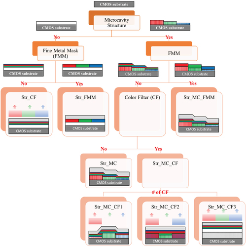
Based on the process technology, OLED devices can be classified into five structures: devices that only apply CF to white OLEDs (str_CF), devices that implement subpixels through FMM (str_FMM), devices that implement subpixels in white OLEDs through a microcavity structure (str_MC), devices that apply CF to OLEDs with a microcavity structure (str_MC_CF), and devices that simultaneously implement subpixels through FMM and a microcavity structure (str_MC_FMM). Figure summarizes OLED devices for high-resolution microdisplays. When applying CF to white OLEDs with a microcavity structure, it is unnecessary to use CFs for all subpixels. For example, the microcavity effect can be used to implement green and blue, while only red is implemented using CF (str_MC_CF1). Alternatively, only green can be implemented through the microcavity effect, while blue and red are implemented using CF (str_MC_CF2). Although a microcavity structure is applied, CFs may be used to further enhance color purity (str_MC_CF3). Ideally, each EML would be implemented using FMM. However, from a high-resolution standpoint, FMM still requires significant technological development. Therefore, this study focuses on structures that utilize technologies other than FMM.
3.2. Color gamut
Figure (a) presents the electroluminescent (EL) spectra of red, green, and blue emission in OLEDs with the str_CF structure. In this structure, the EL spectrum of each color is determined by the product of the white spectrum of the OLED and the transmittance of each CF. To expand the color gamut, the full width at half maximum (FWHM) of the CF needs to be narrowed since the FWHM of the photoluminescence (PL) of organic emitters is typically around 50 mm–100 nm. However, reducing the FWHM of the CF may also decrease its transmittance, resulting in reduced efficiency. Table summarizes the CIE color coordinates of red, green, and blue emissions in the str_CF structure and their color gamut based on the BT.2020 standard.
Figure 2. Electroluminescent spectrum of red, green, and blue emission in OLEDs with a structure of (a) str_CF, (b) str_MC, (c) str_MC_CF1, and (d) str_MC_CF.
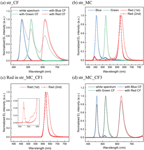
Table 1. CIE color coordinate and color gamut according to OLED structures.
Figure (b) shows that each emission can be achieved using only the microcavity effect without CF. The green emission in the blue EL can be adjusted based on the relative ratio of blue emission and green emission. Only green emission in the green cavity is observed without emission from other colors. In previous studies, the second red cavity structure showed only red emission due to the PL spectrum of a blue phosphorescent emitter not being deep enough [Citation8]. However, when hybrid white OLEDs using a blue fluorescent material are applied, some blue emission is observed due to the optical structure. The PL spectrum in the 450 nm–460 nm region may emit in the second red cavity structure, as indicated by the filled red triangle in Figure (b) [Citation8,Citation13], resulting in a very low x-coordinate of red emission compared to the BT.2020 standard.
The application of the first red cavity structure eliminates the blue emission but makes it difficult to block the green emission completely, which increases the x- and y-coordinates of red emission, which is unfavorable for color purity. Strictly speaking, by increasing the reflectance of the electrode through adjustments in the thickness of the thin metal layer or CPL, it becomes possible to reduce the FWHM of the emission spectrum , thereby blocking green emission. Nevertheless, such an excessively strong cavity effect is disadvantageous in terms of efficiency, primarily because the FWHM of the PL spectrum of the organic light-emitting materials remains relatively wide [Citation14,Citation15]. When CF is applied to the red subpixel (str_MC_CF1), blue or green leakage is eliminated, as depicted in Figure (c). The x-coordinate and the y-coordinate of red emission improve significantly, enhancing the color gamut. Table summarizes the CIE color coordinates of red emission in the str_MC and str_MC_CF1 structures and their color gamut based on BT.2020.
Although the cavity structure was applied, the color gamut based on BT.2020 still did not exceed 90. To further increase the color purity of each color, the str_MC_CF3 structure based on high-order cavity mode was fabricated. In this structure, a white OLED device was constructed that simultaneously satisfies the microcavity conditions for each color, and CFs were applied for each subpixel. By carefully adjusting the cavity length, multiple peaks at the resonance wavelength of red, green, and blue can be achieved [Citation8,Citation15]. The FWHM of the cavity gain spectrum is defined as:
(1)
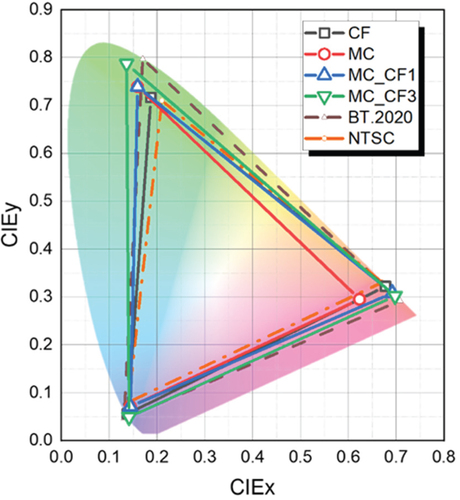
(1) where λ represents the peak emission wavelength, n stands for the refractive index, d is the cavity thickness, and Rt and Rb denote the reflectivity of the top and bottom contact, respectively [Citation16]. To achieve constructive interference, the cavity length is designed by multiples of λ/2. An increase in the cavity order implies an increase in the cavity thickness, reducing the FWHM of the EL spectrum. Consequently, the high-order cavity structure significantly decreases the FWHM of the EL spectrum for each color, thus enhancing color purity. In this structure, CF is responsible for distinguishing the spectra for each color. Although some green emission is observed in the blue subpixel because blue CF does not completely block the emission wavelength region above 500 nm, each color exhibits very high color purity, as demonstrated in Figure (d). Figure illustrates that the str_MC_CF3 structure covers a wider area in color space compared to str_MC_CF1, str_MC, and str_CF, and it achieves the widest color gamut based on BT.2020. Table summarizes the CIE color coordinates and color gamuts of OLEDs with the str_MC_CF3 structure. Consequently, in terms of color gamut, the stronger the microcavity structure applied, the more advantageous it is; hence, the application of CF to prevent the emission of other colors is beneficial.
Figure 3. CIE color coordinates of fabricated OLED devices.
3.3. Efficiency
Table details the current efficiency (CE) of OLEDs with the str_CF, str_MC, str_MC_CF1, and str_MC_CF3 structures. The CE may vary depending on the combination of red, green, and blue dopants in the EML of the hybrid single-white structure. However, the str_MC structure exhibits significantly higher efficiency in all colors compared to the str_CF structure. In the str_MC structure, each color’s efficiency is increased by utilizing a microcavity effect specifically designed for that color. The ideal CF would be 100% transparent for a specific color while completely blocking the rest. However, commonly used CFs, except for red, have a low transmittance of less than 80% [Citation11]. Therefore, in terms of efficiency, it is preferable not to use CF while applying the cavity effect.
Table 2. Current efficiency according to OLED structures at a current density of 5 mA/cm2.
As aforementioned, the red emission exhibits blue leakage in the second cavity structure or green leakage in the first cavity structure, and the use of red CF is necessary to improve the color gamut. Thus, if the color gamut issue is resolved by applying red CF, it is worth reconsidering whether to use the first or second red cavity structure in terms of efficiency. Table presents the CE of red cavity OLEDs based on cavity length and the presence (str_MC_CF1) or absence of CF (str_MC). The wide FWHM of the red dopant's PL spectrum reduces the efficiency as the cavity length increases [Citation17,Citation18]. Furthermore, as red emission is obtained from the white EML within the cavity structure, it may contain some other colors, which can affect current efficiency. Introducing red CF to eliminate leakage colors reduces the CE in both cavity structures, with a 35% reduction in CE for the first cavity structure and 25% for the second cavity structure, respectively. This reduction in efficiency stems from blocking other colors and CF transmittance of about 90%. As a result, when considering the characteristics of the cavity structure and CF, the CE is higher when CF is applied in the first structure than when CF is applied in the second structure.
The decrease in CE is less significant when red CF is applied than when green or blue CF is used. Each CF contains different types and concentrations of pigments, dyes, and dispersants, resulting in significant variations in their optical properties [Citation19,Citation20]. While it is possible to increase the transmittance of green and blue CF by reducing their thickness, this may increase the overlap between blue–green and green-red CF [Citation21,Citation22]. When utilizing OLED displays, preventing the emergence of other colors is crucial, even if the transmittance of green and blue CF is relatively low. Therefore, the thickness of these CFs was determined to minimize the overlap with other colors. In contrast, red CF typically maintains a transmittance of over 90%, with minimal leakage of other colors [Citation21,Citation22]. Thus, applying a red CF with relatively high transmittance can help minimize the reduction in efficiency attributed to CFs. Simultaneously, it effectively prevents the leakage of other colors, thereby contributing to an improved color gamut.
The efficiency is slightly lower than that of the str_CF structure in the str_MC_CF3 structure, where microcavity structure and CF are applied, The intensity of cavity gain remains consistent regardless of the cavity order. However, as mentioned previously, when the cavity order increases, the FWHM of the cavity gain decreases. Consequently, due to the broad FWHM of the PL of organic light-emitting materials, efficiency decreases in high-order cavities. If an emitter with a narrow FWHM of PL, such as quantum dots and perovskite, is employed in these structures, the decrease in efficiency can be compensated for [Citation15,Citation23].
3.4. Tandem structure
To improve the efficiency and stability of OLED devices, it is essential to apply a tandem structure instead of a single structure. In the case of OLED microdisplays driven by CMOS, there are limitations in the driving voltage range. However, it has been demonstrated that OLEDs with a two-stack tandem structure can be driven by CMOS [Citation24]. When using a hybrid white EML to achieve a wide color gamut, achieving high efficiency becomes challenging due to variations in the spectrum according to voltage, affecting the distribution of excitons in phosphorescent and fluorescent materials. However, these problems can be significantly alleviated by employing a two-stack tandem structure, substantially improving efficiency. The minimum thickness of organic layers required for a two-stack tandem structure restricts the application of the first cavity structure. Due to difficulties in obtaining a broad white spectrum in a tandem structure, the application of the str_CF structure is ineffective for achieving high efficiency. On the other hand, the str_MC_CF structure must be applied because red CF is essential in the second or higher cavity structure, as discussed previously in section 3.2.
Figure (a) displays the electroluminescent (EL) spectrum of red, green, and blue emission in tandem OLEDs with the str_MC_CF1 structure. Although some green leakage is still observed in the blue EL spectrum, it has been reduced compared to Figure (b). The green EL spectra are similar between single and tandem white OLEDs. There is the same blue leakage without CF in the red EL spectrum, but its removal through CF enables high color purity. Table summarizes the CIE color coordinates of blue, green, and red emissions in the tandem OLED with the str_MC_CF1. It achieves a color gamut of 85.7% based on the BT.2020 standard, similar to the single OLED with the same structure at 85.6%. To further increase the color gamut, a high-order cavity structure can be employed in tandem OLEDs.
Figure 4. Electroluminescent spectrum of red, green, and blue emission in tandem OLEDs with a structure of (a) str_MC_CF1 and (b) str_MC_CF3.
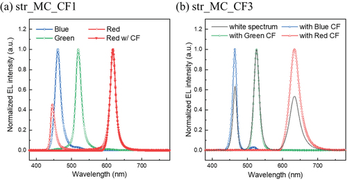
Table 3. CIE color coordinate, color gamut, and current efficiency of tandem OLEDs with a structure of str_MC_CF1 and str_MC_CF3.
Figure (b) specifies the EL spectrum of red, green, and blue emission in tandem OLEDs with the str_MC_CF3 structure. These EL spectra are similar to those in Figure (d) as the cavity structure predominantly determines the EL spectrum. The CIE color coordinates of red, green, and blue in tandem OLEDs with the str_MC_CF3 structure are listed in Table . The color gamut of the tandem OLEDs with the str_MC_CF3 structure is 97.9% based on the BT.2020 standard, like the single OLEDs with the same structure. However, there is a significant increase in CE in tandem OLEDs compared to single OLEDs. Table also summarizes the CE of blue, green, and red emission in tandem OLEDs with the str_MC_CF1 and str_MC_CF3 structures. In the str_MC_CF1 structure, the efficiency is increased by 8.6, 5.5, and 5.5 times for blue, green, and red, respectively, compared to single OLEDs with the same structure shown in Table . In the str_MC_CF3 structure, the efficiency is increased by 3, 10, and 7.4 times for blue, green, and red, respectively. This improvement in efficiency is primarily due to the difference in efficiency between single-white OLEDs and tandem-white OLEDs. While the CE of single white OLEDs is approximately 5 cd/A [Citation10], the CE of tandem white OLEDs is approximately 30 cd/A [Citation11]. Therefore, higher efficiency can be achieved while maintaining a wide color gamut by transitioning from a single-stack to a two-stack tandem OLED structure.
4. Conclusion
This paper has explored various OLED structures and technologies to improve the color gamut and efficiency of high-resolution microdisplays. The OLED structures were classified into five types based on their applicability in OLED fabrication. Among these structures, microcavity structures, CF, or a combination of both were analyzed. The results indicated that applying CFs to OLEDs with a microcavity structure can significantly improve color gamut. The combination of the strongest microcavity structure combined with CFs yields the largest color gamut. Efficiency is also addressed, showing that the microcavity structure generally leads to higher efficiency, while CFs may reduce it to some extent. Furthermore, by incorporating a 2-stack tandem structure in OLED devices with a microcavity structure, increasing efficiency while maintaining a wide color gamut becomes plausible. In conclusion, the study provides insights into OLED structures suitable for high-resolution microdisplays. The combination of microcavity structures, CFs, and tandem structures can potentially enhance color gamut and efficiency.
Acknowledgments
This work was supported by the Electronics and Telecommunications Research Institute (21ZB1200).
Disclosure statement
No potential conflict of interest was reported by the author(s).
Additional information
Notes on contributors

Hyunsu Cho
Hyunsu Cho received his B.S. and Ph.D. degrees in electrical engineering from Korea Advanced Institute of Science and Technology, Daejeon, Republic of Korea, in 2008 and 2014, respectively. He joined the Electronics and Telecommunications Research Institute, Daejeon, Republic of Korea, in 2014 and is currently a senior researcher. His research interests include device physics and optical design of optoelectronics devices, such as organic light-emitting diodes (OLEDs).

Chan-mo Kang
Chan-Mo Kang received his B.S. and Ph.D. electrical and computer engineering degrees from Seoul National University, Seoul, Republic of Korea, in 2008 and 2014, respectively. He is currently a senior researcher at the Electronics and Telecommunications Research Institute, Daejeon, Republic of Korea. His research interests include device engineering and physics in organic electronics, thin-film transistors, organic/inorganic hybrid devices, and high-resolution displays for augmented reality/virtual reality applications.

Sukyung Choi
Sukyung Choi received her B.S. degree from the Department of Nanomaterials Engineering at the Pusan National University, Pusan, Republic of Korea, in 2011, and her Ph.D. in Chemistry degree from Pohang University of Science and Technology, Pohang, Republic of Korea in 2016. She is currently a researcher at the Electronics and Telecommunications Research Institute, Daejeon, Republic of Korea. Her current research interests are optoelectronic devices with quantum dots (QDs), and organics such as LEDs and OLEDs.
Chul Woong Joo
Chul Woong Joo received his B.S. and M.S. degrees in polymer science and engineering of organic electronics devices from Dankook University, Yongin, Republic of Korea, in 2008 and 2010, respectively. He is currently a senior researcher at the Electronics and Telecommunications Research Institute (ETRI), Daejeon, Republic of Korea. He is currently interested in research on flexible display devices and microdisplays for augmented reality or virtual reality applications.

Byoung-Hwa Kwon
Byoung-Hwa Kwon received his B.S., M.S., and Ph.D. degrees from the Department of Materials Science & Engineering of Hanyang University, Pohang University of Science and Technology, and Korea Advanced Institute of Science and Technology, Republic of Korea, respectively, in 2006, 2008, and 2012. After graduating, he worked in the Department of Materials Science & Engineering of the University of Florida in Gainsville, USA, as a postdoctoral associate, and at LG Chem Ltd as a senior researcher. He joined the Electronics and Telecommunications Research Institute, Daejeon, Republic of Korea, in 2014. His current research interests are optoelectronic materials and devices, such as OLEDs, QD (quantum dot)-LEDs, photodetectors, and thin-film encapsulation for flexible devices.

Jin-Wook Shin
Jin-Wook Shin received his B.S. and M.S. degrees from Myongji University and Kwangwoon University, Republic of Korea, respectively. In 2018, he received his Ph.D. degree from Tohoku University, Japan. He joined the Electronics and Telecommunications Research Institute, Daejeon, Republic of Korea, in 2009. His current research interests include flexible display devices, microdisplays for augmented reality or virtual reality, and implantable biomedical devices.

Kukjoo Kim
Kukjoo Kim received his B.S. and Ph.D. in electrical engineering from the Korea Advanced Institute of Science and Technology in 2008 and 2014, respectively. He is currently working as a senior researcher at the Electronics and Telecommunications Research Institute. His research interests include the integration of displays and sensors for biomedical applications.
Dae Hyun Ahn
Dae Hyun Ahn received his B.S. and Ph.D. in display engineering from Kyung Hee University in 2015 and 2020, respectively. He joined the Electronics and Telecommunications Research Institute, Daejeon, Republic of Korea, in 2020 as a postdoctoral associate and is currently a senior researcher. His research interests include OLED materials, OLED device technology, and microdisplays for augmented reality or virtual reality applications.
Nam Sung Cho
Nam Sung Cho received his B.S. degree from Chung-Ang University, Seoul, South Korea in 2000, and his M.S. and Ph.D. Chemistry degrees from KAIST in 2002 and 2006, respectively. From 2006 to 2008, he was a postdoctoral associate at the University of California, Santa Barbara. He worked on materials development for OLEDs at LG Display R&D Center, Paju, from 2008 to 2011. He joined ETRI in 2011. His current research interests are focused on OLED structure, OLED materials, and white OLEDs.
References
- C.-M. Kang, and H. Lee, Recent progress of organic light-emitting diode microdisplays for augmented reality/virtual reality applications, J. Inf. Display 23 (1), 19–32 (2022).
- A. Ghosh, E.P. Donoghue, I. Khayrullin, T. Ali, I. Wacyk, K. Tice, F. Vazan, O. Prache, Q. Wang, L. Sziklas, D. Fellowes, and R. Draper, Ultra-high-brightness 2 K × 2 K full-color OLED microdisplay using direct patterning of OLED emitters, SID Symp, Dig, Tech. Pap 48 (1), 226–229 (2017).
- T. Fujii, C. Kon, Y. Motoyama, K. Shimizu, T. Shimayama, T. Yamazaki, T. Kato, S. Sakai, K. Hashikaki, K. Tanaka, and Y. Nakano, 4032 ppi high-resolution OLED microdisplay, J. Soc. Inf. Display 26, 178–186 (2018).
- P. Lu, G. Huang, S. Yang, X. Chen, X. Dong, H. Wang, Y. Wang, M. Xuan, C. Zhang, M. Yang, C. Wang, and H. Yue, Highest ppi micro-OLED display sustain for near-eye application, SID Symp, Dig. Tech. Pap 50, 725–726 (2019).
- C. Vieri, G. Lee, N. Balram, S.H. Jung, J.Y. Yang, S.Y. Yoon, and I.B. Kang, An 18 Megapixel 4.3’’ 1443 ppi 120 Hz OLED display for wide field of view high acuity head mounted displays, SID Symp, Dig. Tech. Pap 49, 5–8, (2018).
- S. Lee, Y. Chen, J. Kim, and J. Jang, Vertically integrated, double stack oxide TFT layers for high-resolution AMOLED backplane, J. Soc. Inf. Display 28, 469–475 (2020).
- R. Zhu, H. Luo, Y. Chen, and S.-T. Dong, Wu, Realizing Rec. 2020 color gamut with quantum dot displays, Opt. Express 23 (18), 23680–23693 (2015).
- H. Cho, C.W. Joo, S. Choi, C.-M. Kang, B.-H. Kwon, J.-W. Shin, K. Kim, D.H. Ahn, and N.S. Cho, Organic light-emitting diode structure for high color gamut in high-resolution microdisplay: Over 90% color gamut based on BT.2020, Org. Electron 101, 106419 (2022).
- J. Park, J.-H. Lee, J. Lee, and H. Cho, Effect of a P-doped hole transport and charge generation layer on single and two-tandem blue top-emitting organic light-emitting diodes, J. Inf. Display 22 (2), 107–113 (2021).
- S.J. Lee, C.-M. Kang, J.-W. Shin, D.H. Ahn, C.W. Joo, H. Cho, N.S. Cho, H.M. Youn, Y.J. An, J.S. Kim, J. Lee, and H. Lee, Three-wavelength white organic light-emitting diodes on silicon for high luminance and color gamut microdisplays, J. Ind. Eng. Chem 105, 132–137 (2022).
- H. Cho, C.W. Joo, S. Choi, C.-M. Kang, G.H. Kim, J.-W. Shin, B.-H. Kwon, H. Lee, C.-W. Byun, and N.S. Cho, Design of white tandem organic light-emitting diodes for full-color microdisplay with high current efficiency and high color gamut, ETRI J 43 (6), 1093–1102 (2021).
- H. Lee, H. Cho, C.-W. Byun, C.-M. Kang, J.-H. Han, J.-I. Lee, H. Kim, J.H. Lee, M. Kim, and N.S. Cho, Device characteristics of top-emitting organic light-emitting diodes depending on anode materials for CMOS-based OLED microdisplays, IEEE Photonic. J 10 (6), 8201809 (2018).
- H. Cho, C.W. Joo, B.-H. Kwon, C.-M. Kang, S. Choi, and J.W. Sin, Correlation between optimized thicknesses of capping layer and thin metal electrode for efficient top-emitting blue organic light-emitting diodes, ETRI J. doi:10.4218/etrij.2022-0236.
- S. Hofmann, M. Thomschke, P. Freitag, M. Furno, B. Lüssem, and K. Leo, Top-emitting organic light-emitting diodes: Influence of cavity design, Appl. Phys. Lett 97, 253308 (2010).
- J.Y. Kim, S.Y. Lee, K.H. Cho, and Y.S. Do, Dual-microcavity technology for red, green, and blue electroluminescent devices, Adv. Funct. Mater. 2305528 (2023), doi:10.1002/adfm.202305528.
- S. Hofmann, M. Thomschke, B. Lüssem, and K. Leo, Top-emitting organic light-emitting diodes, Opt Express 19, A1250–A1264 (2011).
- J.-X. Man, S.-J. He, C.-S. Shi, H.-N. Yang, D.-K. Wang, and Z.-H. Lu, Optical design of connecting electrodes for tandem organic light-emitting diodes, Opt Lett 45, 3561–3564 (2020).
- M.J. Park, Y.H. Son, G.H. Kim, R. Lampande, H.W. Bae, R. Pode, Y.K. Lee, W.J. Song, and J.H. Kwon, Device performances of third order micro-cavity green top-emitting organic light emitting diodes, Org, Electron 26, 458–463 (2015).
- J. Choi, S.H. Kim, W. Lee, C. Yoon, and J.P. Kim, Synthesis and characterization of thermally stable dyes with improved optical properties for dye-based LCD color filters, New J Chem 36, 812–818 (2012).
- J.W. Namgoong, S.H. Kim, S.-W. Chung, Y.H. Kim, M.S. Kwak, and J.P. Kim, Aryloxy- and chloro-substituted zinc(II) phthalocyanine dyes: Synthesis, characterization, and application for reducing the thickness of color filters, Dyes and Pigments 154, 128–136 (2018).
- Z. Luo, S. Xu, Y. Chen, Y. Liu, and S.-T. Wu, Prospects of quantum dots-based liquid crystal displays, Proc, SPIE 9005, Advances in Display Technologies IV 90050G (2014).
- J. He, H. Chen, H. Chen, Y. Wang, S.-T. Wu, and Y. Dong, Hybrid downconverters with green perovskite-polymer composite films for wide color gamut displays, Opt Express 25, 12915–12925 (2017).
- H. Cho, C.-M. Kang, B.-H. Kwon, S. Choi, C.W. Joo, and H. Lee, Luminance compensation in top-emitting organic light-emitting diodes with high color purity as quantum dots using horizontal dipole orientation, Org. Electron 87, 105945 (2020).
- H. Cho, C.-W. Byun, C.-M. Kang, J.-W. Shin, B.-H. Kwon, S. Choi, N.S. Cho, J.-I. Lee, H. Kim, J. Hwan Lee, M. Kim, and H. Lee, White organic light-emitting diode (OLED) microdisplay with a tandem structure, J. Inf. Display 20 (4), 249–255 (2019).