
 ?Mathematical formulae have been encoded as MathML and are displayed in this HTML version using MathJax in order to improve their display. Uncheck the box to turn MathJax off. This feature requires Javascript. Click on a formula to zoom.
Abstract
Thin Se films with an appropriate thickness were deposited by the thermal evaporation technique on glass substrates that are grasped at a temperature of ∼300 K. The as-deposited amorphous Se thin films were heat-treated in N2 ambient for 1 h at different annealing temperatures that ranged from 323 to 363 K. The transmittance spectra of green and annealed Se films have been measured at vertical incidence angle along the wavelength range of 300–2500 nm. For the first time, the dielectric function (OJL2) model modified by O’Leary, Johnson, Lim was used alone to fit very well the transmission spectra along the whole wavelength range and extract the optical parameters of Se films. For each value of photon energy, the value of the complex dielectric function of all examined Se films was obtained. By simulating, the model parameters (absorption coefficient α, real and imaginary dielectric constants, refractive index n and optical bandgap Eg) and the film thickness have been deduced. We found that the index of refraction increased by increasing the annealing temperatures. Optical bandgap energy of Se films changes slowly from 2.0 eV of virgin a-Se film to 1.6 eV as the annealing temperature was raised to 343 K and then increased again from 1.93 eV to 2.2 eV for films annealed at temperatures that ranged from 348 to 363 K. By heat treatment crystallization of a-Se films occurred at and above the annealing temperature of 348 K that was confirmed by XRD patterns. The amorphous film showed a smooth surface consisting of very small grains of 40 nm size and low roughness of 1.9 nm. The grain size decreases, while roughness increased by increasing the annealing temperatures.
1. Introduction
Serious attention and great efforts are paid for studying the chalcogenide glasses that are defined as compounds composed of at least one element from the sixth group of the Periodic Table (S, Se or Te), due to their significant applications in modern technology. Among several compositions and alloys of chalcogens, the modest form is the pure elements, selenium for example. Pure selenium films and its alloys create a centre of consideration due to its numerous applications such as memory appliances, electrophotography and switching [Citation1–7]. Nowadays, Se film is used as a photoconductor in HARPICON camera for high-sensitivity TV, x-ray sensitive vidicons (X-icon), electro-photographic (Xerography) and IR fibre optics and as a Videocon photoconductor material [Citation8–11].
Besides its amorphous state, selenium has three major structures: trigonal and two monoclinic phases [Citation12,Citation13]. In the trigonal (hexagonal) phase, selenium is made of helical Sen chains, while in α- and β-monoclinic phases, selenium involves Se8 rings. For both trigonal and monoclinic phases, a covalent bond is the predominant force between Se atoms, while the chains or rings are bonded together by the Van der Waals force. The hexagonal structure phase exhibits high electrical conductivity and more stability. By using heat treatment, the relatively high resistive structure can be converted into the hexagonal structure. The values of bandgap energy range between 1.7 and 2.2 eV for the trigonal selenium phase and 2.4–2.6 eV for the monoclinic phase [Citation14]. Based on the preparation method, chains and rings are mixed with different ratios to form the amorphous selenium phase [Citation15].
For fabricating and designing the semiconductors-based optoelectronic devices, the optical constants of the semiconductor materials should be determined accurately. Despite considerable efforts have been devoted to studying the optical characteristics of thin Se films, its optical constants and behaviour are still less than adequate. Several mathematical models have been developed for characterizing the transmittance and/or reflectance spectra of different optical materials [Citation16–23]. Generally, the optical behaviour of thin films can be predicted by finding out the values of refractive index and dielectric function over a certain wavelength range. The complex dielectric function ε and complex refractive index ñ are related by , thus
, where εi is the imaginary part and εr is the real part of the dielectric function, n is the refractive index and k is the extinction coefficient. Several dielectric function models [Citation24–28] are useful for concluding the dielectric constant and refractive index of thin films by fitting the optical transmittance and/or reflectance data. For microcrystalline silicon (µc-Si:H) thin films, the optical constants have been evaluated by fitting T and R spectra using OJL2 model [Citation29]. Also, the spectroscopic ellipsometry data of thick a-Se film have been analysed by applying Jellison–Modine model [Citation30], and the optical constants have been calculated [Citation31].
Previously, we have published an article [Citation32] describing the optical parameters of the a-Se film which comprise the dielectric functions (ε = εr + iεi), complex refractive index, N = n + ik where, and the optical band gap (Eg) was determined. We have used OJL model to describe the dielectric function of the as-deposited a-Se films by fitting the transmission spectrum only. This paper deals with studying the role of annealing temperature on the optical characteristics of thin Se films. The dispersion OJL model of the optical constants is used to find out the thermally induced variation of the optical parameters of Se films. For the first time, to the best of our knowledge, the optical coefficients of Se films annealed at various temperatures will be calculated and correlated with their morphology and microstructure.
2. Materials and methods
Proper volumes of pure Se powder of 99.99% purity (Sigma Aldrich Co.) were evaporated on microscopic slide substrates by using the thermal evaporation chamber at room temperature. Prior to the deposition process, the microscopic slides of 1.1 mm thickness were cleaned carefully by immersion in acetone under ultrasonic vibration, then moved to ethanol solution for 0.5 h, and then washed by deionized water. Inside the coating unit, a high current (100A) is used for heating a tungsten boat containing the desired amount of Se that is evaporated to deposit on glass substrates held under vacuum with the pressure of 7.5 × 10⁻⁶ Torr. During the fabrication process, the glass substrates were mechanically rotating in order to get homogeneous Se films with uniform thickness. By this method, thin Se films having a thickness of around 1000 nm were obtained. The mechanical stylus profilometer (Veeco Dektak 150 surface profiler) was used to measure film thickness. The prepared Se films were subject to heat treatment by annealing at different temperatures (323–363 K). The structure of green and annealed Se films was inspected by recording the diffraction patterns of CuKα-radiation (λ = 1.5418 Å) used in X-ray diffractometer (Shimadzu XRD-6000). The surface morphology of the films was detected by using Atomic Force Microscope (AFM) (Veeco CP-II) in contact mode, while SEM (Shimadzu Superscan SSX-550) was used for observing the microstructure of the films. Shimadzu 3150 UV-VIS-NIR spectrophotometer of double-beam with 0.1 nm resolution was employed to measure the optical transmission spectrum, T(λ), of all films along wavelength range of (200–2500 nm) at the right angle of incidence.
The recognized software program (Scout) is used to get appropriate fitting of the transmittance spectra by applying the well-known dielectric function model, OJL2 model. Firstly, the formula of the OJL2 model was chosen and the basic value of the complex refractive index was inserted. The starting values of the film thickness and the model parameters were introduced. Running the program by applying the downhill simplex method by fluctuating the fit parameters (model parameters and film thickness) until an optimal fit is obtained. Finally, the film thickness, the dielectric function, the complex refractive index, and model parameters are printed. The deviation of the simulated data from the measured spectrum is calculated. More details about the dielectric function models and the fitting process are given in our previous work [Citation32].
3. Results and discussion
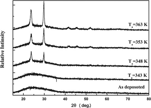
The amorphicity and crystallinity of as-deposited and annealed Se films are inspected by X-ray diffraction patterns shown in Figure . There are no peaks detected in the diffraction patterns of the as-prepared and annealed below 348 K films, indicating its amorphous state. The two sharp diffraction peaks (100) and (101) are presented in the XRD paradigms of the Se films after annealing at and above 348 K at 2θ = 23.75°and 29.77°, respectively, which correspond to the hexagonal phase structure reported in JCPDS 06-0362.
Figure 1. XRD diffraction patterns of the as-deposited and annealed at different temperature Se thin films.
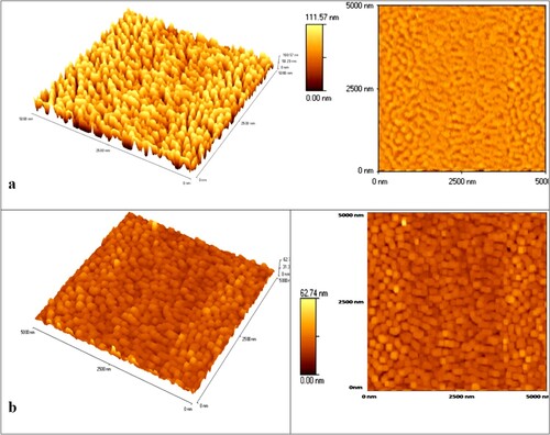
The morphological features of the virgin and annealed films were observed with an AFM. Three- and two-dimensional views of the amorphous and crystalline Se films are presented in Figure (a and b). Figure (a) shows a maze-like morphology of the as-deposited (a-Se) film consisting of wrinkle grains of about 55 nm size and high roughness of ∼15 nm. The crystallized Se film annealed at 363 K shows smoother surface composed of interconnected square or rectangular grain of around 25 nm size and low roughness of ∼9.5 nm. It is noticed that the grains are clearly visible and separated. Increasing the annealing temperatures decreases the size of grains and roughness of the film surface. As reported for several chalcogenide glasses [Citation33], increasing the surface roughness might be attributed to grain growth. Compared to those of the amorphous film, the individual grains of the crystalline film are connected to each other.
Figure 2. 3D (left) and 2D (right) AFM images of the surface topography for the as-deposited Se thin film (a) and Se film annealed at 363 K (b).
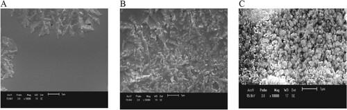
The SEM micrograph of unannealed Se film exhibits a high surface smoothness with no special features, not shown here. After the annealing at different temperatures, the surface morphology changes rapidly (Figure ), and the polycrystalline nature of the film becomes evident in the microphotograph. At the initial crystallization phase, the nucleation sites are considered as seeds for radial growth of spherical semi-crystalline regions (called spherulites) inside an amorphous medium. Spherulites are composed of very well-arranged lamellae linked by amorphous regions. The spherulites grow up to 60 μm in diameter and intermittently branch keeping a space-filling character. Figure (a) shows the formation of heterogeneous spherulites surrounded by glassy medium for film annealed at 348 K. This discontinuity is due to the presence of both crystallized region and amorphous matrix. This corresponds to the appearance of crystallization peak in XRD patterns (Figure ) at the beginning of the crystallization process. The growth of such spherulites is observed at the beginning of the crystallization process in amorphous Sb2S3 films [Citation33]. Increasing the annealing temperature increases the volume of crystallized regions, as shown in Figure (b), for film annealed at 353 K. Those intermediate and metastable crystallized regions are usually recrystallized by annealing at 363 K into fine-grained polycrystalline morphology with random orientation, as illustrated in Figure (c).
Figure 3. SEM micrographs of the as-deposited (A), annealed at 348 K (B) and annealed at 363 K (C) thin Se films.
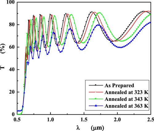
The optical transmission spectra T(λ) along the spectral wavelength ranged from 200 to 2500 nm of the green and annealed Se films are represented in Figure . For exhibiting the effect of annealing temperatures, T (λ) of some annealed films as an example is shown. All films show a high transparent window in the visible light range with strident absorption brink onset between 620 and 650 nm. According to their transmittance values, the transmission spectrum of all films can be classified into two regions namely: the transparent window, where T (λ) is around 70% and the strong absorption border, where T (λ) falls down to 0%. Such features have been observed for typical Se films [Citation34–36]. Also, it can be observed that the transmittance data of all samples exhibit interference effects, where a set of minima and maxima is observed in the wavelength range of high transmittance that is found at photon energies lower than that of the fundamental absorption edge. The oscillated values of the transmittance appear because of the interference resulted by the top film surface reflection in addition to the film and substrate interface. This interference fringe indicates the surface flatness and thickness uniformity of the films [Citation15]. On the other hand, it is clear that the optical transmittance decreased because of increasing the annealing temperature. The lowest value of transmittance was observed for films annealed at the temperature of 363 K.
Figure 4. Transmission spectra of the as-deposited and annealed at different temperatures of Se thin films.
Several models were used for simulating the transmission data where the fitting process was carried out in the profitable software SCOUT program [Citation37]. The best-fitting was obtained by applying the OJL model. Firstly, we have applied some of Kim’s oscillator models and found out the dielectric parameters of the glass substrate slides [Citation31]. By getting a very high correspondence between the experimentally measured and simulated transmittance spectra, the acquired values of dielectric constants of glass slides were inserted as a database in the used software program Scout 2. Secondly, we insert the transmission data of Se thin film and applied OJL2 model through the configuration of Se film/glass substrate in order to simulate transmission spectra that fit very well with the measured one. By using OJL2 model only, transmittance spectra were fitted very well for all Se films. Figure shows the experimental and theoretical spectra of some films. It is clear that the positions and amplitude of the interference are very well fitted as well as the bandgap value and the absorption edge curvature. The best results were obtained by considering the film thickness and the model parameters as free fit parameters and using the downhill simplex method. The values of all free parameters, high-frequency dielectric constant ε∞ and optical gap energy Eg and are recorded in Table . As shown in Table , the obtained values of film thicknesses are in good agreement with those measured experimentally. This harmonization between the measured and simulated values of the film thickness indicates that OJL2 model is quite adequate for describing the optical properties of Se films.
Figure 5. Measured and fitted transmittance spectra of some Se films annealed at different temperatures.
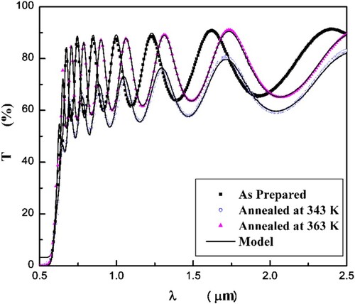
Table 1. The values of the OJL model parameters, optical band gap, deviation, measured and fitted film thickness of Se films at different annealing temperatures.
The relative percentage value of the difference between the measured points, Tiexp (λ), and the calculated transmission Tcalc (λ)
was obtained, and its value was found to be varied from less than 2% to around 7% in the high transparency and strong absorption regions, respectively. Moreover, as listed in Table , the minimum nonconformity value of 0.65–1.5 between simulated and experimental data was found. The low values of relative percentage errors and deviation confirm the suitability of OJL2 dielectric function model.
According to the OJL2 model, the imaginary part of the dielectric constant was calculated by using the joint density of states (JDOS), , that is a resultant from DOS;
(2)
(2) besides that, the absorption coefficient is derived by
(3)
(3) where
is the atomic density of the material and
is defined as the standardized dipole matrix component (called the oscillator strength). However, applying this equation demands that increasing the energy should increase the imaginary part of the dielectric function to infinity. Therefore, at high frequencies, the imaginary portion could be slowed down to zero by adding the so-called Decay factor by multiplying the following expression by
.
By applying the Kramers–Kronig dispersion equation, the real εr (ω) and the imaginary εi (ω) components of the dielectric function are related by.
(4)
(4) where ω is the frequency of interest, ω′ is the integration variable, and P is the Cauchy principal integral value, which is introduced for avoiding the singularity at ω = ω′.
Figure exhibits the spectral dependence of real and imaginary portions of dielectric function spectra resulted by applying the OJL2 model. On the right side, the εi (E) spectra of Se films are displayed. (1) part A shows εi (E) curves for amorphous Se films (curves of as-prepared, annealed at 333 K and annealed at 338 K Se films), (2) part B for mixed phases films (curves of Se films annealed at 343, 348 and 353 K) and (3) part C for crystalline films (curves for Se films annealed at 358 and 363 K). For amorphous Se films, part A, εi (E) spectra showed wide-highest structures in good agreement with the results reported by Innami et al. [Citation31] for a thermally evaporated a-Se film on Si substrate. The wider peak indicates the clean surface and the samples/ambient dielectric discontinuity. Moreover, it points to the high correct prediction of the dielectric function curve that is near to the curve of the bulk glass. This is in good agreement with the famous and simple principle “biggest is the best,” [Citation38] which is valid for amorphous and crystalline semiconductors. Decreasing the film roughness by annealing reduces the peak width and shifts the peak position to higher photon energy, as clear in curves of part C. The double peak appeared in part B might be attributed to the existence of both crystalline and glassy amorphous phases.
Figure 6. The real and imaginary parts of the dielectric functions of as-deposited and annealed at different temperatures of Se thin films.
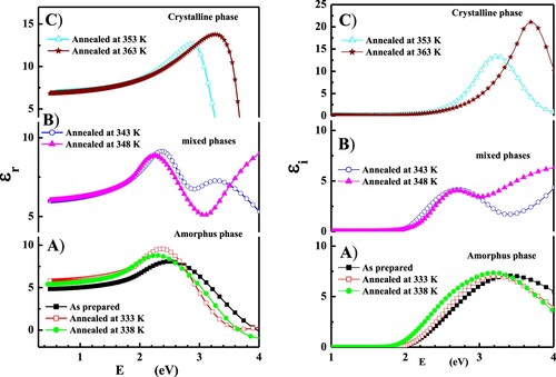
The left side on Figure demonstrates the spectral dependence of εr (E) of Se films. The green and annealed below 343 K Se films show the peak of εr (E) appears at around 2.5 eV. Such εr (E) peak has been observed for amorphous Se films by Innami et al [Citation31] and by Nagels et al. [Citation39] around 2.2 eV. For films annealed at 343 and 348 K, εr (E) spectra show two narrower peaks that might be attributed to the coexistence of amorphous and crystalline Se phases, that is confirmed by XRD patterns and SEM images. The first peak was at around 2.3 eV, and the second one was at 3.4 eV. The second peak was shifted to 4.0 eV by raising the temperature of annealing from 343 to 348 K. By increasing the annealing temperature up to 353 and 363 K, the first peak is disappeared and the second peak was shifted to lower photon energy (∼3.0 and 3.4 3 V, respectively).
There is another form of Kramers–Kronig-Relation (KKR), which gives a relation between refractive index n (ω) and extinction coefficient k (ω) by the following equations:
(5)
(5) and
(6)
(6) where k is obtained from its relationship to the absorption coefficient
Figure (a) displays the values of refractive index n computed at each value of wavelength. Obviously, the value of the refractive index slowly diminishes with increasing the wavelength, while its value increases with raising the heating temperature. It was found that at longer wavelengths, (frequency ≅ zero), n increases from 2.28 for virgin Se film to 2.42 for Se film annealed at 363 K. A notable excess in the values of refractive index was recognized as the temperature reached 348 K. This could be imputed to the transformation from the amorphous state to the crystalline state, as clear from the XRD patterns (Figure ). On the other hand, when the value of packing density is growing the film possesses the bulk value of refractive index [Citation40]
Figure 7. The real part of the refractive index (A) and extinction coefficient (B) of as-deposited and annealed at different temperatures of Se thin films.
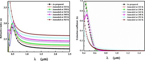
As mentioned above, the grains connected to each other by the thermal treatment resulting in more compact film and high packing density. Therefore, increasing the refractive index with temperature may be correlated to the packing density of the coating. Figure (b) shows the spectral distribution of the imaginary component of refractive index, extinction coefficient (k).
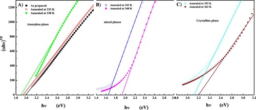
By using the OJL model parameters and Kramers–Kronig equations, the transmission spectrum could be used to gather absorption coefficient (α) of Se films. In the vicinity of the fundamental absorption edge, i.e. where α ≥ 104 cm−1, the optical absorption coefficient was described by the following relationship: , where
is the most important optical constant called the optical band gap energy [Citation41]. The optical band gap values
of green and annealed Se films were estimated from the linear part of
versus
graph, as plotted in Figure . The deduced fit parameter of the OJL2 model
and the obtained values of the bandgap energy
are scheduled in Table . The values of
and
are close to each other, especially for films annealed at high temperatures (≥348 K). Furthermore, some correlation between
and mass parameter (OJL2 model parameter) is observed. For higher
values, the mass parameter has higher values. A similar relationship between the mass parameter and
was described by Grdijn et al. [Citation29] when they studied the properties of µc-Si:H films.
Figure 8. (αhν)2 vs. photon energy hν for Se films annealed at different temperatures.
The bandgap energy varies by variation of the band tail states spreading around and
(the conduction and valance band edges, respectively). Increasing the spread of tail states gives rise to lessening the bandgap energy to lower than
. Meanwhile, narrowing spread or absence of band tail state resulted in a high amount of the bandgap energy. O’Leary had found the same conclusion when He extracted the optical bandgap value of GaAs and a-Si:H [Citation25,Citation42]. For our Se films, the optical band gap energy values decreased firstly from 2.0 eV for the as-deposited film to 1.65 eV when the film was annealed at 343 K, Figure (a,b) and then increased again from 1.92 eV to 2.2 eV, Figure (b,c), after raising the heat temperature from 348 to 363 K, respectively. This indicates that the narrow tail state spread and consequently large value of the optical band gap are the direct results of heat treatment.
As a final point, the classical single-oscillator dispersion model proposed by Wemple-DiDomenico (WDD) [Citation43] was used to investigate the obtained refractive index behaviour by using
(7)
(7) to find out the energies of single-oscillator
and of dispersion
, respectively. By fitting the linear part of
versus
graph for all samples, Figure , the values of
and
were calculated after extracting the slope,
and the intercept,
and.
Figure 9. 1/n2–1 vs. E−2 of Se films, the static refractive index n (0) at E2 = 0.
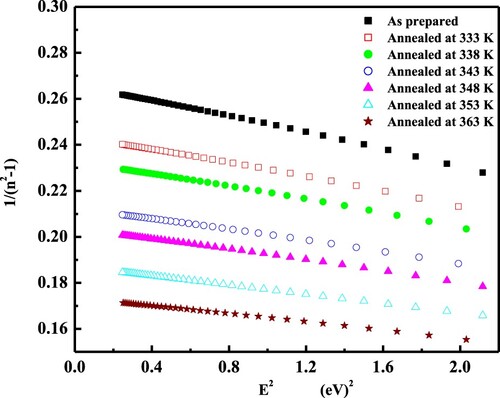
In Table , we summarized the values of all optical parameters (,
and
). To a good approximation, the value of
is varied in directly proportional to the optical bandgap energy
;
∼(1.5–2)
[Citation44]. On the other hand,
also increased by raising the temperature of annealing. In addition to that, by extending the linear part to E2 = 0 we extrapolated the value of the refractive index at zero frequency, n (0) was obtained and was itemized in Table for all our samples. The calculated n (0) of as-deposited Se film was 2.28 and increased up to 2.42 for Se film annealed at 363 K. The value of the refractive index at zero frequency no increases as the annealing temperature increases. It is known that in semiconducting materials (as III-V compounds, Ge and Si) the value of n (0) in the crystalline state is smaller than that in the amorphous state. However, the contradictory trend was observed for Se, the value of n (0) for amorphous Se was found to be around 2.5 [Citation32,Citation41] Meanwhile, it is ranged between 2.64 and 3.41 for the crystalline state [Citation41].
Table 2. The values of the dispersion energy  , the single-oscillator energy , the optical band gap and static refractive index n(0) of all Se films annealed at different temperatures.
4. Conclusion
We have successfully prepared Se films of ∼1000 nm thicknesses on microscopic glass substrates by thermal evaporation under vacuum at a pressure of 7.5 × 10⁻⁶ Torr. The deposited Se thin films were heat-treated by annealing at several temperatures in N2 gas ambient. XRD patterns show the Amorphicity of the as-deposited films, while the crystallization process starts by annealing at and above 348 K. The transmission spectra of all Se films were fitted by applying the OJL2 model along photon energy range of 0.45–4.0 eV. The obtained values of dielectric function were found to be in good coincidence with the already published values. The validity of the OJL2 model was confirmed by closing the optical bandgap values (OJL parameter and Tauc
). Both values increase when the temperatures of annealing increase that can be imputed to the decrease of the tail state spread by heat treatment. The refractive index was found to increase by raising the heating temperature. From refractive index dispersion, at long wavelength, the value of the static refractive index n (0) rises from 2.28 of the green film to reach 2.42 of the film annealed at 363 K.
Disclosure statement
No potential conflict of interest was reported by the author(s).
References
- Mott NF. Conduction and switching in non-crystalline materials. Contemp Phys. 1969;10:125. doi: 10.1080/00107516908220104
- Jones G, Collins RA, Temple BK. Switching properties of thin selenium films under pulsed bias. Thin Solid Films. 1977;40:L15. doi: 10.1016/0040-6090(77)90093-1
- Chou JC, Yang SY, Wang YS. Study on the optoelectronic properties of amorphous selenium-based xerographic photoreceptors for electrophotography. Mater Chem Phys. 2003;78(3):666. doi: 10.1016/S0254-0584(02)00304-8
- Schaffert RM. Electrophotography. New York: Halsted Press; 1975.
- Williams EM. The physics and technology of Xerographic processes, interscience. New York: John Wiley; 1984.
- Mort J, Chen I. Physics of Xerographic photoreceptors. New York: Academic Press; 1975.
- van Swaaij RACMM, Willems WPM, Lokker JP, et al. Electrophotographic discharge of CdS explained by a surface-depletion discharge model. J Appl Phys. 1995;77:1635. doi: 10.1063/1.358919
- Tan WC, PhD thesis, University of Saskatchewan; 2006.
- Zhao W, Hunt DC, Kenkichi T, et al. Amorphous selenium flat panel detectors for medical applications. Nucl Instr Meth Phys Research A. 2005;549:205. doi: 10.1016/j.nima.2005.04.053
- Kasap SO, Rowlands JA. Review X-ray photoconductors and stabilized a-Se for direct conversion digital flat-panel X-ray image-detectors. J Mater Sci: Mat Electron. 2000;11:179.
- Kubota M, Kato T, Suzuki S, et al. Ultrahigh-sensitivity New Super-HARP camera IEEE Trans Broadcast. 1996;42:251, (Ultrahigh-sensitivity New Super-HARP camera). doi: 10.1109/11.536588
- Navarrete G, Maquez H, Cota L, et al. Determination of the optical properties of amorphous selenium films by a classical damped oscillator model. Appl Optics. 1990;29(19):2850. doi: 10.1364/AO.29.002850
- Murphy KE, Altman MB, Wunderlich B. The monoclinic-to-trigonal transformation in selenium. J Appl Phys. 1977;48:4122. doi: 10.1063/1.323439
- Pankove JI. Optical processes in semiconductors. New York: Dover; 1971.
- Holubova J, Cemosek Z, Cemoskova E, et al. Crystallization of supercooled liquid of selenium: the comparison of kinetic analysis of both isothermal and non-isothermal DSC data. Mater Lett. 2006;60:2429. doi: 10.1016/j.matlet.2006.01.070
- Abkowitz M. Density of states in a-Se from combined analysis of xerographic potentials and transient transport data. Philos Mag Lett. 1988;58(1):53. doi: 10.1080/09500838808214730
- Nielsen P. Self-consistent electronic structure of solid surfaces. Phys Rev B. 1972;6(10):3739. doi: 10.1103/PhysRevB.6.3739
- Kasap S, Juhasz C. Time-of-flight drift mobility measurements on chlorine-doped amorphous selenium films. J Phys D: Appl Phys. 1985;18:703. doi: 10.1088/0022-3727/18/4/015
- Orlowski T, Abkowitz M. Sub-nanosecond transient photocurrents in a-Se and a-Si:H. J Non-Cryst Solids. 1985;77-78:439. doi: 10.1016/0022-3093(85)90692-1
- T. Yashar, PhD thesis, Princeton University, (1968).
- Noolandi J. Multiple-trapping model of anomalous transit-time dispersion in a−Se. Phys Rev B. 1977;16:4466. doi: 10.1103/PhysRevB.16.4466
- Song H, Adriaenssens G, Emelianova E, et al. Distribution of gap states in amorphous selenium thin films. Phys Rev B. 1999;59:10607. doi: 10.1103/PhysRevB.59.10607
- Benkhedir M, Brinza M, Adriaenssens G. Electronic density of states in amorphous selenium. J Phys.: Cond Matt. 2004;16:S5253.
- Jellison GE. Spectroscopic ellipsometry data analysis: measured versus calculated quantities. Thin Solid Films. 1998;313-314:33. doi: 10.1016/S0040-6090(97)00765-7
- O’Leary SK, Johnson SR, Lim PK. The relationship between the distribution of electronic states and the optical absorption spectrum of an amorphous semiconductor: An empirical analysis. J Appl Phys. 1997;82(7):3334. doi: 10.1063/1.365643
- Spitzer WG, Kleinman DA. Infrared Lattice bands of quartz. Phys Rev. 1961;121(5):1324. doi: 10.1103/PhysRev.121.1324
- Veuleur HW. Determination of optical constants from reflectance or transmittance measurements on bulk crystals or thin films. J Opt Soc Am. 1968;10(A58). 1356. doi: 10.1364/JOSA.58.001356
- Siqueiros J, Machorro R, Regalado LE. Determination of the optical constants of MgF2 and ZnS from spectrophotometric measurements and the classical oscillator method. Appl Opt. 1988;27:2549. doi: 10.1364/AO.27.002549
- Gordijna JL, Arnoldbik WM, Tichelaar FD, et al. Thickness determination of thin (∼20 nm) microcrystalline silicon layers. Sol Ener Mat Sol Cells. 2005;87:445. doi: 10.1016/j.solmat.2004.09.016
- Jellison GE, Modine FA. Parameterization of the optical functions of amorphous materials in the interband region. Appl Phys Lett. 1996;69:371. doi: 10.1063/1.118064
- Innami T, Miyazaki T, Adachi S. Optical constants of amorphous Se. J Appl Phys. 1999;86(3):1382. doi: 10.1063/1.370898
- Solieman A, Abu-Sehly AA. Modelling of optical properties of amorphous selenium thin films. Physica B. 2010;405:1101. doi: 10.1016/j.physb.2009.11.014
- Tigau N. Substrate temperature effect on the optical properties of amorphous Sb2S3 thin films. Cryst Res Technol. 2006;41:474. doi: 10.1002/crat.200510608
- Goodman A. Optical interference method for the approximate determination of refractive index and thickness of a transparent layer. Appl Opt. 1978;17:2779. doi: 10.1364/AO.17.002779
- Schaffert RM. Electrophotography. London: Focal Press; 1980.
- Moss TS. Photoconductivity in the elements. London: Butterworths; 1952.
- Theiss M. Hard- and Software, http://www.mtheiss.com.
- Aspnes DE. Dielectric function and surface microroughness measurements of InSb by spectroscopic ellipsometry. J Vac Sci Technol. 1980;17:1057. doi: 10.1116/1.570590
- Nagels P, Sleeckx E, Marquez E, et al. Optical properties of amorphous Se films prepared by PECVD. Solid State Commun. 1997;102:539. doi: 10.1016/S0038-1098(97)00053-7
- Bauer G. Absolute values of the optical absorption constants of alkali halide crystals in the region of their ultraviolet natural frequencies. Ann Phys. 1934;411:434. doi: 10.1002/andp.19344110405
- Tauc J. Amorphous and Liquid semiconductor. London: Plenum Press; 1974.
- Dias da Silva JH, Campomanes RR, Leite DMG, et al. Relationship between the optical gap and the optical-absorption tail breadth in amorphous GaAs. J Appl Phys. 2004;96(12):7052. doi: 10.1063/1.1797541
- Wemple SH. Didomenico, behavior of the electronic dielectric constant in covalent and ionic materials. Phys Rev B. 1971;3:1338. doi: 10.1103/PhysRevB.3.1338
- Tanaka K, Ohtsuka Y. Composition dependence of photo-induced refractive index changes in amorphous AsxS films. Thin Solid Films. 1979;57:59. doi: 10.1016/0040-6090(79)90403-6