
 ?Mathematical formulae have been encoded as MathML and are displayed in this HTML version using MathJax in order to improve their display. Uncheck the box to turn MathJax off. This feature requires Javascript. Click on a formula to zoom.
Abstract
The microstructural, and opto-electrical characteristics of Ge-doped antimony selenide alloys with the chemical composition Sb65Se35-xGex (0 ≤ x ≤ 20) which prepared by the melt quenching method have been studied here. In all of the investigated samples, structural studies using an X-ray diffraction pattern verified the polycrystalline nature with a simple characteristic peak of Sb2Se hexagonal rhombohedral phase. FE-SEM equipped with EDS was used to explore the morphology and composition of the samples. Raman spectra show a small shift in wave number with the addition of dopant, which could be due to lattice distortion. Electrical conductivity results demonstrate that the samples are degenerate semiconductors. The Eopt of Ge-doped Sb65Se35 alloys was derived using the KM function from DR spectra, and it changed as the Ge ion concentration rises. Ge-doped Sb65Se35 alloys have an optical band gap in the visible sector, making them a potential material for optoelectronic data storage applications.
1. Introduction
In recent years, great efforts have been devoted to phase change random access memories (PCRAM) which are made of Sb-rich-based materials due to the richness in fundamental properties like the electrical transport and the optical properties, besides the advantages of these materials such as shorter SET time and smaller RESET current [Citation1–9]. Owing to its large overall performance, Ge2Sb2Te5 (GST) has been extensively investigated and used for phase change memories [Citation10]. Because of GST has a low melting point (Tm) and a low thermal conductivity, along with Te element is harmful to human and surroundings, the composition Sb65Se35 (close to the “eutectic” Sb2Se) has been investigated to address the current unique challenges of poor stability hysteresis, hazardous materials (i.e. tellurium), and device upscaling. Te-free phase-change material Sb65Se35 has a lower melting temperature and a faster phase change speed than GST material. Furthermore, the difference in sheet resistance between the amorphous and crystalline state is greater than 104 Ω [Citation11].
Nevertheless, there really is no material system that can operate well in all aspects [Citation3]. Te-free Sb2Se material has some disadvantages: weak thermal stability (Tc, 189°C), which is insufficient for soldering temperatures (at least 220°C) in the chip-to-printed-circuit-board assembly phase [Citation12] and long set/reset time [Citation13,Citation14]. Therefore, there is a necessity to develop a promising Sb65Se35 material as phase change material (PCM) with desirable performance in a simple and efficient manner. However, the PCM’s performance has been significantly enhanced by various strategies, such as employment of additions, surface modification of charge transport layers, interface engineering, suitable processing techniques, and device architectures [Citation15–20]. Due to low charge mobility, short exciton diffusion length, and recombination losses, further advance in the binary structure’s performance is problematic. Hence, Te-free Sb2Se material needs to be doped with a proper element(s) for the modification of its PCM performance. In this respect, substantial research efforts have been focused on doped Sb-Se composition, such as Si, Er, Zn, Al and Ga to modify the phase change properties of Sb2Se alloy [Citation7,Citation21–24]. The incorporating different elements into Sb2Se compound might considerably improve its electrical conductivity and keep the optical transparency in the visible region [Citation25], which makes it as an important component for emerging memory applications [Citation26]. Compared to these dopants, Sb65Se35 is very susceptible to Ge doping. In the previous study [Citation27], the authors explored that incorporating germanium into Sb2Se material might considerably enhance the thermal stability and phase transition speed.
The novel electronic non-volatile memories based on these impressive components are likely to go much further than these initial proof-of-concept experiments, but first a clear picture of how they connect with emerging memory technologies and how their useful physical and optical properties can be attained must be developed. The key properties that make this phase so special, are the electrical conductivity and the optical reflectivity. Thus both are used to store information, either in electronic or in optical data storage. Hence, the motivation of this research is to look into the electrical and optical properties, as well as the microstructures of Ge-incorporated Sb65Se35 alloys in order to engineer their main properties for data storage applications.
The current study presents the synthesis and characterization of Ge-incorporated Sb65Se35 alloys produced by the traditional melt-quenching method. The doping of Ge in Sb65Se35 brought significant changes in the opto-electro-structural properties of the material. As a result, a detailed examination of these alloys’ structural, morphological, electrical, and optical properties was carried out and the findings are described here.
2. Experimental details
The sample synthesis was performed by using the traditional melt-quenching method as described in detail elsewhere [Citation27]. Briefly, under vacuum, stoichiometric mixes of high purity Ge (99%), Sb (99.999%), and Se (99.9999%) granules were packed in graphite-coated tubes and burned to 1123 K. The ingots were then crushed into a powder and cold pressed 5 ton/cm2 for 3 min. The tubes were quenched with cold water after soaking at 1123 K for around 5 h. Samples were undoped Sb65Se35 (G0) and Ge-doped Sb65Se35 (G1, G2, G3, G4) have been subsequently subjected to various investigations. In the 2θ range from 20° to 60°, X-ray diffraction (XRD) patterns on the samples were taken using a PANalytical X’Pert-PRO X-ray powder diffractometer of Cu Kα radiation, λ = 1.5406 Å, with scan stage increment of 0.020° and counting rate of 1 s/step for phase identification. For morphological and compositional evaluation, a JEOL JSM-7600F field emission scanning electron microscope (FESEM) with an energy dispersive spectroscopy (EDS) was used. Perkin Elmer (Raman station 400) was used to record the Raman spectra of specimens at room temperature. An Ar+ Spectra-Physics Laser with an exciting wavelength of 514.5 nm provided excitation wavelengths for a Raman spectrometer in the wavenumber range 200–80 cm−1 with a 4 cm−1 resolution. The Kubelka–Munk feature on a Perkin Elmer LAMBDA 950 spectrophotometer was used to record room temperature diffusion reflection spectra. At 100–400 K, DC electrical conductivity as a function of temperature was measured with a two-probe method. High-purity silver paste fingers were used to ensure good Ohmic contact between the sample and the probe, and a chromelalumel thermocouple was used to monitor the working temperature.
3. Results and discussion
3.1. XRD analysis
The X-ray technique was used to identify the structural phase and purity. Figure shows the XRD patterns of pure and Ge-doped samples at room temperature. The pure Sb65Se35 reflection peaks correspond to hexagonal Sb2Se (PDF #801722), and no other diffraction peaks corresponding to Sb or Se are found, confirming the investigated materials’ single phasic existence crystallizing in rhombohedral Sb2Se [Citation27]. The other alloys containing Ge exhibit similar dominant crystallographic planes. This result indicates that Ge atoms stay in the crystal without changing the crystal structure; nevertheless, lower intensities and widen peaks associated with change of the germanium content, revealing that the addition of Ge atom does not change the main lattice structure [Citation28,Citation29]. According to Vegard’s law [Citation30], the marginal move in peak positions could signify small changes in lattice parameters due to the difference in ionic radius between Ge4+ and Se3+ ions, which causes a slight variation in the rhombohedral unit cell volume [Citation31]. The unit cell volume variances could be possible due to the presence of defects (antisite disorder, structural inhomogeneities, etc.). Moreover, the displacement of XRD peaks suggests a variation in lattice constants with composition, reflecting a structural modification due to lattice distortion caused by molar variation. The absence of XRD peaks of impurities, together with Raman investigations (described later), indicate that the samples are single phase, nanocrystalline Sb2Se.
Figure 1. XRD patterns of polycrystalline Ge-doped Sb65Se35 (0 ≤ x ≤ 20) alloys.
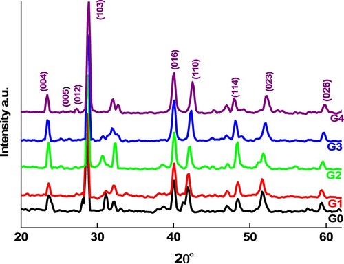
Through rising germanium accumulation, the large (103) peak represents a small red shift and decreases in intensity (except x = 5), demonstrating that crystallization is suppressed and particle size reduces. Average crystallite size (Cs) shown in Table has been estimated using Sherrer’s formula [Citation32] after making correction for instrumental broadening. It has been discovered that as the concentration of germanium increases, the particle size decreases. Because of the stronger bonding of Ge–Se, Ge may enter into the lattice of Sb65Se35 and replace the location of Sb, further inhibiting grain growth. Decreasing the grain size properly not only maintains the high programming speed but also improves the memory cell’s reliability [Citation33]. It’s also worth noting that the dislocation density () grows as particle size decreases. When the dislocation density is considerably higher, it is claimed that the involvement of dislocations causes a rise in the semiconductor material’s band gap, given that the dislocations are isolated by a substantial degree than the interatomic distance [Citation34]. Obviously, Ge molar variation had an important impact on these two crystallographic parameters (Cs and δ), however the dislocation density varied inversely with crystallite size as shown in Table .
Table 1. EDS, XRD and optical band gap results of the synthesized alloys.
3.2. SEM and EDS analyses
FESEM and EDS analysis were used to analyze the morphological and compositional characterizations of the pristine and Ge-doped samples. Figure presents the morphologies of powders with varying levels of germanium. The present compounds have morphologies that are similar to well-defined particles with a thin and appreciably fine flake-like composition. Also, particles which are available in a variety of sizes, ranging from 144 to 120 nanometers could be visible for Ge-free and Ge-with samples as shown in Figure . This means that local Se sublattices in crystals are gradually replaced by Ge atoms with lower electronegativity than Se atoms, resulting in the formation of unique defect species. Furthermore, the average particle size appears to decrease as a result of germanium substitution, implying that increasing the ratio of doping is an efficient method for crystalline enhancement. These photos show agglomeration spherical aggregates of smaller individual nanoparticles of various sizes. These results are consistent with the XRD results. Due to the extreme fine particle sizes, there is number of grain boundaries, which could further play an important role in governing the electrical behaviour and optical scattering in a material [Citation35]. However, the size reduction may result in changes in material properties. The smallest particle size is, the best material’s hardness and yield strength, according to the Hall–Petch relation, additionally, the rise is inversely related to the square root of particle size [Citation36].
Figure 2. FE-SEM images of the samples were recorded with 20 K x magnification.
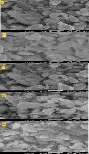
Figure 3. EDS spectra corresponding to the specimens.
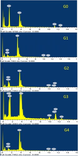
The compositions of the elements of Sb65Se35−xGex samples were investigated by using EDS as shown in Figure . Only Sb, Se, and Ge were detectable in the EDS spectra, suggesting that the synthesis was of high quality and the samples were pure. With an experimental error of 0.5%, the EDS data suggests that the real compositions of all samples are comparable to the nominal compositions (Table ).
3.3. Raman analysis
Raman spectroscopy is an effective and widely used characterization tool for determining atomic displacements and Raman essential vibrational modes, which can provide useful information about local disruptions and electrostatic distribution in the crystal structure of the probed material [Citation37–41]. Meanwhile, Raman spectra of Ge-doped Sb65Se35 samples offer a positive connection between structure evolution and ion replacement in Sb65Se35. Figure illustrates the compositional dependency of the room temperature Raman spectra of pure and Ge4+ substituted Sb65Se35 alloys, which are driven by several bands in the 80–200 cm−1 wave number range as previously reported [Citation27]. Nevertheless, the main bands in the Raman spectra of the examined specimens, which are located between 80–200 cm−1, could reflect inputs both from Sb–Se, Sb–Sb, and Ge–Se styles. This observation may show the existence of two fundamental crystal structures: SbSe3 pyramids and GeSe4 tetrahedrons. The qualitative compositional pattern of the peak integrals was monitored by comparing Raman data spectra with Lorentzian peaks. Table lists the characteristic parameters of each mode, including maximum point position (C), peak widening (W), relative area (A), and strength (I). These parameters were discovered to be dependent on the amount of Ge4+. The Raman shift and peak widening are influenced by crystallite size variation [Citation18]. Structure disorder can be linked to changes in these parameters [Citation42]. This could have an impact on the number of charge defect centres and, as a result, on electrical conductivity. Furthermore, the shifting in Raman modes is due to the lattice disorder caused by non-stoichiometry and the presence of internal stress in the material. It is possible that due to the high concentration of intrinsic structural defects caused by local inhomogeneities, there exists a high degree of disorder in the cation sublattice, resulting in the change of the space symmetry. Furthermore, non-stoichiometry and the existence of internal stress in the material generate lattice distortion, which causes Raman modes to shift. It’s probable that a large degree of disorder exists in the matrix as a result of the high concentration of intrinsic structural defects created by local inhomogeneities [Citation43].
Figure 4. Raman spectra of Ge-incorporated Sb65Se35 (0 ≤ x ≤ 20) samples.
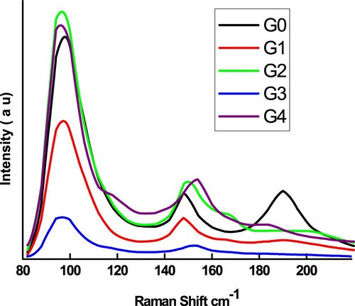
Table 2. The characteristic parameters of each mode, including relative area (A), maximum point position (C), peak widening (W), and relative intensity (I/Io) of Raman peaks of compositions.
3.4. Optical properties
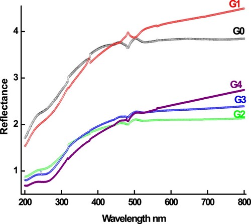
For practical application in the field of data storage, one of the most important optical characteristics of the material is optical band gap (Eopt) which is essential for the design and optimization of optical devices. Using diffuse reflectance (DR) spectra obtained from weakly absorbing samples, Kubelka and Munk (KM) proposed a model to evaluate the Eopt from fundamental edge. Despite, the reality that the DR technique is not as sensitive to tiny variations in optical properties of materials as the UV-Vis absorption technique, it can precisely extract the band gap values of powdered, crystalline, and nanostructure materials. At any wavelength, the KM equation is expressed as follows [Citation44]: , where R denotes reflectivity. The UV-Vis reflectance of all samples is plotted against wavelength in Figure . The diffused reflectance of undoped and doped samples clearly increased as the wavelengths were increased. Furthermore, the introduction of Ge dopant into the host Sb65Se35 causes a reduction in diffused reflectance. The absorption edges of pure, 5, 10, 15, and 20 Ge-doped Sb65Se35 are observed to initiate at 394, 404, 413, 380, and 369 nm, respectively. In other words, all curves contain similar shapes and absorption edges, and the wide absorption band is located in the region of 360–420 nm, where visible light absorption indicates to be heavy both for pure and doped Sb65Se35 alloys. As the concentration of Ge in the Sb65Se35 varies, so should the absorption edge of different samples.
Figure 5. Wavelength dependence of the reflectance for all compositions.
The absorption coefficient (α) and optical band gap (Eopt) [Citation45] in an indirect transition semiconductor are related as follows: , where hν is photon energy and B is a proportionality constant. The expression [Citation46]:
is obtained by evaluating the optical absorption coefficient (α = F(R)) from (KM). The values of the indirect band gap (Eopt) can be established by plotting [F(R)hν]0.5 against hν, and the intercept on the energy axis with zero absorbance, as shown in Figure . With increasing Ge doping, the Eopt raises from 0.48 to 1.48 eV depending on the geranium ratio as listed in Table . The increasing trend in Eopt would lead to a decrease in carriers and a reduction in carrier density, exposing an increment in the materials’ resistance. As a result of this observation and hypothesis, Ge dopant will alter Eopt and thus develop resistance [Citation22]. In general, carrier mobility is influenced by a variety of factors, but scattering at grain interfaces is likely to play the most essential role in the present case.
Figure 6. The relationship between the absorption coefficient and energy for various alloys.
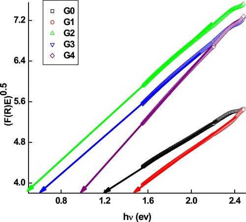
Because Ge ions are incorporated into the Sb65Se35 lattice, the band structure changes, causing modifications in the absorption peak position. It should also be mentioned that when the concentration of dopant increases, the grain size reduces, which could be another reason for the increased band gap. Previous research [Citation47] has found that the quantum confinement causes a shift in band gap in semiconductor nanoparticles below 10 nm. The particle sizes in this case are substantially larger and do not fall into the quantum confinement regime. As a result, the considerable blue-shift is produced by a change in band structure caused by the insertion of Ge4+ ions into the lattice.
3.5. Electrical properties
To further investigate the usefulness of Sb65Se35−xGex alloys for phase change memory applications, the electrical conductivity (σ) is based on the measurement of temperatures ranging from 100 to 400 K. Figure shows the variance of the σ − T curves for the investigated compounds. The electrical conductivity seems to be primarily affected by the nominal composition, as according to these curves. However, as the temperature rises, decreases monotonically, trying to suggest a degenerate semiconductor characteristic. The same kind of semiconductor behaviour has been reported in other works [Citation48–50], which may be due to the varying Fermi surfaces of the paramagnetic and ferromagnetic types. The wave vector transferred in a scattering process through the Fermi level in the ferromagnetic phase is greater than in the paramagnetic phase, and hence the conductivity in the paramagnetic phase is weaker than it does in the ferromagnetic phase. The electrical conductivity of pristine sample is the smallest. With increasing germanium content, the electrical conductivity shows a non-monotonic increase. Moreover, the σ of doped samples is higher than the undoped one. The electrical conductivity is given by , where n, e and μ are the carrier concentration, the electron charge and the carrier mobility, respectively [Citation51]. It means that σ should be affected by the simultaneous variation of n and μ. A higher carrier mobility will result in a large electrical conductivity. Moreover, the increase in electrical parameter when Ge concentration in Sb65Se35 samples grows could be due to two factors. To begin with, when the concentration of Ge ions in the Sb65Se35 lattice increases, the Ge ions offer an excess of free electrons in the lattice, which increases electrical conductivity. The Ge ions in the Sb65Se35 lattice are thought to act as charge carriers and acceptor impurities. Second, when the concentration of Ge increases, the Ge atoms make more neck contact with Se sites, speeding charge carrier movement and thereby boosting conductivity. This behaviour is explained by the crystal lattice defect model, which assumes that Ge atoms interact with native defects in the crystal lattice of undoped Sb2Se, specifically antisite defects Sb′Se and V′Se. The chance of new anti-site defects occurring and the concentration of free electrons growing as a result of the increasing germanium content [Citation52,Citation53]. Nevertheless, raising Ge content causes impurity levels to expand due to the narrow band-gap of pure Sb2Se, where donor and acceptor levels are extraordinarily close to the conduction and valence band edges [Citation54,Citation55].
Figure 7. Electrical conductivity (σ) as a function of temperature for various compounds.
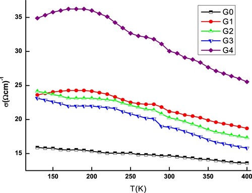
The bond polarity contributes to the formation of antisite defects in Sb65Se35-based crystals. The lower the polarity of the bond between positive and negative charged atoms, the more likely an antisite defect will form. Despite the fact that antisite defects have holes and can counteract electrons, the interaction of vacancies and antisite defects becomes the major player, resulting in further electrons [Citation56]. As a consequence, the carrier concentration rises as the particle size decreases. Furthermore, as particle size decreases, grain boundary, antisite defect, vacancy, and interface defects increase, resulting in greater carrier scattering. As a result, carrier mobility is restricted [Citation57,Citation58]. Overall, our findings show that the doping of Ge in Sb65Se35 is suitable method for achieving the potential of Sb65Se35-based materials in optoelectronic devices in the future.
4. Conclusion
Sb65Se35−xGex (x = 0–20) polycrystalline materials are produced. Ge content affects the morphology and crystallite size of the specimens. Raman spectroscopy investigations were performed out to see how compositional contributions made by Ge doping affect the lattice fluctuations and electron phonon associations in the system under examination. The introduction of Ge dopant into the host Sb65Se35 causes a reduction in diffused reflectance. With increasing Ge doping, the Eopt rises from 0.41 to 1.68 eV. The σ of all samples decreases monotonically as the temperature goes up, revealing a degenerate semiconductor characteristic. As a result of the Ge doping in Sb65Se35, fascinating optical properties in the visible region as well as enhanced electrical properties have been discovered. Because of its improved optical and electrical properties, Ge doping in Sb65Se35 system would be a suitable choice for electronic data storage in the future.
Disclosure statement
No potential conflict of interest was reported by the author(s).
Additional information
Funding
References
- Gao S, Hu Y, Wang L, et al. Simultaneously good thermal stability and low power consumption for Sb/In48.9Sb15.5Te35.6 multilayer composite film. J Non-Cryst Solids. 2021;567:120928.
- Xu M, Lu Y, Li Z, et al. Compositional optimization of binary selenium-antimony films for low-power electrical and optical storage. J Alloys Compd. 2018;740:477–484.
- Zou H, Zhu X, Hu Y, et al. Improving the thermal stability and phase change speed in Sb70Se30 films through Er doping. J Mater Sci Mater Electron. 2017;28:17719–17725.
- Sun Z, Zhou J, Shin H-J, et al. Stable nitride complex and molecular nitrogen in N doped amorphous Ge2Sb2Te5. Appl Phys Lett. 2008;93:241908.
- Chen L, Song S, Song Z, et al. Sb52Se36Te12 material with high-temperature data retention coupled with rapid crystallization speed for phase change application. Appl Surf Sci. 2015;357:603–607.
- Rao F, Song Z, Ren K, et al. Sn12Sb88 material for phase change memory. Appl Phys Lett. 2009;95:032105.
- Hu Y, Li S, Lai T, et al. Al19Sb54Se27 material for high stability and high-speed phase-change memory applications. Scr Mater. 2013;69:61–64.
- Eising G, Van Damme T, Kooi BJ. Unraveling crystal growth in GeSb phase-change films in between the glass-transition and melting temperatures. Cryst Growth Des. 2014;14:3392–3397.
- Putero M, Coulet M-V, Muller C, et al. Ge-doped GaSb thin films with zero mass density change upon crystallization for applications in phase change memories. Appl Phys Lett. 2016;108:101909.
- Zhang Z, Gu Y, Song S, et al. Investigation of Al-Sb-Se alloy for long data retention and low power consumption phase change memory application. J Appl Phys. 2014;116:074304.
- Yoon S-M, Lee N-Y, Ryu S-O, et al. Sb-Se-based phase-change memory device with lower power and higher speed operations. IEEE Electron Device Lett. 2006;27:445–447.
- Ji XL, Wu L, Zhou W, et al. High thermal stability Sb3Te-TiN2 material for phase change memory application. Appl Phys Lett. 2015;106:023118.
- Shen X, Wang G, Wang RP, et al. Enhanced thermal stability and electrical behavior of Zn-doped Sb2Te films for phase change memory application. Appl Phys Lett. 2013;102:131902.
- Matsunaga T, Yamada N. Structural investigation of GeSb2Te4: a high-speed phase-change material. Phys Rev B. 2004;69:104111.
- Yousaf SA, Ikram M, Ali S. Compositional engineering of acceptors for highly efficient bulk heterojunction hybrid organic solar cells. J Colloid Interface Sci. 2018;527:172–179.
- Ahmad SOA, Ashfaq A, Akbar MU, et al. Application of two-dimensional materials in perovskite solar cells: recent progress, challenges, and prospective solutions. J Mater Chem C. 2021;9:14065–14092.
- Salam W, Ikram M, Shahzadi I, et al. Doping dependent structural, optical, thermal and catalysis properties of synthesized cadmium sulfide nanoparticles. Nanosci Nanotechn Lett. 2018;10:1662–1670.
- Zaidi AA, Rafique MS, Aslam S, et al. Effects of solvents on structural, optical and photovoltaic properties of photo anodes for dye-sensitized solar cells. Optik (Stuttg). 2020;200:163444.
- Yousaf SA, Imran M, Ikram M, et al. The critical role of metal oxide electron transport layer for perovskite solar cell. Appl Nanosci. 2018;8:1515–1522.
- Imran M, Ikram M, Anjum S, et al. Highly efficient hybrid bulk heterojunction organic solar cells integrating PbS nanoparticles. Nanosci Nanotechn Lett. 2018;10:1644–1650.
- Chen Y, Wang G, Tian M, et al. Fast reversible laser-induced crystallization of Sb-rich Zn-Sb-Se phase change material with excellent stability. AIP Adv. 2015;5:077174.
- Zou H, Zhu X, Hu Y, et al. Improving the thermal stability and phase change speed in Sb70Se30 films through Er doping. J Mater Sci Mater Electron. 2017;28:17719–17725.
- Lu Y, Song S, Song Z, et al. Ga14Sb86 film for ultralong data retention phase-change memory. J Appl Phys. 2011;109:064503.
- Lu Y, Song S, Shen X, et al. Phase change characteristics of Sb-rich Ga–Sb–Se materials. J Alloys Compd. 2014;586:669–673.
- Liu R, Hu A, Zhao Z, et al. Zn-doped Sb70Se30 thin films with multiple phase transition for high storage density and low power consumption phase change memory applications. Scr Mater. 2020;178:324–328.
- Liu G, Wu L, Zhu M, et al. The investigations of characteristics of Sb2Te as a base phase-change material. Solid-State Electron. 2017;135:31–36.
- Saleh SA. Synthesis and characterization of Sb65Se35-xGex alloys. Mater Sci Appl. 2011;2:950–956.
- Kang TD, Sirenko A, Park J-W, et al. Investigation of the structural and optical properties of Ge-doped SbTe films with various Sb:Te ratios. J Electrochem Soc. 2011;158:H249.
- Prokhorov E, Mendoza-Galván A, González-Hernández J, et al. Effects of Ge addition on the optical and electrical properties of eutectic Sb70Te30 films. J Non-Cryst Solids. 2007;353:2125.
- Denton AR, Ashcroft NW. Vegard’s law. Phys Rev A At Mol Opt Phys. 1991;43:3161–3164.
- González-Hernández J, Chao BS, Strand D, et al. Crystallization studies of Ge: Sb: Te optical memory materials. Appl Phys Comm. 1992;11:557–581.
- Cao Y, Zhu P, Shi W, et al. Correlation between X-ray diffraction pattern and microstructure of surface of E690 high-strength steel induced by laser-shock processing. Vacuum. 2022;195:110595.
- Gu Y, Song S, Song Z, et al. Phase-change material Ge0.61Sb2Te for application in high-speed phase change random access memory. Appl Phys Lett. 2013;102:103110.
- Saleh SA. Preparation of degenerate n-type Sb65GexSe35-x alloys with a small grain size and their thermoelectric properties. J Phys. 2013;2:4–11.
- Ameer S, Jindal K, Sharma S, et al. Structural, morphological and optical properties of BiFe0.99Cr0.01O3 thin films. Vacuum. 2018;158:166–171.
- Shi X, Feng X, Teng J, et al. Effect of laser shock peening on microstructure and fatigue properties of thin-wall welded Ti-6A1-4V alloy. Vacuum. 2021;184:109986.
- Saleh SA. Study of microstructural, electrical and dielectric properties of La0.9Pb0.1MnO3 and La0.8Y0.1Pb0.1MnO3 ceramics. Guigoz Sci Rev. 2019;5:33–44.
- Muneeswaran M, Lee SH, Kim DH, et al. Structural, vibrational, and enhanced magneto-electric coupling in Ho-substituted BiFeO3. J Alloys Compd 2018;750:276–285.
- Guo S, Huang T, Xu LP, et al. Observation of an intermediate phase in tungsten doped Sb2Te phase change thin films by temperature dependent measurements of structural, optical, and electronic properties. J Phys D: Appl Phys. 2016;49:265105.
- Beekman C, Reijnders AA, Oh YS, et al. Raman study of the phonon symmetries in BiFeO3 single crystals. Phys Rev B. 2012;86:020403(R).
- M.N. Iliev, Abrashev M. V., Mazumdar D., Shelke V., Gupta A., Polarized Raman spectroscopy of nearly tetragonal BiFeO3 thin films Phys Rev B 82 (2010) 014107.
- Saleh SA, Al-Hajry A, Ali HM. Structural and optical properties of Sb65Se35−xGex thin films. Phys Scr. 2011;84:015604.
- Chandel T, Zaman MB, Dwivedi SK, et al. Structural, morphological and optical properties of sprayed Cu2ZnSnS4 thin films by varying the molar concentration of Zn & Sn. Vacuum. 2019;159:341–445.
- Saleh SA, Ibrahim AA, Mohamed SH. Structural and optical properties of nanostructured Fe-doped SnO2. Acta Phys Polinica A. 2016;126:1220–1225.
- Imran MMA, Lafi OA, Abu-Samak M. Effect of thermal annealing on some electrical properties and optical band gap of vacuum evaporated Se65Ga30In5 thin films. Vacuum. 2012;86:1589–1594.
- Ali HM, Saleh SA. Growth and opto-electro-structural properties of nanocrystalline PbSe thin films. Thin Solid Films. 2014;556:552–559.
- Sinha AK. Band gap energy calculation of cobalt doped bismuth ferrite nanoparticles. Mater Today Proc. 2021;42:1519–1521.
- Hsu KF, Loo S, Guo F, et al. Cubic AgPbmSbTe2+m: bulk thermoelectric materials with high figure of merit. Science. 2004;303:818–821.
- Ibrahim MM, Ibrahim EMM, Saleh SA, et al. Synthesis and characterization of semimagnetic semiconductor Pb1−xSmxSe. J Alloys Compd. 2007;429:19.
- Figiel H, Budziak A, Żukrowski J, et al. Neutron diffraction studies of TbMn2Dx and ErMn2D2. J Mag Mag Mater. 2004;272–276:585–586.
- Lv T, Li Z, Liu Y, et al. Improving thermoelectric performance of (Bi0.2Sb0.8)2(Te0.97Se0.03)3 via Sm-doping. J Alloys Compd. 2019;787:909–917.
- LoŠŤák P, Horák J, Navrátil J, et al. Properties of Bi2Se3 single crystals doped with Pb atoms. Phys Stat Sol A. 1993;136:K121–K125.
- Plecháček T, Navrátil J, Horák J, et al. Defect structure of Pb-doped Bi2Te3 single crystals. Phil Mag. 2004;84:2217–2228.
- Soni A, Yanyuan Z, Ligen Y, et al. Enhanced thermoelectric properties of solution grown Bi2Te3–xSex nanoplatelet composites. Nano Lett. 2012;12:1203–1209.
- Ivanovaa LD, Petrova LI, Granatkina YV, et al. Extruded thermoelectric materials based on Bi2Te3-Bi2Se3 solid solutions. Inorg Mater. 2009;45:123–128.
- Son JH, Oh MW, Kim BS, et al. Effect of ball milling time on the thermoelectric properties of p-type (Bi,Sb)2Te3. J Alloy Compd. 2013;566:168–174.
- Zhang C, Fan XA, Hu J, et al. Changing the band gaps by controlling the distribution of initial particle size to improve the power factor of N-type Bi2Te3 based polycrystalline bulks. Adv Eng Mater. 2017;19:1600696.
- Bruncko J, Šutta P, Netrvalová M, et al. Pulsed laser deposition of Ga doped ZnO films – influence of deposition temperature and laser pulse frequency on structural, optical and electrical properties. Vacuum. 2019;159:134–140.