
 ?Mathematical formulae have been encoded as MathML and are displayed in this HTML version using MathJax in order to improve their display. Uncheck the box to turn MathJax off. This feature requires Javascript. Click on a formula to zoom.
Abstract
The inverse problem of optical coatings control during their deposition is an important practical and industrial problem. The paper presents the mathematical investigation of the layer thickness errors self-compensation effect that is quite important for the quality production of modern types of thin film optical coatings. It studies the mechanism of thickness errors correlation in the case of direct monitoring of optical coating production by broadband online spectral photometric devices. The mathematical description of this mechanism is provided. The obtained results make it possible to predict the existence of a strong error self-compensation effect when theoretical optical coating design and parameters of the monitoring procedure are known. Mathematical results of the conducted research are confirmed by computational experiments with the data obtained for the optical coating design problem where a very strong error self-compensation effect has been practically observed.
1. Introduction
Optical coating technology is one of the key modern technologies with products turnover counted in billions of dollars. Thin film optical coatings surround us in our everyday life as elements of ophthalmology lenses, smartphones, photo cameras, various displays, protective structures of currency bills, etc. [Citation1,2]. They are used as essential elements of all lasers, medical instrumentation, various sensors, lenses for laser lithography, advanced optical and X-ray telescopes and so on. In recent years, tremendous progress has been achieved both in development of new deposition techniques used for the production of optical coatings [Citation2] and in development of mathematical methods used for solving inverse problems of designing optical coatings with required spectral properties [Citation3].
Mathematical methods for solving inverse problem of designing optical coatings are based on the optimization of a merit function that estimates proximity of spectral characteristic of a designed coating to the specified target spectral characteristic in a given spectral range [Citation4]. Optimization parameters, also called design parameters, are usually thicknesses of optical coating layers. Modern deposition techniques allow one to produce coatings with many dozens and even hundreds of layers. For example, coatings for the wavelength division-multiplexing (WDM) applications may have several hundreds of layers. Thus the numbers of optimization (design) parameters may be very high. The merit function is non-convex and for many years its optimization using various non-local optimization methods presented the main challenge in the development of new types of optical coatings. A breakthrough in the merit function optimization was achieved due to the invention of a special non-convex optimization technique called the needle optimization technique [Citation5]. Nowadays a set of general purpose optimization approaches based on this technique and a set of specialized design methods [Citation3,6,7] allow solving the problems of optical coating design even in the cases when many hundreds of optimization parameters are used. Now the key issue for further progress in optical coatings is bringing together outstanding capabilities of modern mathematical design methods and modern deposition techniques. In this respect the most important issue is an application of a proper monitoring technique that provides an accurate control of coating layer thicknesses during their deposition.
There is a great variety of monitoring techniques for optical coatings production, all of them having their pros et contras [Citation8]. At present the so-called direct optical monitoring techniques are considered as the most promising ones in the case of deposition of the most challenging optical coatings. For example, the production of filters for WDM applications is only possible with the direct monochromatic optical monitoring at the central wavelength of the filter pass band [Citation9]. It turns out that even atomic level errors in layer thicknesses of WDM filters entirely destroy spectral properties of such filters. Actual errors in deposited layer thicknesses are many times higher than the characteristic atomic dimensions of several tenths of a nanometer; nevertheless WDM filters are successfully produced when the mentioned monitoring technique is applied. The reason for this surprising fact is the so-called error self-compensation mechanism associated with the chosen type of monitoring technique that reveals itself when WDM filters and other types of narrow band pass filters are produced [Citation9]. Unfortunately in the case of monochromatic optical monitoring this effect is not observed for coatings of other types.
In recent years various broadband monitoring (BBM) techniques have gained essential attention [Citation8]. They are based on measuring transmittance or reflectance spectra of the deposited coating inside the production chamber at short time intervals in which only small fractions of coating layers are deposited. Measured spectra are used as input data for the inverse problem of determining thickness of the growing layer. Layer deposition is terminated when layer thickness reaches the required value corresponding to the layer thickness of a theoretical coating design. In the case of direct BBM all spectral measurements are performed only on one of the samples located inside the deposition chamber. The first system of this type was developed almost 40 years ago [Citation10–12], and even at that time the main pros et contras of direct BBM were outlined. It was noticed that this type of monitoring may give a rise to a cumulative effect of rapid growth of thickness errors with the growing number of deposited layers. On the other hand it was supposed that some kind of error self-compensation mechanism may be associated with direct BBM. An accurate mathematical investigation of these effects was performed many years later [Citation13,14] and it was confirmed that both effects really exist.
In the case of direct BBM the errors in previously deposited layers influence measured spectra of the layer that is currently deposited. These spectra are used for the online determination of the growing layer thickness and for the prediction of the deposition termination instant. As a result the error in the thickness of this new layer turns out to be correlated with the errors in all previously deposited layers. The correlation of thickness errors causes a negative effect of thickness errors accumulation [Citation13] but it may also cause a positive effect of error self-compensation [Citation14].
Tikhonravov et al. [Citation14] proposed the following approach to check the presence of the error self-compensation effect and to estimate its strength. A series of computational experiments simulating a real deposition process with direct BBM is performed [Citation15]. As a result several sets of correlated thickness errors are obtained and standard deviations of thickness errors for all coating layers are calculated. Then several sets of normally distributed uncorrelated thickness errors with the same standard deviations are generated. The influence of correlated and uncorrelated thickness errors on a coating spectral characteristic is estimated by the mean-square deviation of this characteristic from the spectral characteristic of theoretical coating design without thickness errors. Such mean-square deviations are calculated for all sets of correlated thickness errors and their mean value Mcorr is found. Then the same values are calculated for all sets of uncorrelated thickness errors and again respective mean value Mnon-corr is found. The ratio S = Mnon-corr/Mcorr is the criterion for the presence of the error self-compensation effect; the effect is present if S > 1. Obviously, the error self-compensation effect is stronger when S value is high. In the paper [Citation14] various types of optical coatings were investigated and it was found that S values exceeded 1 in all situations, i.e. some error self-compensation effect was always present. However the strength of this effect was quite different for different types of optical coatings. In the mentioned experiments S values varied in the range from 1.6 to 15.9.
Recently the presence of a very strong error self-compensation effect in the case of coating deposition with direct BBM was practically demonstrated by the production of Brewster-angle polarizers for high energy laser optics [Citation16]. The polarizers described in this paper are key thin film elements for laser fusion optics [Citation17] and the application of direct BBM for the control of their deposition opens new horizons in manufacturing these quite expensive products. The results reported in [Citation16] give a new stimulus for mathematical investigation of the error self-compensation mechanism associated with direct BBM of optical coating production. The main goal of the present work is to reveal the origin of this effect and to provide the mathematical algorithm that would allow one to predict its presence when coating structure and specific parameters of direct BBM procedure are known. In Section 2 formulations of the inverse problem of optical coating designing and of the inverse problem of layer thickness control with direct BBM are presented. Section 3 is devoted to mathematical investigation of the origin of the error self-compensation mechanism. In Section 4 the main results of the previous section are illustrated and supported by the computational experiments with the polarizer design from [Citation16]. Final conclusions are presented in Section 5.
2. Formulation of the inverse problem of optical coating designing and of the inverse problem of thickness monitoring
We start this section with the formulation of the direct problem in thin film optics. The direct problem is formulated for the simplest case of normal light incidence and considering only one optical coating spectral characteristic, namely its spectral transmittance. Formulations of the direct problem in more general cases can be found in the book [Citation4]. The necessary pages of this book are also available at www.optilayer.com [Citation18]
Let d1, …, dm be physical thicknesses of coating layers and n1, …, nm be refractive indices of these layers. Intensity transmission coefficient or transmittance of an optical coating is calculated using the following formulas.
First the so-called characteristics matrices of coating layers are formed. These are 2 by 2 matrices:(1)
(1)
Here j is the number of the coating layer counting from the substrate on which the coating is deposited, λ is the wavelength of the incident light, and i is the imaginary unit.
The product of layer characteristic matrices is called the characteristic matrix of optical coating:(2)
(2)
In Equation (2) m is the total number of deposited layers. The elements of this 2 by 2 complex matrix mkl are used to calculate the transmittance of optical coating:(3)
(3)
In this equation na is the refractive index of the incident medium where the incident wave comes from, and ns is the refractive index of the substrate. The transmittance depends on the wavelength of the incident wave which enters Equation (1) as a parameter.
Analogous recurrent formulas are used to calculate all other spectral characteristics. In the case of oblique light incidence, pairs of spectral characteristics for s- and p-polarized light are considered (s- and p-polarization cases differ in the orientations of electric vectors of the incident electromagnetic wave with respect to the plane of incidence [Citation4]).
The inverse problem of optical coating designing is formulated based on specified target spectral characteristics of the optical coating. As an example, we consider the inverse problem of designing a polarizer that is used in Section 4 to illustrate mathematical results of Section 3. The target spectral characteristics for the polarizer are specified for a given incidence angle in the spectral range around the laser wavelength where polarization effect must be provided. In the paper [Citation16] the polarizer for the incidence angle of 55.6° and laser wavelength of 1064 nm is considered; polarizer spectral range is 30 nm around the laser wavelength. In this spectral range the target transmittance for the p-polarized light Tp is 1 and the target transmittance for the s-polarized light Ts is 0. The inverse design problem is formulated as a problem of optimizing the functional(4)
(4)
In Equation (4) the summation is made over the wavelength grid with 1 nm step in the polarizer spectral range.
In thin film optics the functional given by Equation (4) is called merit function and we will further use this term to distinguish it from the functionals that will be introduced later in connection with thickness monitoring. Optimization parameters for the merit function are thicknesses of coating layers. Refractive indices of these layers are predefined because polarizer consists of the layers with two alternating refractive indices formed by successive deposition of two thin film materials [Citation16].
The discussion of modern optimization methods used in thin film optics is beyond the scope of this paper. We only mention that methods based on the needle optimization technique [Citation3,5–7] do not limit the dimension of the space of optimised parameters. This approach entirely corresponds to the modern paradigm of optical coating designing that requires taking into consideration a number of poorly formulated practical demands. Anyway, all methods based on the needle optimization technique construct optical coating designs with parameters providing a minimum of the optimized merit function. Thus in all cases merit function gradients are equal to zero. This is an important note for the considerations of Section 3.
Let us turn our attention to the inverse problem of thickness monitoring. In the case of direct BBM the following functional is used to control the thickness of the deposited layer:(5)
(5)
Here j is the number of the layer being deposited, is the measured transmittance spectrum acquired by optical monitoring device at a certain measurement instant,
is the theoretical transmittance spectrum expected at the end of the j-th layer deposition. It is typical that in the case of direct BBM normal incidence transmittance spectra are used to control the coating deposition. Summation in Equation (5) is performed over the wavelength grid where an optical monitoring sensor records online monitoring spectra. Usually this grid covers a fairly broad spectral range and has many hundreds or even thousands of wavelength points. For example, in the study [Citation16] online normal incidence transmittance spectra were collected at 2036 wavelength points in the spectral range from 658 to 1172 nm. It is worth noting that spectral grids in Equations (4) and (5) may be absolutely different and incidence angles of spectral characteristics in these equations may also be different.
Let us denote layer thicknesses of the theoretical coating design provided by the merit function optimization. In Equation (5) all theoretical transmittance spectra
are entirely specified by the
values. When the j-th layer is deposited the measured transmittance spectrum
in Equation (5) varies with the growth of the thickness of this layer dj. Further in the text we indicate dependence of transmittance spectra on this parameter and omit indicating an obvious dependence of transmittance data on the wavelength. The measured transmittance spectrum can be represented in the form
(6)
(6)
where are actual thicknesses of the previously deposited layers with the numbers from 1 to j-1 and
are errors in measured transmittance data.
Measured transmittance spectra are acquired online at short time intervals of one to several seconds in which only a small fraction of the growing layer is deposited. The deposition of the j-th layer is terminated at an instant when the functional (5) reaches a minimum. Technical details of algorithms used for determining termination instants are not important for our considerations and for this reason are not discussed here. For the following considerations the most important fact associated with solving the inverse problem of thickness monitoring is that the thickness of the j-th layer dj corresponds to the minimum of the functional (5):(7)
(7)
3. Mathematical investigation of the origin of error self-compensation mechanism
Errors in the deposited layer thicknesses cause variations of the merit function F used for solving the inverse problem of optical coating designing. Denote δd1, …, δdm deviations of actual layer thicknesses from the layer thicknesses of theoretical design
. For the theoretical design the merit function gradient is equal to zero and the merit function variation caused by the errors δdj is equal to
(8)
(8)
Let us introduce the matrix(9)
(9)
and the column vector Δ whose elements are thickness errors δdj. We can rewrite Equation (8) as(10)
(10)
Let Λ be the diagonal matrix composed of the matrix A eigenvalues in descending order. Introducing matrix Q whose columns are matrix A eigenvectors we can write down the eigen decomposition of matrix A:(11)
(11)
We can rewrite Equation (10) in the form(12)
(12)
where the column vector H is(13)
(13)
The elements hi of the vector H are linear combinations of the thickness errors δdj. Suppose that only a few matrix A eigenvalues λi noticeably differ from zero. Let the number of these eigenvalues be I. We can write down the following approximate equation(14)
(14)
Suppose now that layer thickness errors are correlated by the monitoring procedure so that all linear combinations hi in Equation (14) are zero or close to zero. In this case the merit function variation is also close to zero and thus the error self-compensation effect is observed. Our next goal is to understand when the direct BBM procedure correlates thickness errors in such a way.
Consider the functional Фj(d) in the right hand part of Equation (7). Recall that the deposition of the layer number j is terminated when the minimum of this functional with respect to the thickness of the j-th layer dj is achieved. Assuming that all variations of layer thicknesses from the theoretical layer thicknesses are small, we can write in the first approximation(15)
(15)
Here, δd1, …, δdj-1 are thickness errors that have been already made during the depositions of previous layers and (16)
(16)
is the deviation of the j-th layer thickness from the planned theoretical value.
The functional Фj(d) is quadratic with respect to the thickness errors and we can rewrite it in the form(17)
(17)
It has been already mentioned that BBM spectra are acquired on large spectral grids with many hundreds or even thousands of spectral points. The derivatives of the transmittance coefficients are smooth functions of the wavelength. In many situations measurement errors δTmeas can be considered as normally distributed random errors and summation of the terms
over the wavelength grid give values that are close to zero. This means that in the following considerations we can neglect the second term in the right-hand part of Equation (17) and assume that the minimum of Фj(d) is achieved when the first term in the right-hand part of this equation acquires its minimum value.
Let us introduce the matrix(18)
(18)
and the column vector(19)
(19)
According to the above considerations the deposition of the j-th layer is terminated when the minimum value of the quadratic form(20)
(20)
is achieved.
We can consider Equation (20) as the equation describing the mechanism of correlating the j-th layer thickness error δdj with the thickness errors that have been already made during the depositions of previous layers.
Let Vj be the diagonal matrix whose elements are the eigenvalues of matrix Cj in descending order. Introducing the matrix Pj whose columns are matrix Cj eigenvectors we can write down Equation (20) in the form:(21)
(21)
To make the main idea of our considerations more distinct let us assume that only a few eigenvalues of the matrix Cj noticeably differ from zero and that we can replace all small eigenvalues in Equation (21) by zeros. In fact this assumption proves to be fair in the situation when a strong error-self compensation effect is observed in practice (see Section 4).
Let be the non-zero eigenvalues in Equation (21) and
be the respective eigenvectors of this matrix. We can rewrite Equation (21) as
(22)
(22)
Let be elements of one of the eigenvectors
. Consider the m-coordinate row vector Wij with the coordinates
(23)
(23)
Obviously the scalar product in the square brackets of Equation (22) can be written down as(24)
(24)
and Equation (23) can be represented as(25)
(25)
Recall that this equation is obtained from Equation (20) describing the mechanism of thickness errors correlation.
Consider now all row vectors Wij obtained in the way described above. These vectors are formed for the numbers j starting from j = 2 because the correlation of thickness errors starts with the deposition of layer number 2. For each j > 2 there may be several vectors Wij with the numbers i from 1 to kj (see above). In general, one should expect that the total number of row vectors Wij significantly exceeds the total number of layers m. Nevertheless, to highlight the main idea of the following considerations, let us assume for a moment that all row vectors Wij belong to the subspace of Rm with the dimension smaller than m. Denote this subspace as P and its orthogonal complement as P⊥.
Errors in the deposited layer thicknesses are caused by multiple factors [Citation15] and always contain random components. For this reason the error vector Δ whose components are correlated by direct BBM also have a random nature and may significantly vary from one deposition run to another. According to Equation (25) direct BBM correlates thickness errors in such a way that the error vector tends to be orthogonal to the subspace P and hence Δ is expected to belong to its orthogonal complement P⊥.
Recall now the main conclusion based on Equation (14). It was indicated that the error self-compensation effect is observed if all linear combinations hi in Equation (14) are zero or close to zero. These linear combinations are scalar products(26)
(26)
where Qi are eigenvectors of the matrix A.
The linear combinations hi in Equation (14) correspond to the main I eigenvalues of the matrix A that have non-negligible values. Suppose that all eigenvectors Qi for i from 1 to I belong to the subspace P. Then all hi in Equation (26) are equal to zero which means that the merit function is not influenced by the thickness errors, i.e. that the error self-compensation effect is present.
The above simplified consideration indicates the way to investigating the presence of the error self-compensation effect in general case when the linear span of vectors Wij coincides with the whole space Rm. Let us compose the matrix W whose rows are row vectors Wij. This is the matrix of the dimension k × m where k is the total number of all row vectors Wij. According to the above considerations one should expect that k exceeds m noticeably. Let us also compose the matrix by adding I row vectors
to the matrix W. This is (k + I) by m matrix.
Consider the singular value decomposition (SVD) of the matrix W:(27)
(27)
Here U is a k × k unitary matrix, V is an m × m unitary matrix, and Σ is a k × m rectangular diagonal matrix with non-negative real numbers on its diagonal (singular values of the matrix W).
Consider also the SVD of the matrix :
(28)
(28)
Singular values of the matrices W and are arranged in descending order. Suppose that only s < m first singular values are noticeably different from zero. In this case one should expect that thickness errors correlated by the monitoring procedure form the vector Δ that is ‘nearly orthogonal’ to the s-dimensional span of the matrix V columns corresponding to the main s non-negligible singular values. Suppose then that the matrix
has the same number s of non-negligible singular values and these values are nearly the same as the first s singular values of the matrix W. This means that all vectors Qi for i from 1 to I are close to their projections on the subspace formed by the matrix V columns corresponding to the main s singular values. As a sequence scalar products
are close to zero and the error self-compensation effect is present. The next section presents results of computational experiments that completely support the conclusions made in this section.
4. Computational experiments with polarizer design
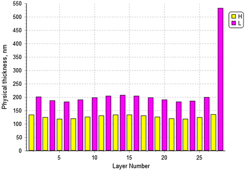
Computational experiments of this section are performed for the polarizer design that practically demonstrated the presence of a very strong error self-compensation effect [Citation16]. This polarizer has 28 layers formed by ZrO2 and SiO2 thin film materials. Refractive indices of these materials in the polarizer working spectral zone around 1064 nm are about 2.02 and 1.45, respectively. Polarizer is deposited on the glass substrate and its first layer from the substrate is the high index ZrO2 layer. Layer physical thicknesses of the discussed polarizer are presented in Figure .
Figure 1. Layer physical thicknesses of the 28-layer polarizer.
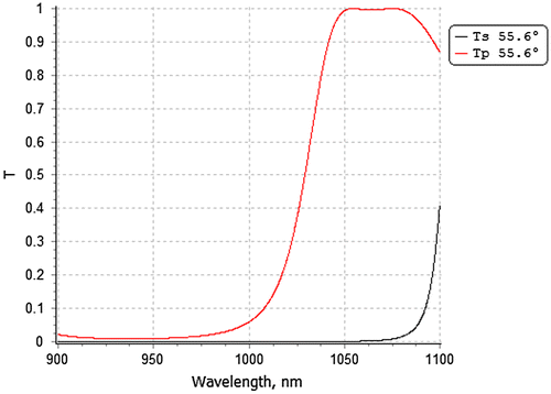
The polarizer target spectral characteristics Tp = 1 and Ts = 0 are specified for the 55.6° angle of light incidence at 31 wavelength points with 1 nm step in the spectral range around the 1064 nm laser wavelength. Theoretical spectral characteristics of the polarizer design without thickness errors are shown in Figure .
Figure 2. Ts and Tp transmittances of the theoretical polarizer design.
In the paper [Citation16] direct BBM of polarizer layer thicknesses was performed by measuring normal incidence transmittance data at 2036 spectral points in the wavelength region from 658 to 1172 nm. Transmittance spectra acquired at the end of each layer deposition are stored and used later for solving the inverse problem of post-production characterization [Citation19]. This problem is formulated as the determination of actual layer thicknesses of the deposited coating using online spectra recorded at the end of each coating layer deposition. In our case there are 28 unknown parameters and input data is represented by 28 transmittance spectra each having 2036 data points. For solving this inverse problem the so-called triangular algorithm is applied [Citation20]. This algorithm has proved to be fairly reliable for solving inverse problems of layer thicknesses determination. Figure presents thickness errors calculated for one of the deposited polarizers [Citation16].
Figure 3. Errors in the thicknesses of produced polarizer.
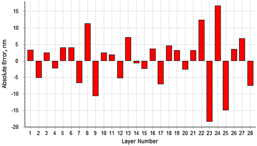
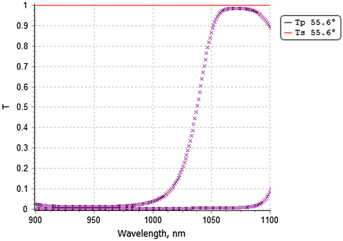
The thickness errors presented in Figure are quite high. This was demonstrated by the series of 1000 computational experiments with uncorrelated thickness errors performed in [Citation16]. Errors in layer thicknesses were simulated using normal distribution of thickness errors with zero mathematical expectations and standard deviations equal to modules of thickness errors shown in Figure . Figure presents mathematical expectation and the standard deviation corridor for the Tp transmittances calculated in these experiments. It can be seen that in the case of uncorrelated thickness errors spectral properties of the Tp transmittance are entirely destroyed. It is therefore amazing that correlated thickness errors shown in Figure do not destroy polarizer spectral properties. The measured spectral characteristics of the produced polarizer are shown in Figure .
Figure 4. Mathematical expectation and corridor of deviations for the Tp transmittance calculated based on the experiments with non-correlated thickness errors [Citation16].
![Figure 4. Mathematical expectation and corridor of deviations for the Tp transmittance calculated based on the experiments with non-correlated thickness errors [Citation16].](/cms/asset/9cc204cb-dd65-4aa4-8ac1-b35af2585a28/gipe_a_1395424_f0004_oc.gif)
Figure 5. Measured s- and p-transmittances of the produced polarizer.
Results presented in Figure vividly demonstrate the practical importance of the error self-compensation effect. This effect is very strong in the case of polarizer design and monitoring procedure considered in [Citation16]. The following discussion shows that this fact fully complies with the mathematical results of the previous section.
Let’s start with the matrix A of the polarizer merit function given by Equation (4). Indeed, only a small number of its eigenvalues is needed to write the approximate Equation (14). The three largest eigenvalues of this matrix are 9.33 × 10⁻⁴, 5.83 × 10⁻⁴ and 3.95 × 10⁻⁴. All other eigenvalues are smaller than one hundredth of the first one. For this reason only three first matrix A eigenvectors will be used later to form the matrix .
It is worth mentioning now that – in accordance with the prediction made in Section 3 – the error vector Δ with the coordinates shown in Figure is almost orthogonal to the first three eigenvectors of the matrix A. The angles between Δ and these eigenvectors are 89.34°, 89.23° and 88.65°, respectively.
Table presents eigenvalues of all matrices Cj for j from 2 to 28. For indices j from 11 to 28 only ten eigenvalues are presented in this table because all other eigenvalues are quite small compared to the first ten.
Table 1. Eigen values of matrices Cj related to the polarizer production with direct BBM.
Again as predicted in Section 3 only a few first eigenvalues of matrices Cj noticeably differ from zero. When constructing the matrix W, for each matrix Cj we ignore all eigenvectors that correspond to the eigenvalues smaller than one hundredth of the respective first eigenvalue. The matrix W constructed in this way has the dimension of 143 by 28. According to the above discussion the matrix has three additional rows.
Figure shows all singular values of the matrices W and . One can see that only a few singular values of these matrices are noticeably different from zero and, besides, all singular values of the matrix
are close to those of the matrix W.
Figure 6. Singular values of the matrices W and extended W.
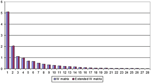
It is worthwhile to note that the first columns of matrices V and corresponding to the first singular values of these matrices are almost collinear. The angles between the vectors of the first three pairs are 89.95°, 88.92° and 88.08°, respectively. This means that the eigenvectors added to form the extended
matrix are very close to the subspace formed by the main eigenvectors of the W matrix. In accordance with the simplified considerations of the previous section this implies the presence of an error self-compensation effect.
5. Conclusion
A mathematical study of the mechanism of thickness errors correlation by direct BBM has been performed and it was shown that due to this monitoring algorithm the error vector tends to be orthogonal to the main eigenvectors of the matrix W presenting the operation of this mechanism. Prediction of the existence of a strong error self-compensation effect can be made by comparing singular values of the matrix W and extended matrix that also includes the main eigenvectors of the matrix A composed by the second order derivatives of the optimized merit function. All mathematical results of the performed investigation are confirmed by computational experiments with the data obtained for the optical coating deposition problem where a very strong error self-compensation effect has been practically observed.
The presented results pave the way for the pre-production evaluation of direct BBM applicability to the production of challenging types of the modern thin film optical coatings. They make it possible to predict whether this type of production control will provide an essential advantage for manufacturing coatings with superior spectral properties in comparison with other modern production control techniques.
Production control with BBM is in first turn applicable for optical coatings with working spectral ranges in visible and infrared (IR) spectral regions. It is difficult to implement this type of monitoring technique for coatings with spectral characteristics specified in other spectral ranges such as UV, EUV and X-ray spectral ranges. Fortunately coatings of the latter types are typically produced with very stable deposition processes and it is possible to monitor their production by deposition time using well-calibrated deposition rates. Nowadays the main challenge is the reliable control of complicated optical coatings for visible and IR spectral ranges and we hope that the presented results will meet growing demands for a better production control in these ranges.
Acknowledgements
The authors express their gratitude to Academician Eugene Tyrtyshnikov for his advices concerning mathematical aspects of this work and to Dr Michael Trubetskov for many valuable comments related to the content of this work.
Disclosure statement
No potential conflict of interest was reported by the authors.
Funding
The work was supported by the Russian Science Foundation [grant number 16-11-10219].
References
- Kaiser N, Pulker HK. Optical interference coatings. Springer series in optical sciences. Berlin-Heidelberg: Springer-Verlag; 2003.10.1007/978-3-540-36386-6
- Piegari A, Flory F, editors. Optical thin films and coatings: from materials to applications. Woodhead publishing series in electronic and optical materials. Cambridge: Woodhead; 2013.
- Tikhonravov AV, Trubetskov MK. Modern design tools and a new paradigm in optical coating design. Appl Opt. 2012;51:7319–7332.10.1364/AO.51.007319
- Furman Sh, Tikhonravov A. Basics of optics of multilayer systems. Lausanne: Frontieres; 1992.
- Tikhonravov AV. Synthesis of optical coatings using optimality conditions. Vestnik MGU Phys Astron Ser. 1982;23:91–93.
- Tikhonravov A, Trubetskov M, DeBell G. Application of the needle optimization technique to the design of optical coatings. Appl Opt. 1996;35:5493–5508.10.1364/AO.35.005493
- Tikhonravov A, Trubetskov M, DeBell G. Optical coating design approaches based on the needle optimization technique. Appl Opt. 2007;46:704–710.10.1364/AO.46.000704
- Tikhonravov A, Trubetskov M, Amotchkina T. Optical monitoring strategies. In: Piegari A, Flory F, editors. Optical thin films and coatings: from materials to application. Cambridge: Woodhead; 2013. p. 62–93.10.1533/9780857097316.1.62
- Tikhonravov AV, Trubetskov MK. Automated design and sensitivity analysis of wavelengh-division multiplexing filters. Appl Opt. 2002;41:3176–3182.10.1364/AO.41.003176
- Vidal B, Fornier A, Pelletier E. Optical monitoring of nonquarterwave multilayer filters. Appl Opt. 1978;17:1038–1047.10.1364/AO.17.001038
- Vidal B, Fornier A, Pelletier E. Wideband optical monitoring of nonquarterwave multilayer filters. Appl Opt. 1979;18:3851–3856.10.1364/AO.18.003851
- Vidal B, Pelletier E. Nonquarterwave multilayer filters: optical monitoring with a minicomputer allowing correction of thickness errors. Appl Opt. 1979;18:3857–3862.10.1364/AO.18.003857
- Tikhonravov A, Trubetskov M, Amotchkina T. Investigation of the effect of accumulation of thickness errors in optical coating production by broadband optical monitoring. Appl Opt. 2006;45:7026–7034.10.1364/AO.45.007026
- Tikhonravov A, Trubetskov M, Amotchkina T. Investigation of the error self-compensation effect associated with broadband optical monitoring. Appl Opt. 2011;50(9):C111–C116.10.1364/AO.50.00C111
- Tikhonravov AV, Trubetskov MK. Computational manufacturing as a bridge between design and production. Appl Opt. 2005;44:6877–6884.10.1364/AO.44.006877
- Zhupanov V, Kozlov I, Fedoseev V, et al. Production of Brewster-angle thin film polarizers using ZrO2/SiO2 pair of materials. Appl Opt. 2017;56:C30–4.10.1364/AO.56.000C30
- Stolz CJ. Status of NIF mirror technologies for completion of the NIF facility. Proc SPIE. 2008;7101:710115.10.1117/12.797470
- OptiLayer.com [Internet]. Available from: http://www.optilayer.com
- Tikhonravov AV. Inverse problems in the optics of layered media. Vestnik MGU Comput Math Cybern Ser. 2006;15(3):66–76.
- Tikhonravov AV, Trubetskov MK. Online characterization and reoptimization of optical coatings. In: Amra C, Kaiser N, Macleod HA, editors. Advances in optical thin films. Proceedings of SPIE. Vol. 5250. 2003. p. 406–413.