
 ?Mathematical formulae have been encoded as MathML and are displayed in this HTML version using MathJax in order to improve their display. Uncheck the box to turn MathJax off. This feature requires Javascript. Click on a formula to zoom.
ABSTRACT
Graded permittivity materials have gained significant attention due to their exceptional ability to regulate electric fields. Multi-material stereolithography (SLA) 3D printing has opened up new possibilities for creating such materials. However, conventional SLA printers typically generate graded material using fixed printing parameters and multiple feedstocks with limited differences, resulting in a constrained capacity for modulating the electric field distribution. To address this limitation, we have developed a multi-material, parameter-controllable SLA strategy, enabling us to assign varying printing parameters for each building layer and switch between feedstocks with significant differences. Solid insulators with graded permittivity are optimised through electric field distribution simulations and subsequently manufactured using our innovative multi-material SLA approach. A 4-layered graded insulator effectively decreases the maximum electric field strength from 82.5–30.8 kV/mm. Both flashover tests and partial discharge signals confirm that graded insulators outperform homogeneous ones in electrical insulation.
1. Introduction
Solid insulators are commonly used as electrical components to provide mechanical support and separate conductors [Citation1]. However, in high voltage applications such as aerospace, military, and power grid transmission [Citation2–4], the electric field distribution on the surface of solid insulators tends to be highly non-uniform. Especially, the maximum electric field strength (Emax) generated at the triple junction can lead to charge accumulation or partial discharge [Citation5,Citation6].
Based on the target of relaxing the electric field concentration, approaches including using corona rings, redesigning conductor shapes, or optimising insulator structures have been developed to modulate the electric field distribution in electrical devices [Citation7–10]. Nevertheless, these conventional methods have increased structural complexity and manufacturing costs. In recent years, a novel concept involving graded permittivity insulators has emerged due to their remarkable electric field relaxation effect in high voltage applications [Citation1,Citation2,Citation11–14]. For instance, researchers have employed techniques like centrifugation, mixture casting, surface modification, and hot-pressing to create non-linear or graded permittivity insulators, effectively reducing high electric field strengths at critical points [Citation2,Citation15–25]. However, these methods fall short in manufacturing complex structures (e.g. hollow structures) and typically exhibit low processing efficiency. The application of 3D printing has created new possibilities for fabricating solid insulators with graded permittivity [Citation26–31]. Among different 3D printing technologies, SLA stands out because it achieves an excellent balance between printing speed and precision [Citation28,Citation32,Citation33]. Here, the graded materials can be in-situ synthesised layer by layer (the so-called multi-material SLA), providing precise control over the material composition of each layer [Citation34,Citation35].
Multi-material SLA 3D printing has found extensive use in the fabrication of graded materials [Citation28,Citation36–38]. However, a challenge in the field of multi-material SLA remains the development of novel strategies that can control printing parameters (exposure time and preset layer height) for every printing layer because most commercial SLA printers typically use a uniform set of parameters throughout the entire printing process, with no provision for parameter adjustments during printing [Citation39]. Multi-material SLA, which involves different formulations, often requires longer exposure times and smaller layer heights when printing with scattering formulations that contain high permittivity fillers; conversely, a faster exposure process can be applied when creating parts using pure liquid resin or refractive index-matching suspensions [Citation40]. The ability to achieve flexible, layer-level digital control over exposure time and layer height to accommodate a range of materials can significantly enhance the fabrication speed and increase the versatility of multi-material 3D printing.
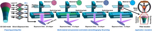
Herein, we develop a multi-material and parameter-controllable SLA strategy to manufacture graded permittivity composites for high voltage insulators (). To modify the material's permittivity, we have blended epoxy resin with BaTiO3, a dielectric ceramic commonly used in electrical insulation due to its high permittivity (>2000 at low frequencies <1 kHz) [Citation41,Citation42]. With this digital manufacturing strategy, we have achieved rapid and robust production of graded permittivity composites by employing different resin formulations (filled with varying amounts of BaTiO3) and applying layer-level digital control over exposure time and layer height. This process involves the preparation of printing files (slicing the 3D model into 2D patterns and assigning exposure times per layer) and multi-material SLA 3D printing (switching between different photocurable feedstocks). As a proof of concept, we have manufactured various insulators with graded permittivity based on the electric field simulation analysis.
Figure 1. Multi-material and parameter-controllable SLA 3D printing of high voltage insulators. The process flow consists of preparing printing files (slicing the 3D model into 2D patterns and assigning exposure times per layer) and multi-material SLA 3D printing (switching between different photocurable feedstocks). The slice numbers and exposure times are indicative only. Formulations filled with different amounts of BaTiO3 particles are used to modulate the resin properties, resulting in a composite print with a gradient in permittivity (right panel).
2. Materials and methods
An epoxy-acrylate-based resin (Esun3d Tech., Shenzhen, China) has been used as the matrix, which is sensitive to 405 nm light [Citation40,Citation43]. Commercially available BaTiO3 particles (Aladdin Chemicals, Shanghai, China) were employed as fillers. The morphology of BaTO3 particles was taken by an S-4800 scanning electron microscope (HITACHI, Japan), while the particle size distribution was measured with a Malvern Zetasizer Nano ZS90 (Malvern Panalytical Ltd., UK). BYK dispersant (BYK-9076, BYK Chemie, Germany; further referred to as ‘BYK’) served as the surfactant for the particles. Composite feedstocks were formulated by mixing Esun resin with BaTiO3 powders, followed by stirring at 800 rpm for 3 h at room temperature. The mixture was then degassed in a vacuum oven (20 mbar, room temperature) for 30 min. Subsequently, we measured the viscosity using a Brookfield viscometer (NDJ-1, LICHEN Tech., China) with the No. 4 spindle at a spinning rate of n = 12 rpm.
Electric field analysis and simulation were carried out based on a simplified model of a high voltage insulator. This simulation model includes high- and low-voltage electrodes, a cone-type insulator, SF6 gas, and triple junctions on the insulator's surface. The simulation was based on material permittivity at 50 Hz, following IEC 62196–1 and IEC 60195:1965 standards. To ensure accuracy, we employed a high-resolution grid composed of triangular cells to define spatial sampling in the finite element model (FEM). In particular, we utilised the smallest mesh size, approximately 1 μm, around the triple junctions for the electric field analysis.
Before 3D printing, we exposed the feedstocks on a transparent substrate to a known dose of light and measured the resulting cured height using a digital gauge (Awt-chy01, EVERTE Ltd., China). This process provided us with photopolymerization information and working curves for different formulations. We developed a custom SLA printing system that enables a multi-material 3D printing strategy, allowing us to assign different exposure times and layer height presets for each building layer. In our setup, the light source had a wavelength of 405 nm and an irradiation intensity of 2.5 mW/cm2. The projection area was approximately 130 mm × 80 mm, resulting in a pixel size of around 50 μm × 50 μm. Before manufacturing graded permittivity composites, we prepared different formulations with varying BaTiO3 loadings. Multi-material SLA was achieved by mechanically switching the resin tank as the platform ascended. In the printing file, different building parameters (exposure time and preset layer height) were designed to accommodate different formulations. Besides, we incorporated an extra residence time for switching tanks after the platform ascended. Before printing a new material, we cleaned the existing cured SLA parts with ethanol.
The relative permittivity () and dielectric loss (
) of cured samples (2 cm in diameter and 0.5 mm in thickness) with different BaTiO3 ratios were measured using a dielectric impedance-thermal excitation current integrated analyzer (Concept 40, Novocontrol, Germany). The frequency dependence of the
and
was tested from 10 Hz to 1 MHz at room temperature [Citation44]. Flashover tests were conducted using a digitally controlled 100 kV non-PD (partial discharge) power supply (YUTW-10/100, Huasheng Tech., China). The voltage rise rate and discharge time interval were set to 0.2 kV/s and 180 s, respectively.
A modular partial discharge detector (DDX 9121b, HAEFELY HIPOTRONICS, Switzerland) equipped with an AKV 9310 measuring impedance was used to capture the discharge pulse and spectrum. The partial discharge detector included digital filters that enabled us to shift the measurement frequency band into a less noisy range and suppress frequency-dependent noise, thereby enhancing sensitivity.
3. Results and discussion
3.1. Formulation and photopolymerization of BaTiO3-resin suspensions
To improve the electrical properties of the pure resin, BaTiO3 has been introduced to the photocurable resin because of its high [Citation45]. Multi-sized BaTiO3 particles (a-b, 300–700 nm with a d50 = 450 nm) enable the formulation of stable and well-dispersed composite inks [Citation46]. Since SLA is a light-based technique, we had to address the strong scattering caused by the refractive index mismatch between BaTiO3 particles (2.6) and the resin (1.5). Based on the modified Lambert–Beer law and scattering model [Citation40], we mitigated this scattering effect by reducing the ceramic concentration in the resin matrix. Apart from photopolymerization, ceramic fillers typically increase the viscosity of the suspension, leading to poor processibility [Citation40,Citation43]. We formulated a series of composite feedstocks to strike a balance between insulation performance and processability. These feedstocks were created by mixing Esun resin with BaTiO3 particles at 10, 20, 30, 40, and 50 wt% concentrations.
Figure 2. Formulation and photopolymerization of BaTiO3-resin suspensions. (a) Morphology of BaTO3 particles. (b) Particle size distribution of BaTiO3. (c) The viscosity of BaTiO3-resin suspensions. (d) SLA working curves, plotted with different measured cure depths.
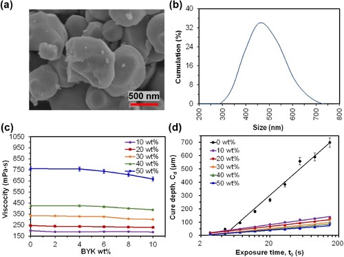
The viscosity increases from around 200–760 mPa·s as the BaTiO3 particle loading increases from 0 to 50 wt% (c). BYK dispersant has been used to formulate suspensions with stable particle dispersion through steric stabilisation [Citation43,Citation45,Citation47]. Several experiments have shown that the optimal BYK content usually falls between 3 and 7 wt% [Citation31,Citation45,Citation48–51]. In this study, we expanded the range to 0-10 wt% to investigate the rheology of the printing suspensions. The viscosity was stable in suspensions with 4–8 wt% BYK content (C).
When BaTiO3 particles are present in the feedstock, the incident light is absorbed by the photoinitiators and scattered by the BaTiO3 particles due to the refractive index mismatch with the resin matrix. As a result, the cure depth () decreases with increasing solid loading (d, cure depth: pure resin > 10 wt% > 20 wt% > 30 wt% > 40 wt% > 50 wt%). For instance, at an exposure time (
) of 150 s, the
decreases from 700 (pure resin) to 70 μm (50 wt% BaTiO3-resin suspension). Based on Jacob's working curve equation [Citation52], the reduction in cure depth by strongly scattering fillers can be offset by prolonging the exposure time (
). Since light energy is the product of
(
is light intensity), increasing the exposure time effectively boosts the exposure energy, thereby increasing the cure depth. For instance, to achieve a cured height of 50 μm, the required exposure times for different suspensions are as follows: 6 s (pure resin), 8 s (10 wt%), 12 s (20 wt%), 20 s (30 wt%), 38 s (40 wt%), and 60 s (50 wt%).
(1)
(1) where
(the cure depth) is linearly proportional to the logarithm of
(the incident light energy),
is the penetration depth related only to the properties of the printing materials and
is the critical energy of light curing (the minimum exposure energy required to initiate polymerisation).
3.2. Electrical properties of BaTiO3-resin composites
The electrical properties of different 3D-printed BaTiO3-resin composites were studied, including the relative permittivity (), the dielectric loss (
), and the flashover properties. Compared to pure resin, the
of BaTiO3-resin composites increases with the BaTiO3 concentration (a-b). For example, at 50 Hz, the
of 50 wt% BaTiO3-resin composite reaches 26.5, approximately six times that of pure resin (around 4.5). Similarly, the
of BaTiO3-resin composites increases with the BaTiO3 concentration (c), which is caused by the substantial differences in dielectric properties (polarizability and conductivity) between the filler and matrix [Citation53,Citation54]. It's worth noting that due to adequate polarisation [Citation55], the
and
are relatively high at low frequency (
kHz). Subsequently, we conducted flashover tests at varying air pressures (ranging from 0.1–0.3 MPa). The flashover voltage does not exhibit significant variation with changes in BaTiO3 concentration. However, it increases from approximately 11–20 kV as the air pressure rises from 0.1–0.3 MPa (d).
Figure 3. Electrical properties of BaTiO3-resin composites. (a) Frequency dependence of permittivity. (b) Permittivity of BaTiO3-resin composites at 50 Hz (experiment and prediction value): the prediction model is the Lichtenecker logarithmic law of mixing [Citation56]. (c) Frequency dependence of dielectric loss. (d) Flashover voltage of BaTiO3-resin composites at different air pressures (0.1–0.3 MPa).
![Figure 3. Electrical properties of BaTiO3-resin composites. (a) Frequency dependence of permittivity. (b) Permittivity of BaTiO3-resin composites at 50 Hz (experiment and prediction value): the prediction model is the Lichtenecker logarithmic law of mixing [Citation56]. (c) Frequency dependence of dielectric loss. (d) Flashover voltage of BaTiO3-resin composites at different air pressures (0.1–0.3 MPa).](/cms/asset/0d48f822-7ab2-435d-99f5-2e9ca6211c3d/nvpp_a_2271447_f0003_oc.jpg)
3.3. Simulation of the electric field distribution in different insulators
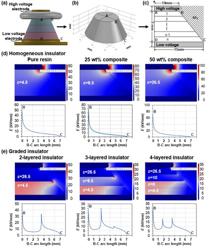
A simplified simulation model of a graded insulator is shown in a-c. In the case of homogeneous insulators (pure resin and 25, 50 wt% BaTiO3-resin composites), the electric field strength (E) decreases from point B (high voltage electrode) to C (low voltage electrode). However, for graded insulators with 2, 3, or 4 layers, the descending curve exhibits multiple convex values at the interfaces between materials with different permittivity (d). We optimised the permittivity values of the multi-layers in graded insulators, simulating values ranging from 4.5–30 with an increment of 0.5. For example, in the case of the 3-layered insulator, the optimal permittivity for the middle layer is 8.5. In the 4-layered insulator, the optimal combination ranges from 26.5–10, 6, and 4.5 (from point B to point C). The maximum electric field strength (Emax) generated in electrical insulating components is critical, as it is linked to partial discharge or charge accumulation issues. In this study, Emax at the triple junction decreased from 82.5–30.8 kV/mm when transitioning from a composite filled with 50 wt% BaTiO3 to the 4-layered graded permittivity composite.
Figure 4. Simulation of the electric field distribution in different insulators. (a-c) Simplified simulation model of a graded insulator. (d-e) Electric field distribution in different insulators. (d) For the homogeneous insulators, the permittivity value is set to 4.5, 8.5 and 26.5 (the measurement value of pure resin and composites at 50 Hz). (e) For the graded insulators, the permittivity value of the multi-layers is optimised by simulating different values ranging from 4.5–30 (with an increment of 0.5).
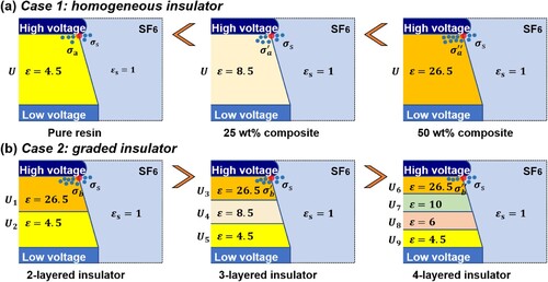
The Emax generated at the triple junction (high voltage conductor – insulator – SF6 gas; red points in a, b) directly depends on the applied voltage and the surface charge density mismatch between the insulator and SF6 gas. To understand the mechanism behind Emax generation, we have to consider two scenarios: homogeneous insulators (a) and graded insulators (b). In the case of homogeneous insulators, where the insulators with the same applied voltage (), the insulator surface charge density increases (
) as the permittivity rises from 4.5–26.5. Consequently, Emax increases when transitioning from pure resin to BaTiO3-filled composite (pure resin < 25 wt% BaTiO3 < 50 wt% BaTiO3). For graded insulators, as we increase the types of heterogeneous materials (from 2 to 4), the voltage decreases (
) because the graded materials can uniform the voltage distribution. This voltage distribution further leads to a decrease in surface charge density (
). As a result, Emax decreases when transitioning from 2-layered to 4-layered insulators (4-layered < 3-layered < 2-layered). In direct comparisons between graded and homogeneous insulators, graded permittivity materials consistently yield lower Emax values due to their ability to uniform voltage distribution.
Figure 5. The generation mechanism of maximum electric field strength (Emax) at the triple junction. (a) Homogeneous insulators. (b) Graded insulators.
3.4. Multi-material SLA of graded insulators and their electrical properties
We successfully fabricated insulators with graded permittivity using multi-material SLA 3D printing technology based on the simulation results. As an illustrative example, we simulated the optimal permittivity combination for the 4-layered insulator: 26.5-10-6-4.5 (d), which combination corresponds to composites filled with 0, 13, 33, and 50 wt% BaTiO3 (b). For different BaTiO3-filled suspensions, the reduction in cure depth by strong scattering can be offset by either prolonging the exposure time or reducing the layer height [Citation42,Citation57]. Conversely, pure resin enables acceleration of the build process as it can be cured with a short exposure time. As a result, we designed dynamic digital exposure strategies for different suspensions and insulators (). Taking the 3-layered insulator as an example (a), different printing parameters were designed for different formulations: Material A (Pure resin) – layer height: 50 µm/layer, exposure time: 6 s/layer; Material B (Composite filled with 25 wt% BaTiO3) – layer height: 10 µm/layer, exposure time: 16 s/layer; Material C (Composite filled with 50 wt% BaTiO3) – layer height: 10 µm/layer, exposure time: 30 s/layer.
Figure 6. Multi-material SLA of different insulators and their flashover properties. (a) 3D printing process flow (an example of the 3-layered insulator). (b) 3D-printed insulators. (c-d) Flashover properties of different insulators at different air pressures (air: 0.1–0.4; SF6: 0.05–0.3).
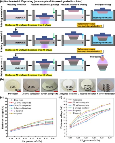
Table 1. Printing parameters for different suspensions and graded insulators.
Using different formulations and building parameters, we printed different insulators (b). After the 3D-printed insulators were post-cured and dried, flashover tests were conducted to evaluate their insulation performance. The flashover voltage was found to increase as air/SF6 pressure increased. It's worth noting that the flashover voltage is higher in the SF6 condition than in the air (c-d), indicating that the 3D-printed insulators operate better in the SF6 condition. By optimising dielectric parameters and using gradient materials, the electric field distribution at the gas–solid interface becomes more uniform. As a result, graded insulators exhibit enhanced flashover properties, enabling discharge to occur at higher voltages. The performance of different insulators is similar to the simulation results, where the 4-layered and 3-layered graded insulators outperform the 2-layered graded insulators and pure resin insulators. Conversely, the insulator with a composite filled with 50 wt% BaTiO3 performs the poorest.
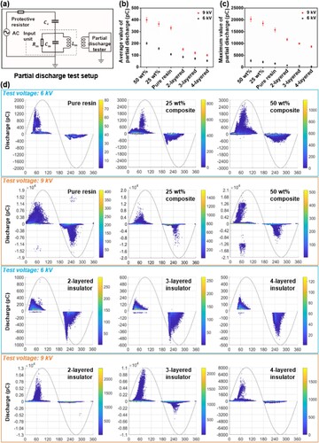
When high voltages are applied, the high electric field generated in the electrical insulating components might cause partial discharge or sudden electrical breakdown [Citation58,Citation59]. In this study, we collected partial discharge signals from various insulator samples tested at 6 and 9 kV with a frequency of 50 Hz. Compared to the homogeneous insulators (pure resin and composite filled with BaTiO3), graded insulators exhibited a reduction in the amplitude of partial discharge, resulting in improved performance in terms of average and maximum partial discharge values (). Regarding the performance of graded insulators, it's worth noting that the 4-layered insulator does not demonstrate a significant advantage over the 2-layered or 3-layered insulator. For instance, at a test voltage of 9 kV, the maximum partial discharge values for different graded insulators were as follows: 10697 pC (2-layered), 9975 pC (3-layered), and 8895 pC (4-layered). Similarly, the average partial discharge values for these graded insulators were 150 pC (2-layered), 125 pC (3-layered), and 100 pC (4-layered). These insights inform the design and manufacturing of graded insulators, helping to strike a balance between the final device's functionality and the complexity of the manufacturing process.
Figure 7. Partial discharge tests for different insulators. (a) Partial discharge test setup. (b) Average and (c) maximum values of partial discharge. (d) Partial discharge signals of the samples at different voltages (6 and 9 kV with a frequency of 50 Hz).
3.5. Benchmark study and perspectives
Various technologies have been employed to fabricate graded permittivity composites. Notably, methods such as flexible mixture casting, surface modification, hot-pressing, and 3D printing have shown significant potential in modulating electric field distribution and improving surface flashover performance (). The multi-material SLA 3D-printed graded permittivity composite shows good electrical performance comparable to other methods. Most techniques reduce the maximum electric field by >50% and increase the flashover voltage by >40%. In comparison to casting and surface modification, 3D printing methods, especially fused deposition modelling (FDM) and SLA, have emerged as promising alternatives for crafting graded permittivity materials due to the high degree of design freedom and highly efficient production. Specifically, SLA stands out when high-resolution and filled feedstock is required.
Table 2. Comparison of different insulation materials/structures.
Theoretically, the present multi-material SLA technique can allocate distinct material compositions for each printed layer, potentially achieving a continuous gradient in BaTiO3 content ranging from 0% to 50 wt%. However, pursuing this approach is deemed unnecessary as the 4-layered insulator in this study does not exhibit a significant advantage over the 3-layered insulator regarding flashover and partial discharge properties. When evaluating the marginal improvement in performance against the drawbacks – such as prolonged building time and heightened manufacturing complexity due to formulating multiple feedstocks before printing and increasing waiting times during tank switching – a more prudent strategy would involve designing and fabricating materials with suitable gradient levels tailored to specific applications rather than pursuing continuous graded permittivity materials.
4. Conclusion
A multi-material and parameter-controllable SLA 3D printing strategy that can assign different exposure times and layer height presets for each building layer is developed to fabricate graded permittivity composites for high voltage insulators. The 3D-printed graded insulators outperform homogeneous ones, as confirmed through simulations, flashover tests, and partial discharge signals. When considering the balance between device functionality and manufacturing complexity, it becomes clear that designing insulators with tailored gradient levels for specific applications is a more practical approach than pursuing continuously graded insulators. For instance, our study highlights the effectiveness of 4-layered/3-layered graded insulators in manipulating electric field distribution and enhancing surface flashover performance. Beyond high voltage insulators, the multi-material and parameter-controllable SLA strategy developed here holds significant potential for precision packaging in microelectronics.
CRediT authorship contribution statement
Lipeng Zhong: Conceptualization, Methodology, Writing – original draft.
Juxian Du: Investigation, Methodology, Data curation.
Yingwei Xi: Investigation, Methodology, Data curation.
Feng Wang: Investigation, Methodology.
Linmei Wu: Analysis.
Jinyu Li: Investigation, Methodology.
Min Tu: Analysis, Writing – review & editing.
Xiaopeng Li: Analysis, Writing – review & editing.
Guanghai Fei: Conceptualization, Analysis, Writing – original draft, review, editing.
Disclosure statement
No potential conflict of interest was reported by the author(s).
Additional information
Funding
References
- Li J, Liang H, Chen Y, et al. Promising functional graded materials for compact gaseous insulated switchgears/pipelines. High Voltage. 2020;5(3):231–240. doi:10.1049/hve.2019.0327
- Rachmawati HK, Kato K, Zebouchi N, et al. Electric field grading and discharge inception voltage improvement on HVDC GIS/GIL spacer with permittivity and conductivity graded materials (ϵ / σ -FGM). IEEE Trans Dielectr Electr Insul. 2022;29(5):1811–1817. doi:10.1109/TDEI.2022.3194489
- Luo Y, Tang J, Pan C, et al. Dynamics of surface charge and electric field distributions on basin-type insulator in GIS/GIL Due to voltage polarity reversal. High Voltage. 2020;5(2):151–159. doi:10.1049/hve.2019.0217
- Fuertes V, Cabrera MJ, Seores J, et al. Hierarchical micro-nanostructured albite-based glass-ceramic for high dielectric strength insulators. J Eur Ceram Soc. 2018;38(7):2759–2766. doi:10.1016/j.jeurceramsoc.2018.02.009
- Li C, Hu J, Lin C, et al. The potentially neglected culprit of DC surface flashover: electron migration under temperature gradients. Sci Rep. 2017;7(1):3271. doi:10.1038/s41598-017-03657-1
- Yang X, Zhao X, Hu J, et al. Grading electric field in high voltage insulation using composite materials. IEEE Electr Insul Mag. 2018;34(1):15–25. doi:10.1109/MEI.2018.8246118
- Dominguez DC, Espino-Cortes FP, Gomez P. Optimization of electric field grading systems in non-ceramic insulators. In: 2011 Electrical Insulation Conference (EIC); IEEE; 2011. p. 231–234. doi:10.1109/EIC.2011.5996152
- Hussain MK, Alshadeedi BM. Optimal design of high voltage composite insulators with grading rings in different configurations. Electr Power Syst Res. 2023;221(August):109493. doi:10.1016/j.epsr.2023.109493
- Doshi T, Gorur R, Hunt J. Electric field computation of composite line insulators up to 1200 KV AC. IEEE Trans Dielectr Electr Insul. 2011;18(3):861–867. doi:10.1109/TDEI.2011.5931075
- Zhao L, Su J-C, Peng J-C, et al. Design, simulation, and experiments for an improved coaxial high-voltage vacuum insulator in TPG700 for high-power microwave generation. IEEE Trans Electron Devices. 2014;61(6):1883–1889. doi:10.1109/TED.2013.2283748
- Yao H, Du B, Liang H, et al. Electric field relaxation of HVDC GIL spacer with surface conductivity gradient material (σ-SFGM) using electrospinning technology. IEEE Trans Dielectr Electr Insul. 2022;29(3):1167–1174. doi:10.1109/TDEI.2022.3171249
- Kurimoto M, Kato K, Hanai M, et al. Application of functionally graded material for reducing electric field on electrode and spacer interface. IEEE Trans Dielectr Electr Insul. 2010;17(1):256–263. doi:10.1109/TDEI.2010.5412025
- Li X-R, Liu Z, Li W-D, et al. 3D printing fabrication of conductivity non-uniform insulator for surface flashover mitigation. IEEE Trans Dielectr Electr Insul. 2019;26(4):1172–1180. doi:10.1109/TDEI.2019.007938
- Imai T, Hoshina Y, Kojima H, et al. Resin injection behavior in process of manufacturing insulation spacer with permittivity gradient using computational fluid dynamics. IEEE Trans Dielectr Electr Insul. 2019;26(5):1669–1677. doi:10.1109/TDEI.2019.008239
- Du B, Yao H, Liang H, et al. Multidimensional Functionally Graded Materials (ϵ/σ-MFGM) for HVDC GIL/GIS spacers. IEEE Trans Dielectr Electr Insul. 2022;29(5):1966–1973. doi:10.1109/TDEI.2022.3190810
- Hayakawa N, Miyaji Y, Kojima H, et al. Simulation on discharge inception voltage improvement of GIS spacer with permittivity graded materials (ϵ-FGM) using flexible mixture casting method. IEEE Trans Dielectr Electr Insul. 2018;25(4):1318–1323. doi:10.1109/TDEI.2018.007236
- Hayakawa N, Ishiguro J, Kojima H, et al. Fabrication and simulation of permittivity graded materials for electric field grading of gas insulated power apparatus. IEEE Trans Dielectr Electr Insul. 2016;23(1):547–554. doi:10.1109/TDEI.2015.005237
- Shumiya H, Kato K, Okubo H. Fabrication and prediction techniques for FGM (Functionally Graded Materials) application to solid insulators. In: CEIDP ‘05. 2005 Annual Report Conference on Electrical Insulation and Dielectric Phenomena, 2005., 2005; IEEE. p. 673–676. doi:10.1109/CEIDP.2005.1560772
- Du BX, Liang HC, Li J. Surface coating affecting charge distribution and flashover voltage of cone-type insulator under DC stress. IEEE Trans Dielectr Electr Insul. 2019;26(3):706–713. doi:10.1109/TDEI.2018.007616
- Kong F, Zhao M, Zhang C, et al. Two-phase-interfaced, graded-permittivity titania electrical insulation by atmospheric pressure plasmas. ACS Appl Mater Interfaces. 2022;14(1):1900–1909. doi:10.1021/acsami.1c18044
- Yu W, Kong F, Dong P, et al. Depositing chromium oxide film on alumina ceramics enhances the surface flashover performance in vacuum via PECVD. Surf Coat Technol. 2021;405(January):126509. doi:10.1016/j.surfcoat.2020.126509
- Sun X-L, Xun T, Zhong H-H, et al. Improved Surface flashover characteristics of ceramic vacuum interface by surface treatment. In 2018 28th International Symposium on Discharges and Electrical Insulation in Vacuum (ISDEIV), 1:151–154. IEEE, 2018. doi:10.1109/DEIV.2018.8537070
- Du BX, Wang ZH, Li J, et al. Epoxy insulator with surface graded-permittivity by magnetron sputtering for gas-insulated line. IEEE Trans Dielectr Electr Insul. 2020;27(1):197–205. doi:10.1109/TDEI.2019.008385
- Li S. Improvement of surface flashover in vacuum. High Voltage. 2020;5(2):122–133. doi:10.1049/hve.2020.0021
- Li S, Huang Q, Zhang T, et al. New organic insulation system to improve the surface-flashover characteristics in vacuum. IEEE Trans Plasma Sci. 2010;38(12):3434–3441. doi:10.1109/TPS.2010.2080288
- Belen A, Güneş F, Mahouti P, et al. A novel design of high performance multilayered cylindrical dielectric lens antenna using 3D printing technology. Int J RF Microwave Comput Aided Eng. 2020;30(1):e21988. doi:10.1002/mmce.21988
- Phatharapeetranun N, Ksapabutr B, Marani D, et al. 3D-Printed barium titanate/poly-(vinylidene fluoride) nano-hybrids with anisotropic dielectric properties. J Mater Chem C. 2017;5(47):12430–12440. doi:10.1039/C7TC03697C
- Kurimoto M, Sawada T, Kato T, et al. 3D printing of 2 layered permittivity-graded material using UV-cured-resin/alumina composite. In: 2018 12th International Conference on the Properties and Applications of Dielectric Materials (ICPADM), 2018-May; IEEE, 2018. p. 1010–1013. doi:10.1109/ICPADM.2018.8401209
- Diaham S, Valdez Nava Z, Leveque L, et al. An original in-situ way to build Field Grading Materials (FGM) with permittivity gradient using electrophoresis. In: 2018 IEEE 2nd International Conference on Dielectrics (ICD), IEEE, 2018. p. 1–4. doi:10.1109/ICD.2018.8514572
- Nardi T, Mora N, Rachidi F, et al. Graded-permittivity polymer nanocomposites as superior dielectrics. Compos Sci Technol. 2016;129(June):1–9. doi:10.1016/j.compscitech.2016.04.010
- Zhong L, Liu W, Sun Y, et al. Electrically assisted stereolithography 3D printing of graded permittivity composites for in-situ encapsulation of Insulated Gate Bipolar Transistors (IGBTs). Mater Des. 2023;233(September):112220. doi:10.1016/j.matdes.2023.112220
- Ligon SC, Liska R, Stampfl J, et al. Polymers for 3D printing and customized additive manufacturing. Chem Rev. 2017;117(15):10212–10290. doi:10.1021/acs.chemrev.7b00074
- Ge Q, Li Z, Wang Z, et al. Projection micro stereolithography based 3D printing and Its applications. Int J Extreme Manuf. 2020;2(2):022004. doi:10.1088/2631-7990/ab8d9a
- Wicker RB, MacDonald EW. Multi-material, multi-technology stereolithography: this feature article covers a decade of research into tackling one of the major challenges of the stereolithography technique, which Is including multiple materials in One construct. Virtual Phys Prototyp. 2012;7(3):181–194. doi:10.1080/17452759.2012.721119
- Vaezi M, Chianrabutra S, Mellor B, et al. Multiple material additive manufacturing – part 1: a review. Virtual Phys Prototyp. 2013;8(1):19–50. doi:10.1080/17452759.2013.778175
- Sampson KL, Deore B, Go A, et al. Multimaterial vat polymerization additive manufacturing. ACS Appl Polym Mater. 2021;3(9):4304–4324. doi:10.1021/acsapm.1c00262
- Ravanbakhsh H, Karamzadeh V, Bao G, et al. Emerging technologies in multi-material bioprinting. Adv Mater. 2021;33(49):2104730. doi:10.1002/adma.202104730
- Rafiee M, Farahani RD, Therriault D. Multi-material 3D and 4D printing: a survey. Adv Sci. 2020;7(12):1902307. doi:10.1002/advs.201902307
- Fei G, Parra-Cabrera C, Li Y, et al. Stereolithographic 3D printing of graded porous materials via an integrated digital exposure and selective dissolution strategy. Cell Reports Phys Sci. 2023;4(7):101504. doi:10.1016/j.xcrp.2023.101504
- Fei G, Parra-Cabrera C, Zhong K, et al. Scattering model for composite stereolithography to enable resin–filler selection and cure depth control. ACS Appl Polym Mater. 2021;3(12):6705–6712. doi:10.1021/acsapm.1c01519
- Wang W, Sun J, Guo B, et al. Fabrication of piezoelectric nano-ceramics via stereolithography of low viscous and non-aqueous suspensions. J Eur Ceram Soc. 2020;40(3):682–688. doi:10.1016/j.jeurceramsoc.2019.10.033
- Li W-D, Wang C, Jiang Z-H, et al. Stereolithography based additive manufacturing of high-k polymer matrix composites facilitated by thermal plasma processed barium titanate microspheres. Mater Des. 2020;192(July):108733. doi:10.1016/j.matdes.2020.108733
- Fei G, Nie L, Zhong L, et al. Photocurable resin-silica composites with low thermal expansion for 3D printing microfluidic components onto printed circuit boards. Mater Today Commun. 2022;31(June):103482. doi:10.1016/j.mtcomm.2022.103482
- Du J, Tang B, Liu W, et al. Effects of annealing and firing in wet hydrogen on the dielectric breakdown strengths of alumina ceramics. J Adv Ceram. 2020;9(2):173–182. doi:10.1007/s40145-019-0357-x
- Zhong L, Liu W, Xi Y, et al. An integrated structure–material optimization strategy for the packaging of high-voltage insulated gate bipolar transistors. IEEE Trans Dielectr Electr Insul. 2022;29(6):2163–2170. doi:10.1109/TDEI.2022.3211225
- Song SY, Park MS, Lee D, et al. Optimization and characterization of high-viscosity ZrO2 ceramic nanocomposite resins for supportless stereolithography. Mater Des. 2019;180(October):107960. doi:10.1016/j.matdes.2019.107960
- Hoffmann R, Kelly E, Büscher J. Additives for emulsions and dispersions in flexible foam formulations. In: Polyurethanes 2007 Technical Conference; 2007. p. 1–7.
- Fei G, Wei T, Shi Q, et al. Preliminary Study on Hybrid Manufacturing of the Electronic-Mechanical Integrated Systems (EMIS) via the LCD Stereolithography Technology. In: Solid Freeform Fabrication 2019: Proceedings of the 30th Annual International Solid Freeform Fabrication Symposium, 2019. p. 2028–2036. doi:10.26153/tsw/17456
- Sun J, Binner J, Bai J. Effect of surface treatment on the dispersion of nano zirconia particles in non-aqueous suspensions for stereolithography. J Eur Ceram Soc. 2019;39(4):1660–1667. doi:10.1016/j.jeurceramsoc.2018.10.024
- UIIah I, Cao L, Cui W, et al. Stereolithography printing of bone scaffolds using biofunctional calcium phosphate nanoparticles. J Mater Sci Technol. 2021;88(October):99–108. doi:10.1016/j.jmst.2021.01.062
- Chung K, Nenov NS, Park S, et al. Design of optimal organic materials system for ceramic suspension-based additive manufacturing. Adv Eng Mater. 2019;21(10):1900445. doi:10.1002/adem.201900445
- Jacobs PF. Rapid prototyping & manufacturing: fundamentals of stereolithography. society of manufacturing engineers. Dearborn (MI): Society of Manufacturing Engineers; 1992.
- Pan Z, Yao L, Zhai J, et al. Significantly improved dielectric properties and energy density of polymer nanocomposites via small loaded of BaTiO3 nanotubes. Compos Sci Technol. 2017;147(July):30–38. doi:10.1016/j.compscitech.2017.05.004
- İnal M. Determination of dielectric properties of insulator materials by means of ANFIS: a comparative study. J Mater Process Technol. 2008;195(1–3):34–43. doi:10.1016/j.jmatprotec.2007.04.106
- Samet M, Levchenko V, Boiteux G, et al. Electrode polarization vs. Maxwell-Wagner-Sillars interfacial polarization in dielectric spectra of materials: characteristic frequencies and scaling laws. J Chem Phys. 2015;142(19). doi:10.1063/1.4919877
- Cho S-D, Lee S-Y, Hyun J-G, et al. Comparison of theoretical predictions and experimental values of the dielectric constant of Epoxy/BaTiO3 composite embedded capacitor films. J Mater Sci: Mater Electron. 2005;16(2):77–84. doi:10.1007/s10854-005-6454-3
- Wu X, Lian Q, Li D, et al. Effects of soft-start exposure on the curing characteristics and flexural strength in ceramic projection stereolithography process. J Eur Ceram Soc. 2019;39(13):3788–3796. doi:10.1016/j.jeurceramsoc.2019.05.004
- Zhang B, Ghassemi M, Zhang Y. Insulation materials and systems for power electronics modules: a review identifying challenges and future research needs. IEEE Trans Dielectr Electr Insul. 2021;28(1):290–302. doi:10.1109/TDEI.2020.009041
- Ullah R, Akbar M. Effect of AC stressed aging on partial discharge, thermal and tensile performance of silicone rubber-based composites. Compos Commun. 2021;24(April):100634. doi:10.1016/j.coco.2021.100634
- Li W-D, Zhao J-W, Chen Y, et al. Surface insulation performance of 3D printed functionally graded insulator fabricated by Active-Mixing Fused Deposition Modeling (AM-FDM). In: 2020 IEEE International Conference on High Voltage Engineering and Application (ICHVE). IEEE; 2020. p. 1–4. doi:10.1109/ICHVE49031.2020.9280089
- Veselý P, Froš D, Hudec T, et al. Dielectric spectroscopy of PETG/TiO 2 composite intended for 3D printing. Virtual Phys Prototyp. 2023;18(1). doi:10.1080/17452759.2023.2170253
- Kurimoto M, Ozaki H, Yamashita Y, et al. Dielectric properties and 3d printing of Uv-cured acrylic composite with alumina microfiller. IEEE Trans Dielectr Electr Insul. 2016;23(5):2985–2992. doi:10.1109/TDEI.2016.7736862
- Chen M, Xu M, Li W, et al. Preparation of barium titanate nanowires via electrospinning and the performance in stereolithographic 3D printing nanocomposites. In: 2020 IEEE Conference on Electrical Insulation and Dielectric Phenomena (CEIDP), 2020-Octob; IEEE; 2020. p. 99–102. doi:10.1109/CEIDP49254.2020.9437488
- Yang Y, Chen Z, Song X, et al. Three dimensional printing of high dielectric capacitor using projection based stereolithography method. Nano Energy. 2016;22(April):414–421. doi:10.1016/j.nanoen.2016.02.045
- Wang Q, Liu X, Qiang Z, et al. Cellulose nanocrystal enhanced, high dielectric 3D printing composite resin for energy applications. Compos Sci Technol. 2022;227(August):109601. doi:10.1016/j.compscitech.2022.109601