
ABSTRACT
Locally confined electrodeposition of precursors in liquid is one of the most effective approaches for additive manufacturing of metal microstructures. However, reported data were overwhelmingly obtained at the micrometer scale, whereas sub-microscale and nanoscale microstructures are of interest in electromagnetic or optical fields. In this paper, we propose a cold-constrained local electrodeposition (CCLE) technique to address the issue that locally confined electrodeposition of precursors in liquid is challenging in the fabrication of sub-microscale three-dimensional microstructures. Microstructure printing is conducted via locally confined electrodeposition by a pipette with a sub-microscale opening to deliver electrodeposition electrolyte in a supporting electrolyte. The electrolytes are cooled to 5 °C, which constrains the large-scale diffusion of the electrodeposition electrolyte and significantly reduces the electrodeposition area. It is found that the proposed CCLE technique can print sub-microscale (minimum size is low to 290 nm) structures, which have highly uniform deposits, smooth surfaces and high strength.
1. Introduction
Metals have unique electrical conductivity, mechanical properties, and thermal conductivity, allowing the wide application of metal structures in industry. Additive manufacturing (AM) based on layer-by-layer deposition can remove geometrical constraints of manufacturing for the fabrication of tailored metal structures [Citation1–4]. With advancements in AM, printed metal structures of different scales have been fabricated, such as rocket engines, [Citation5] integrally bladed disks [Citation6] at the macroscale, and optical microdevices [Citation7] and microelectronics devices[Citation8] at the microscale. Macroscale AM has realised its full potential for the fabrication of complex structures with high resolution, but microscale AM faces challenges [Citation9].
For fabricating high-resolution metal microstructures, various novel metal microscale AM techniques have recently been developed, i.e. direct ink writing (DIW), [Citation10,Citation11] electrohydrodynamic printing (EHD), [Citation12,Citation13] and focused electron/ion beam induced deposition (FEBID/FIBID) [Citation14,Citation15]. DIW and EHD rely on metal nanoparticles that are delivered and solidified to form a microstructure with a high resolution. Nevertheless, these two techniques are difficult to prepare metal structures with high strength and conductivity, because nanoparticles are surrounded by a less conductive organic impurity. FEBID/FIBID is based on the beam-induced dissociation of precursor molecules. Although FEBID/FIBID has a high resolution and low fabrication complexity, the metal purity of the prepared microstructures is as low as 10–20 at%, which reduces the strength and conductivity of the metal structures [Citation16]. Metal microstructures are mostly required in the areas of sensors, optics, microelectronics, and microelectromechanical systems, where the strength and conductivity are key parameters. Thus, DIW, EHD, and FEBID/FIBID face a tradeoff between the capacity and the limitations of the metal strength and conductivity.
Electrochemical AM has the same advantages as electrodeposition, i.e. simple metal deposition, an easy control process, and a high metal purity and density. The family of electrochemical AM techniques includes microanode-guided electroplating, [Citation17] meniscus-confined electrodeposition (MCED),[Citation18] locally confined deposition of precursors in liquid (i.e. FluidFM printing, which relies on a scanning ion conductance microscope), [Citation19,Citation20] and electrohydrodynamic redox printing (EHD-RP) [Citation21]. Among these techniques, MCED and EHD-RP have realised printing with impressive nanoscale resolutions by confining the deposition in a nanoscale area, implying that electrochemical AM can target high-resolution printing. However, they are often viewed as limited for the fabrication of complex three-dimensional (3D) structures. In contrast, locally confined deposition of precursors in liquid (mainly the FluidFM technique) is the most advanced method for printing complex designs and was used to print an impressive 1:70000 replica of Michelangelo’s David [Citation22].
The electrochemical AM technology has been developing. At the beginning, it is challenging for EC printing techniques (MCED) to prepare complex microscale structures because the movement of the pipette is restricted during the printing (The pipette shall move very slowly to keep the meniscus unbroken) [Citation23]. Then, with the appearance of the locally confined deposition of precursors in liquid (FluidFM), EC AM can fabricate complex microscale structures because the pipette moves freely, but most efforts so far have been focused on deposition of copper [Citation19,Citation20]. Next, the locally confined deposition of precursors in liquid is extended to printed other metals, such as Ag, Ni, Ni-Mn and Ni-Co [Citation24,Citation25]. Up to now, the technology of the locally confined deposition of precursors in liquid has been shown as the most advanced electrochemical 3D printing technology in terms of printing complex designs. However, it is difficult to achieve a high resolution below the microscale and high printing quality. The challenge is constraining the large-scale diffusion of metal ions in the liquid environment, which increases the deposition area and causes severe stray electrodeposition on the printed surface during the printing (The stray electrodeposition means that metal electrodeposition happens on unwanted areas, that refers to the surface of the already printed structure or the area on the cathode around the printed structure) [Citation9,Citation19,Citation20]. The stray electrodeposition negatively influences the printing quality and resolution.
To address this challenge, we introduce a novel cold-constrained local electrodeposition (CCLE) technique for producing sub-microscale 3D features relying on locally confined deposition of precursors in liquid. During the printing, the supporting electrolyte is cooled to 5 °C, which constrains the large-field diffusion of metal ions and allows a far smaller electrodeposition area. Optimisation of the deposition potentials and pressure for metal-ion delivery allows control of the morphology. The CCLE technique prints 3D sub-microscale microstructures with relatively high uniform deposits and smooth surfaces. This study provides an important direction for locally confined deposition of precursors in liquid to improve printing accuracy and quality, making it possible to prepare high-quality, high-strength and good-conductivity complex 3D structures in the industry.
2. Experimental section
Main settings of experimental conditions were listed in . It included electrolytes, substrate, nanopipette, printing setups and pre-printing tests. The detailed conditions were described as followed.
Table 1. Main experimental conditions.
Electrolyte, Substrate, and Nanopipette: The electrodeposition electrolyte consisted of 0.4 M copper (II) sulphate pentahydrate (CuSO4·5H2O) and 0.6 M sulphuric acid (H2SO4). A sulphuric acid solution (0.0001 M) with a pH of 4 was prepared as the supporting electrolyte. All the electrolytes were prepared using deionised water and filtered through a 0.1-μm PVDF membrane (Millex-VV, MerckMillipore, Germany). A Si substrate (1 × 1 cm2) coated with a 3-nm-thick Ti adhesion layer and sputtered with a 25-nm-thick Au top layer was used as the substrate. The ultrasonic cleaning of the substrate was performed with acetone for 10 min and deionised water for 10 min before printing. Glass nanopipettes (TIP, WPI, USA) with openings of 200 and 500 nm were used to locally deliver the electrodeposition electrolyte in the supporting electrolyte. To prevent impurities from blocking the nanopipette, the electrolytes were filtered by using syringe filters with pore size of 200 nm before the printing.
Printing Setup: A three-electrode cell was utilised for the printing via the CCLE technique. A cleaned Au substrate was used as the working electrode, and a Pt electrode and an Ag/AgCl electrode were used as the counter electrode and quasi-reference counter electrode, respectively. All the electrodes were placed inside a resin homemade chamber and connected to a potentiostat (PalmSens4, PalmSens B. V., The Netherlands). To pre-fill the nanopipette with the electrodeposition electrolyte, an pressure of 1000 mbar was applied using a pressure pump (OB1 Mk3+, Elveflow, France). As soon as the electrolyte was ejected from the nanopipette, the printing cell was manually filled with the supporting electrolyte, and the nanopipette was lowered into the bath. The dimensions of the printing cell were 100 mm × 80 mm × 15 mm. The material of the printing cell was poly(ether-ether-ketone). The cathode was fixed in the centre of the printing cell with 5 mm × 5 mm area exposing for printing. The diameter of the cooling tube was 10 mm, and the linear distance between the printing area and the cooling tube was about 15 mm. The cooling tube was completely submerged in the supporting electrolyte. Before the printing, the supporting electrolyte was cooled for 30 min to ensure the temperature completely decreased to the set point. During the printing process, a refrigeration circulator (PC200-A25, Thermo Fisher Scientific, USA) was used to cool the supporting electrolyte. A three-axis nanometre precision motion platform was employed to move the nanopipette using a printing program written in the C language. The positioning accuracies of x, y and z axis were 50 mm ± 1 μm, 50 mm ± 1 μm and 10 mm ± 0.1 μm.
Pre-printing Tests: A PalmSens4 potentiostat was used to perform electrochemical voltammetric tests for macroscopic tracking of the electrodeposition process from the electrodeposition electrolyte and the supporting electrolyte. The scan rate and range of the linear sweep voltammetry were 0.02 V/s and 0 to –1.2 V, respectively.
SEM, TEM, FIB and In-situ SEM: After printing, all the samples were examined using a scanning electron microscope (Regulus 8200, Hitachi, Japan). The microstructures of the deposits were examined using TEM (JEM-2100F, JEOL, Japan). An FIB-SEM instrument (Helios G4 PFIB, FEI, USA) was used to mill longitudinal and transverse sections of the pillars with a current of 30 pA. The In-situ SEM micro-compression experiments were conducted using the Thermofisher Scios 2 and PicoFemto SFP3 Nanomechanics test systems. In the experiment, a flat diamond indenter with a diameter of 8 μm was used to compress the fabricated Cu micropillars at a constant speed of 40 nm/s.
3. Results and discussion
3.1 3D Printing Principle of CCLE
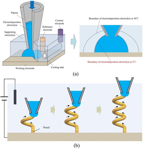
In this study, printing was performed via locally confined electrodeposition by a nanopipette with a sub-microscale opening to deliver the electrodeposition electrolyte (containing metal ions) in the supporting electrolyte (without any metal ions), as shown in (a). The deposition range mainly depends on the diffusion range of the electrodeposition electrolyte in the supporting electrolyte. Large-scale diffusion was not expected. Normally, electrodeposition requires a certain range of metal ion concentration to obtain high-quality metal. Too low ion concentration is easy to cause abnormal metal growth, resulting in lots of defects in the deposits. After the large-scale diffusion, the metal ion concentration around the surface of the already printed structure must be low, easily resulting in abnormal electrodeposition on these surfaces. Therefore, the stray electrodeposition would significantly worsen the electrodeposition localisation and the printing quality. Herein, we propose a CCLE technique. The principle of this technique is that a cooling tube is used to cool the electrolytes during the printing; thus, a low-temperature liquid printing environment is constructed. This is because the cold liquid environment can slow the diffusion of the electrodeposition electrolyte in the supporting electrolyte, [Citation26] which is expected to make as many metal ions as possible electrodeposit on the cathode before the large-scale diffusion. Thus, the CCLE technique is expected to reduce the deposition area, enhance the electrodeposition localisation, limit the stray electrodeposition, and improve the printing quality. After the construction of the cold liquid environment, the structure is printed in a voxel-by-voxel manner, as shown in (b). The voxel electrodeposition position is approached by the nanopipette, and the deposition process is started by delivering the electrodeposition electrolyte and polarising the substrate. Therefore, the trace of the nanopipette defines the shape of the printed structure. During the voxel electrodeposition, the metal grows and eventually touches the nanopipette. Then, the nanopipette must move to the next voxel position quickly for precisely placing all voxels. Here we create a circuit based on a commercial scanning ion-conductance microscope (SICM) [Citation20,Citation27,Citation28]. By identifying and processing this current signal, the system moved the nanopipette to the next printing position in time, allowing voxel-by-voxel printing.
Figure 1. Printing process of CCLE: (a) schematic of CCLE; (b) voxel-by-voxel printing.
3.2 Effects of temperature on diffusion
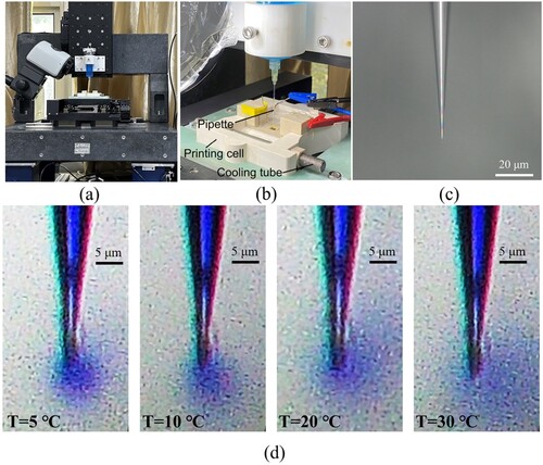
The metal printing was conducted using a custom setup ((a)). The supporting electrolytes were placed in a printing cell ((b)), and the electrodeposition electrolytes were delivered to the supporting electrolytes by a nanopipette with a 500-nm opening ((c)). Before the printing, a microscale diffusion process of the electrodeposition electrolyte in the supporting electrolyte at different temperatures was conducted ((d)), which was used to preliminarily evaluate the effect of the temperature on the diffusion. Here, a 0.4 M CuSO4 solution (with blue pigment added for clear observation) as the electrodeposition electrolyte was added to an H2SO4 solution (∼pH = 4) by using a pressure of 5 mbar for about 2∼3 s. In (d), the blue regions represent the CuSO4 solution, and the other regions represent the H2SO4 solution. As shown, the blue regions became lighter and larger as the temperature increased from 5 to 30 °C. This indicated that the diffusion range of the CuSO4 solution in the H2SO4 solution increased with the temperature. Thus, we drew a preliminary conclusion that the cold liquid environment can reduce the diffusion range of metal ions and significantly reduce the electrodeposition area. This can enhance the electrodeposition localisation and limit the stray electrodeposition. Besides that, the cold liquid environment decreased the diffuse rate of the electrodeposition electrolyte to the surrounding supporting electrolyte. This might maintain the component stability of the electrodeposition electrolyte in the printing area (not only the concentration of metal ions but also the pH). It helped achieve normal metal electrodepositions during the printing.
Figure 2. Microscale diffusion process of the electrodeposition electrolyte in the supporting electrolyte: (a) printing setup; (b) printing cell; (c) nanopipette; (d) diffusion at different temperatures.
Based on the analysis above, it was thought that a lower temperature could obtain a lower diffusion rate of metal ions, resulting in a smaller electrodeposition area in the supporting electrolyte. But the temperature should be above the freezing point of the electrolytes to ensure the printing process could proceed. In this study, the supporting electrolyte had a very low sulphuric acid concentration, which was only 0.0001 mol/L. It was found that supporting electrolytes in some regions of the printing cell began to freeze at 0 °C. Therefore, the lower temperature was set to 5 °C.
3.3 Pre-printing electrochemical test
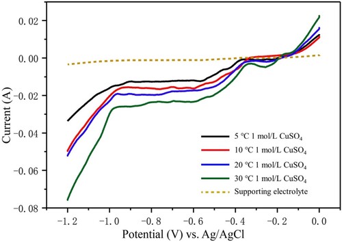
Prior to the printing, electrodeposition of Cu at different temperatures was investigated. For this purpose, linear sweep voltammetry (LSV) was employed to examine the electrochemical processes of metal reduction. A solution containing 0.4 M CuSO4 and 0.6 M H2SO4 was used as the electrodeposition electrolyte, and an H2SO4 solution with a pH of ∼4 was used as the supporting electrolyte. LSV curves for different temperatures are presented in . The essentially featureless LSV curve (dotted line in ), representing the supporting electrolyte without metal ions, indicates the absence of electrochemical reactions occurring in the supporting electrolyte within the displayed voltage window. The electrodeposition LSV curves of CuSO4 are indicated by solid lines, where different colours represent LSV curves measured at different temperatures. The onset potentials of Cu reduction at temperatures of 30, 20, 10, and 5 °C were –0.35, –0.37, –0.37, and –0.4 V, respectively. However, visual changes in the electrode appearance occurred only around –0.4, –0.43, –0.47, and –0.5 V, respectively. At these potentials, the electrodeposition rate increased and were acceptable because low electrodeposition rate made the printing process take more time. So, the potential selected for printing should be equal to or more than −0.5 V. Additionally, a lower temperature corresponded to a smaller cathodic current, but the difference was insignificant. A possible explanation is that the rate of ion diffusion during electrodeposition decreased with a reduction in the temperature. This confirms that the cold liquid environment slowed the diffusion of metal ions. When the potential was below –0.9, –0.93, –0.95, and –0.98 V at temperatures of 30, 20, 10, and 5 °C, respectively, the cathodic current increased rapidly with a reduction in the potential for all the LSV curves, which was attributed to the hydrogen evolution reaction on the working electrode. The happen of the hydrogen evolution could cause the density decrease of the deposits. So, the potential selected for printing should be less than or equal to −0.9 V. According to these results, a potential window of –0.5 to –0.9 V was suitable for the printing experiment.
Figure 3. Voltammetry of the electrodeposition electrolyte at different temperatures, as well as the supporting electrolyte.
3.4 Effects of temperature on printing
Voltammetry provides information on the electrodeposition process at different temperatures and was useful for selecting a suitable potential window for the printing experiment. As mentioned previously, the temperature affects the diffusion process of metal ions in the supporting electrolyte; thus, it is an important process parameter of microprinting. In this study, the effects of the temperature on the printing were examined. Before the printing, the potential and the pressure, which determine the electrodeposition rate of the metal plating process and the mass transport rate of metal ions ejected from the nanopipette aperture, should be selected. According to the aforementioned results, a potential of –0.6 V and a pressure of 5 mbar were applied. The initial gap between the nanopipette aperture (with an opening size of 500 nm) and the working electrode was set as 40 μm, and the gap was kept constant during the microprinting. presents scanning electron microscopy (SEM) images of the printed deposits obtained at temperatures of 30, 20, 10, and 5 °C. As shown, the printed deposits exhibited conical shapes, and their bottom diameters were 58.1, 41.4, 29.7, and 23.5 μm at 30, 20, 10, and 5 °C, respectively. This suggests that the deposition area can be reduced by decreasing the temperature of the electrolytes during the microprinting and confirms that a cold liquid environment can reduce the diffusion range of metal ions in the supporting electrolyte.
Figure 4. SEM images of the printed deposits obtained in the electrolytes at temperatures of (a) 30 °C, (b) 20 °C, (c) 10 °C, and (d) 5 °C.
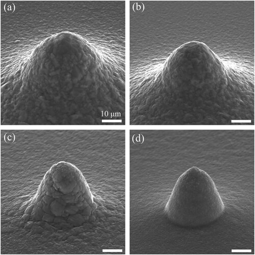
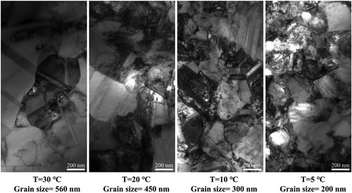
Additionally, the surface quality of the printed deposits was affected by the temperature. As shown, the roughness of the deposits decreased significantly with a reduction in the temperature. When the temperature decreased to 5 °C, the roughness of the deposits decreased to the nanoscale, implying that printed deposits with good surface quality were achieved at low temperatures, as shown in (d). One possible reason for this is that the amount of stray electrodeposition on the printed surface decreased. The stray electrodeposition resulted from the large-scale diffusion of the metal ions in the supporting electrolyte during the microprinting and degraded the surface quality of the deposits. The cold liquid environment reduced the diffusion range of metal ions, reducing the amount of stray electrodeposition. Another possible reason is that the grain size of the deposits decreased with the reduction in the temperature, as shown in . The grain sizes of the deposits obtained at 30, 20, 10, and 5 °C were approximately 560, 450, 300, and 200 nm, respectively. Previous studies indicated that reducing the grain size could improve the surface roughness of the deposits [Citation29,Citation30]. Additionally, the minimum printing size is significantly affected by the grain size of the electrodeposits. Theoretically, a smaller grain size corresponds to a smaller printing size. Thus, reducing the temperature may improve the printing resolution. Moreover, the TEM image implied that the printing deposits obtained at the low temperature are dense and polycrystalline.
Figure 5. Transmission electron microscopy (TEM) images of the printed deposits obtained in the electrolytes at temperatures of 30, 20, 10, and 5 °C.
These results confirm that the cold liquid environment increased the electrodeposition localisation and improved the printing quality. In this study, a low temperature of 5 °C was selected for printing via the CCLE technique, at which not only a small electrodeposition area but also high-quality and dense deposits could be achieved.
3.5 Optimisation of CCLE printing
An analysis of the effects of the temperature on the microprinting indicated that the CCLE technique can compress the electrodeposition area and improve the printing quality of the printed deposits, but further study of other parameters is needed, such as the potential and pressure, as mentioned previously.
In addition to the temperature, the potential and pressure are important process parameters for the microprinting, as they determine the rate of the metal electrodeposition and the transport rate of electrodeposition electrolyte ejected from the nanopipette aperture. These two parameters must be optimised to control the shape, size, and morphology of the printed deposits. It seems that the choice of the potential is obvious: a higher potential results in faster printing. However, very fast growth is detrimental, as it can result in complete or partial nozzle clogging [Citation22]. Regarding the pressure, it must not be too low or high: a pressure that is too low does not allow the electrodeposition electrolyte to flow out of the nanopipette, and a pressure that is too high makes the nanopipette inject too much electrodeposition electrolyte, causing uncontrolled distribution of the electrodeposition electrolyte in the supporting electrolyte. Thus, a potential window within –0.6 to –0.8 V and a pressure window within 1–5 mbar was selected for parameter optimisation. The optimisation was conducted by printing pillar arrays (). Micropillar printing is relatively simple but allowed us to obtain insights into the printing process. Each array consisted of nine pillars: three rows with different electrodeposition potentials and three columns with different pressures. Each pillar was fabricated until the total height reached 10 μm through a voxel-by-voxel process, with a stack of 50 voxels each 200 nm tall. A small voxel height caused a large amount of time to be spent on translation between voxels in the printing process. Conversely, when the voxel height was far larger, the increased distance between the nanopipette and printings resulted in a long time for ion collection, causing a large diffusion range of metal ions and increasing the deposition area [Citation24]. The printed Cu pillars with the set height of 10 μm were shown in (a), which had an actual total height ranged from 9.5∼10.3μm. The difference between the set height and the actual height might be due to the motion error or measurement error. Their average diameters ranged from 0.59 ± 0.09 μm (–0.7 V and 1 mbar) to 2.21 ± 0.21 μm (–0.5 V and 5 mbar). As shown, the CCLE technique could print pillars with a minimum diameter of 590 nm using the nanopipette with a 500-nm aperture, whereas FluidFM could print pillars with a minimum diameter of 800 nm a using nanotip with a 300-nm aperture, as previously reported, implying that the CCLE technique can print finer pillars with a larger aperture. This confirms that the cold liquid environment reduced the deposition area, helping the CCLE technique realise sub-microscale 3D printing.
Figure 6. Effects of the potential and pressure on printing via the CCLE technique: (a) SEM images of the printed pillars; (b) ratio of the top diameter to the bottom diameter (dt/db) for the pillars obtained with different parameters; (c) magnified SEM micrographs of pillars printed at –0.7 V and 1, 3, and 5 mbar.
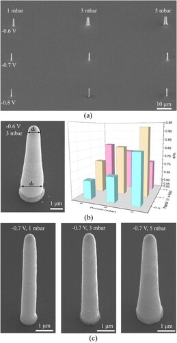
As shown in (b), the top diameter of the printed pillar was normally smaller than the bottom diameter. This is because the collection efficiency of metal ions cannot be 100%. Numerous metal ions diffused and induced undesirable deposition on the printed voxels, resulting in uniform deposits. The ratio of the top diameter to the bottom diameter (dt/db) of pillars is used to characterise the uniformity of deposits. The printed pillar is absolutely uniform if dt/db = 1. In the 3D histogram of (b), the height of each column represents the dt/db value. A higher column indicates a dt/db value closer to 1. When the potential was –0.6 V, dt/db decreased with an increase in the pressure; it was 0.81, 0.69, and 0.65 at 1, 3, and 5 mbar, respectively. The dt/db value exhibited a similar trend with respect to the pressure at a potential of –0.7 V; it was 0.92, 0.82, and 0.73 at 1, 3, and 5 mbar, respectively. This is because more metal ions were injected into the supporting electrolyte at the higher pressure, resulting in more metal ions being electrodeposited at the bottom of the pillar. However, dt/db exhibited the opposite trend with respect to the pressure at a potential of –0.8 V; it was 0.72, 0.78, and 0.81 at 1, 3, and 5 mbar, respectively. This may be because the reduction rate of metal ions was high at –0.8 V, but the metal ions were insufficiently supplied at low pressures, resulting in a nonuniform distribution of metal ions as well as nonuniform deposits. According to the dt/db results, the pillars printed at –0.7 V were relatively uniform – particularly at the pressure of 1 mbar – as shown in (c). Additionally, these pillars had sub-microscale diameters, and their surfaces were smooth. Thus, the CCLE technique can print uniform structures with high-quality surfaces at the sub-microscale through optimisation of the pressure and potential.
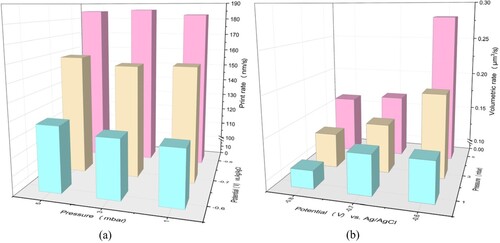
In addition to the shape, size, and morphology of the printed deposits, the print rate is an important concern for metal printing. In this study, the print rate was calculated by dividing the height of each pillar by its printing time. As shown in (a), the print rate was affected by the potential but was hardly affected by the pressure. The print rate was approximately 120, 160, and 190 nm/s at potentials of –0.6, –0.7, and –0.8 V, respectively, indicating that a lower potential resulted in a slower printing process. The pressure for electrolyte delivery also plays an important role in metal printing. Because the pressure significantly affected the pillar diameter, as shown in (a), the volumetric rate was used to represent this growth feature. As shown, when the potential was –0.6 V, the volumetric rate was initially 0.137 μm3 s−1 at 1 mbar, increased to 0.193 μm3 s−1 at 3 mbar, and increased to 0.281 μm3 s−1 at 5 mbar. Printing at –0.7 and –0.8 V exhibited similar trends. The volumetric rates were 0.137 μm3 s−1, 0.15 μm3 s−1 and 0.169 μm3 s−1 at 1, 3, and 5 mbar when the potential was –0.7 V. And They were 0.11 μm3 s-1, 0.132 μm3 s-1 and 0.163 μm3 s-1 when the potential was –0.8 V. It implied that the volumetric rate increased with the pressure. Besides that, it also implied that the volumetric rate decreased from −0.6 V to −0.8 V at the same pressure. The volumetric rate is determined by the reaction amount of the metal ions per unit time. And the reaction amount of the metal ions per unit time is determined by the reaction rate and the reaction area (Here the reaction area is the contact area between the electrodeposition electrolyte and the printing pillar). The increase of the volumetric rate with the pressure is because the diffusion range of the electrodeposition electrolyte increase with the pressure, which increases the reaction area. A possible explanation for the decrease of volumetric rate with the potential is that the reaction area decreases with the potential because the diameter of pillar decreases with the potential when the pressure keeps constant. Compared with the previous reports, this study has much lower print rate and volumetric rate[Citation19,Citation22]. For the print rate, this is attributed to the low reaction current () caused by the low mass transfer rate in the cold liquid environment. For the volumetric rate, it is attributed to the fact that the cold liquid environment reduced the diffusion range of the electrodeposition electrolyte in the supporting electrolyte. The low volumetric rate confirmed that the cold liquid environment reduced the deposition area and enhanced the electrodeposition localisation.
Figure 7. (a) Print rate and (b) volumetric rate of the CCLE technique.
3.6 Edx spectrum and inner microstructure of printed pillar
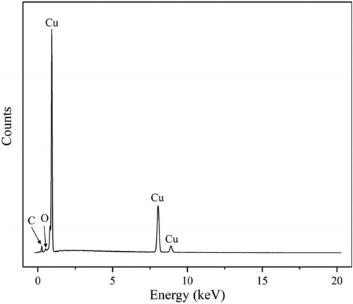
The temperature is an important process parameter of electrodeposition. Normally, electrodeposition is conducted in the electrolytes with the temperature above 30 °C, but in this study, the Cu pillars were electrodeposited in the electrolytes at a temperature of 5 °C. There have been few studies on the metal purity and the microstructure of metals electrodeposited below 5 °C. The metal purity and microstructure are important performances in some applications, that influence the electrical or optical properties. Thus, the metal purity and inner microstructure of the printed pillar was investigated. Here the energy-dispersive X-ray spectroscopy (EDX) was used to assess the metal purity of the printing deposits. showed the EDX spectrum of the printing pillar. As seen, Cu, O and C elements were found in this spectrum, and the peak intensity of Cu was far greater than that of O and C. The wt% of Cu was more than 95%, meaning that the printing deposits was pure copper. The small content of O and C might be attributed to the air contamination (such as organic matter) during post-printing handling. Because neither the electrodeposition electrolyte nor the supporting electrolyte contained C element during the printing.
Figure 8. EDX spectrum of the printing deposits
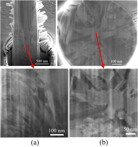
The longitudinal and transverse sections of the pillar printed at –0.7 V and 1 mbar were exposed using a focused ion beam (FIB), as shown in . The ‘lamellar’ structure outside the pillar was a protective layer (95 wt% Pt and 5 wt% C) that was sputtered on the surface before FIB milling to improve the flatness of the sections. Both the longitudinal and transverse sections revealed that the inner microstructure of the pillar was dense, without voids, micropores, or other defects between voxels. It implied that the stratifications did not happen during the printing. Additionally, the pillar had a polycrystalline microstructure, and the grain size was approximately 150–200 nm. Further observation of the transverse section indicated that the grains were elongated and extended from the pillar centre outward, which is conducive to achieving a high surface quality. Overall, the internal structure of the printed pillar indicated that the CCLE technique can print structures with dense and crystalline inner microstructures without any stratifications, which is in accordance with the results of the TEM determination in .
Figure 9. FIB-SEM (a) longitudinal section and (b) transverse section images of the printed pillars at −0.7 V and 1 mbar.
3.7 Printing of 3D structure and pillar with high aspect ratio
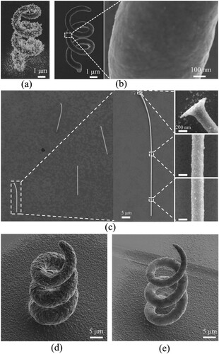
The microprinting process of the CCLE technique was studied and optimised, and the results indicated that the uniform pillars with high-quality surfaces and dense and crystalline microstructures were achieved at the sub-microscale. However, the pillar is the simplest 3D structure, and the printed pillars had small heights. The realisation of uniform complex 3D structures or pillars with high aspect ratios and high-quality surfaces at the sub-microscale is often challenging. Therefore, in this study, a helix and pillars with a high aspect ratio of 172:1 were prepared at the sub-microscale to analyse the capability of the CCLE technique (). As a comparison, a helix with a total height of ∼12 μm and line diameter of 1.8 μm was printed using a nanopipette with a 500-nm aperture at the temperature of 30 °C, that was showed in in (a). The printing parameters, i.e. the potential, pressure, and voxel height, were –0.7 V, 1 mbar, and 200 nm, respectively. It took about 5 mins to print this helix. As seen, this helix had lots of dendrites on the surface. One reason was that a severe stray deposition happened on its surface. The other reason might be that the component of the electrodeposition electrolyte in the printing area significantly changed due to the high diffuse rate on metal ions, resulting in the abnormal electrodeposition. (b) shows a helix with a total height of ∼12 μm and line diameter of 850 nm printed at the temperature of 5 °C by using the same parameters in 9 mins. As seen, the diameter of the helix remained unchanged along the rising direction except at the end of the helix. The reduction in the diameter in this part is attributed to the clogging of the nanopipette by the deposits. A magnified image indicated that the printed helix had a smooth surface. Comparing the diameter and the surface quality in (a,b), it can be drawn an intuitive conclusion that the deposition area significantly reduced at the low temperature. As shown in (c), pillars with a total height of ∼50 μm and diameter of 290 nm were printed using a nanopipette with a 200-nm aperture. The potential, pressure, temperature, and voxel height of the printing were –0.7 V, 3 mbar, 5 °C, and 200 nm, respectively. The printed pillars fell easy during the post-printing handling. This is because their aspect ratio (172:1) was too high, and the adhesion between the pillars and the substrate was not strong enough to maintain the stability of the pillars. A magnified image indicated that the diameter of the pillar remained unchanged along the printing direction and that the surfaces were relatively smooth. For the printed structures at the temperature of 5 °C, almost all the deposition occurred directly on the structures, and there was little deposition on the substrate around them. Thus, we consider that the low temperature restricted the large-scale diffusion of metal ions inside the supporting electrolytes, reducing the amount of undesirable electrodeposition on the formed structures and the substrate around the structures. This makes it possible to prepare high-quality, high-strength and good-conductivity complex 3D structures at the sub-microscale.
Figure 10. SEM images of the printed (a) helix at 30 °C with pressure of 1 mbar, (b) helix at 5 °C with pressure of 1mbar, (c) pillars with a high aspect ratio at 5 °C, (d) helix at 30 °C with pressure of 10 mbar and (e)helix at 5 °C with pressure of 10 mbar.
In further researches to printing larger scale structures (mainly increase the printing line width), the pressure of 10 mbar was applied to deliver more metal ions into the supporting electrolyte. Here helixes with total heights of ∼60 μm were printed using a nanopipette with a 500-nm aperture at the temperature of 30 and 5 °C respectively. The printing needed 21 and 39 mins to accomplish. As seen, the line diameter of the helix printed at 30 °C is about 12 μm, and its surface is quite rough. Moreover, the helix line at different layers almost connects to be a surface because the line diameter is too large. As expected, the line diameter of the helix printed at 5 °C decreases to 5 μm, and the surface quality increase apparently. As above mentioned, this is because the low temperature restricts the diffusion of metal ions, decreases the electrodeposition area and reduces the electrodeposition quantity on the surface of the printed structure. However, different with the helix printed with the pressure of 1mbar at 5 °C showed in (b), it found that metal electrodeposition happens on the substrate around the structures with the pressure of 10 mbar. Comparing the structures in (b,d,e), it thinks the effect of low temperature on improving printing quality is still effective at a much higher pressure. But too much metal ions delivered in unit time decreases this effect, resulting in the undesired electrodeposition on the substrate around the printed structure.
Therefore, CCLE already shows its high potential to print high-quality structures at the sub-microscale. While it needs to further optimise the printing process and parameters to prepare structures without undesired electrodeposition on the substrate at larger scales.
3.8 Mechanical property of printed pillars
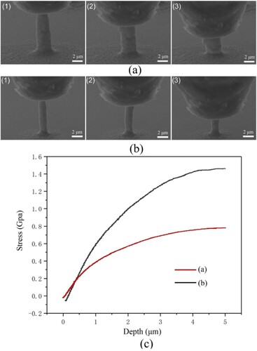
The mechanical properties of the printed at 30 °C and 5 °C are measured by micro-compression experiments, and the deformation process can be observed using in-situ SEM. During the measurement, a flat diamond indenter, with a diameter of 5 μm, was used to compress the printed pillars at a constant speed of 40 nm/s. The printed pillars have geometric deviations from an ideal cylindrical. The top and bottom of the pillars are both rounded, and the bottom diameter is larger than the top diameter. So, the stress was calculated using the bottom diameter of the pillars. The deformation process of the pillars printed (printing potential and pressure are −0.7 V and 5 mbar) at 30 °C and 5 °C are shown in (a,b) respectively, and the stress-depth curves are presented in (c). As seen, both the stress-depth curves have elastic and plastic deformation stages. It implies that the pillars printed at 30 °C and 5 °C both have good mechanical stability. As further seen, the maximum stress of the pillar printed at 30 °C is about 0.75 GPa at the depth of 5 μm. That is in acceptable agreement with values for printed pillars in previous reported [Citation19], which ranged from 0. 7 to 0.9 GPa. While the maximum stress of the pillar printed at 5 °C is about 1.45 GPa at the depth of 5 μm. That means the pillar printed at 5 °C can bear a much larger load. This is because that the printing deposits at 5 °C has a much smaller grain size as shown in . So, it can be concluded that CCLE can prepared printed structures with high strength.
Figure 11. In-situ SEM micro-compression experiment on Cu pillars printed at different temperatures: (a) pillar printed at 30 °C, (b) pillar printed at 5 °C, (c) the stress and the depth of the diamond tip in the experiment.
lists the published descriptions on two main EC printing techniques (MCED and FluidFM) and corresponding descriptions on CCLE. As seen, although CCLE shows the advantages in surface quality and strength, but it needs further improvement in print rate and ability of fabricating complex 3D structure.
Table 2. Published descriptions on MCED and FluidFM and corresponding descriptions on CCLE.
4. Conclusions
We propose a novel CCLE technique for sub-microscale 3D metal printing based on locally confined electrodeposition of precursors in liquid. During the printing, the electrolytes are cooled to 5 °C, which constrains the large-field diffusion of the electrodeposition electrolyte in the supporting electrolyte and allows a far smaller electrodeposition area to maintain the component stability of the electrodeposition electrolyte in the printing area. Pillar arrays of Cu were printed with different pressures and potentials, resulting in the fabrication of uniform sub-microscale pillars with high-quality surfaces and dense crystalline microstructures after parameter optimisation. The printing of a helix and pillars with a high aspect ratio of 172:1 revealed that the CCLE technique can be used to prepare challenging sub-microscale (minimum size is low to 290 nm) 3D metal microstructures that are uniform and of high quality. Besides that, CCLE can prepared printed structures with high strength.
This study demonstrated the potential of local microelectrochemical 3D printing for producing sub-microscale metal microstructures via the CCLE technique, making it possible to prepare high-quality, high-strength and good-conductivity complex 3D structures in the industry. Although only electrochemical printing of Cu was examined in this study, advances in the CCLE technique can allow the microprinting of other electroplatable metals. Additionally, in future research, we will investigate the possibility of nanoscale printing via the CCLE technique by further reducing the temperature and reducing the aperture size of the nanopipette. Also, the printing process and parameters of the CCLE technique will be further optimised to prepare structures at larger scales.
Disclosure statement
No potential conflict of interest was reported by the author(s).
Data availability statement
Data available on request from the authors.
Additional information
Funding
References
- Lewandowski JJ, Seifi M. Metal additive manufacturing: A review of mechanical properties. Annu Rev Mater Res. 2016;46:151–186. doi:10.1146/annurev-matsci-070115-032024
- Zinovieva O, Zinoviev A, Ploshikhin V. Three-dimensional modeling of the microstructure evolution during metal additive manufacturing. Comput Mater Sci. 2018;141:207–220. doi:10.1016/j.commatsci.2017.09.018
- Song XF, Liaw PK, Wei ZY, et al. Evolution of the microstructures, magnetic and mechanical behaviors of Co47.5Fe28.5Ni19Si3.4Al1.6 high-entropy alloy fabricated by laser powder bed fusion. Addit Manuf. 2023;71:103593
- Maurel A, Pavone A, Stano G, et al. Manufacturing-oriented review on 3D printed lithium-ion batteries fabricated using material extrusion. Virtual Phys Prototy. 2023;18:e2264281.
- Gradl PR, Protz CS. Technology advancements for channel wall nozzle manufacturing in liquid rocket engines. Acta Astronaut. 2020: 174.
- Tan C, Weng F, Sui S, et al. Progress and perspectives in laser additive manufacturing of key aeroengine materials. Int J Mach Tool Manu. 2021;170:103804), doi:10.1016/j.ijmachtools.2021.103804
- Fischer J, Wegener M. Three-dimensional optical laser lithography beyond the diffraction limit. Laser Photonics Rev. 2013;7:22–44. doi:10.1002/lpor.201100046
- Sochol RD, Sweet E, Glick CC, et al. 3D printed microfluidics and microelectronics (2018). Microelectron Eng. 2017;189:52–68.
- Hirt L, Reiser A, Spolenak R, et al. Additive Manufacturing of Metal Structures at the Micrometer Scale. Adv Mater. 2017;29:e1604211.
- Wang H, Chen C, Yang F, et al. Direct ink writing of metal parts with curing by UV light irradiation. Mater Today Commun. 2021;26:102037.
- Chang H, Guo R, Sun Z, et al. Flexible conductive materials: direct writing and repairable paper flexible electronics using nickel–liquid metal Ink. Adv Mater Interfaces. 2018;5:1870097), doi:10.1002/admi.201870097
- Merrow H, Beroz JD, Zhang K, et al. Digital metal printing by electrohydrodynamic ejection and in-flight melting of microparticles. Addit Manuf. 2021;37:101703.
- Park JU, Hardy M, Kang SJ, et al. High-resolution electrohydrodynamic jet printing. J A Rogers, Nat Mater. 2007;6:782–789. doi:10.1038/nmat1974
- Utke I, Michler J, Winkler R, et al. Mechanical properties of 3D nanostructures obtained by focused electron/Ion beam-induced deposition: A review. Micromachines (Basel). 2020;11(4):397), doi:10.3390/mi11040397
- Diercks DR, Gorman BP, Mulders JL. Electron Beam-Induced deposition for atom probe tomography specimen capping layers. Microsc Microanal. 2017;23:321.
- Utke I, Hoffmann P, Melngailis J. Gas-assisted focused electron beam and ion beam processing and fabrication. J Vac Sci Technol B Nanotechnol Microelectron Mater, Process, Meas, Phenom. 2008;26:1197–1276.
- Lin JC, Yang JH, Chang TK, et al. On the structure of micrometer copper features fabricated by intermittent micro-anode guided electroplating. Electrochim Acta. 2009;54(24):5703–5708. doi:10.1016/j.electacta.2009.05.015
- Lin YP, Zhang Y, Yu MF. Parallel process 3D metal microprinting. Adv Mater Technol. 2019;4:1800393), doi:10.1002/admt.201800393
- Hirt L, Ihle S, Pan ZJ, et al. 3D microprinting: template-free 3D microprinting of metals using a force-controlled nanopipette for layer-by-layer electrodeposition. Adv Mater. 2016;28:2277), doi:10.1002/adma.201670077
- Momotenko D, Page A, Adobes-Vidal M, et al. Write–read 3D patterning with a dual-channel nanopipette. ACS Nano. 2016;10:8871–8878. doi:10.1021/acsnano.6b04761
- Reiser A, Lindén M, Marchand A, et al. Multi-metal electrohydrodynamic redox 3D printing at the submicron scale. Nat Commun. 2019;10(1):1853), doi:10.1038/s41467-019-09827-1
- Ercolano G, Zambelli T, Nisselroy CV, et al. Multiscale additive manufacturing of metal microstructures. Adv Eng Mater. 2020;22:1900961.
- Seol SK, Kim D, Lee S, et al. Electrodeposition-based 3D printing of metallic microarchitectures with controlled internal structures. Small. 2015;11:3896–3902.
- Nisselroy C, Shen C, Zambelli T, et al. Addit Manuf. 2022;53:102718.
- Shen C, Zhu Z, Zhu D, et al. Electrochemical 3D printing of Ni–Mn and Ni–Co alloy with FluidFM. Nanotechnology. 2022;33(26):265301), doi:10.1088/1361-6528/ac5a80
- Holz M, Heil SR, Sacco A. Temperature-dependent self-diffusion coefficients of water and six selected molecular liquids for calibration in accurate 1H NMR PFG measurements. Phys Chem Chem Phys. 2000;2:4740–4742. doi:10.1039/b005319h
- Jiao Y, Zhuang J, Zhang T, et al. Research on the adaptive sensitivity scanning method for ion conductance microscopy with high efficiency and reliability. Anal Chem 2021; 93:12296–12304.
- Dorwling-Carter L, Aramesh M, Han H, et al. Combined ion conductance and atomic force microscope for fast simultaneous topographical and surface charge imaging. Anal Chem. 2018;90:11453–11460.
- Groche P, SchFer R, Justinger H, et al. On the correlation between crystallographic grain size and surface evolution in metal forming processes. Intern J Mech Sci. 2010;52(3):523–530. doi:10.1016/j.ijmecsci.2009.11.017
- Wei J, Shen L, Qiu M, et al. Microhardness, wear, and corrosion resistance of Ni-SiC composite coating with Magnetic-Field-assisted jet electrodeposition. Mater Res Express. 2018;5:096407–096407.
- Wang YT, Xiong X, Ju BF, et al. Voxelated meniscus-confined electrodeposition of 3D metallic microstructures. Int J Mach Tool Manu. 2022;174:103850), doi:10.1016/j.ijmachtools.2022.103850
- Hengsteler J, Mandal B, Nisselroy C, et al. Bringing electrochemical three-dimensional printing to the nanoscale. Nano Lett. 2021;21(21):9093–9101. doi:10.1021/acs.nanolett.1c02847
- Hengsteler J, Kanes KA, Khasanova L, et al. Beginner's guide to micro- and nanoscale electrochemical additive manufacturing. Annu Rev Anal Chem. 2023;16(1):71–91. doi:10.1146/annurev-anchem-091522-122334