
 ?Mathematical formulae have been encoded as MathML and are displayed in this HTML version using MathJax in order to improve their display. Uncheck the box to turn MathJax off. This feature requires Javascript. Click on a formula to zoom.
ABSTRACT
A metamaterial can be used for fabricating an electromagnetic absorber by tailoring its effective permittivity and permeability. In general, a metamaterial absorber works at a specific resonant frequency, and its absorption frequency does not change after the structure is fabricated. A three-dimensionally (3D)-printed shape memory polymer (SMP) is a potential candidate for overcoming this limitation and realising reconfigurability with its fabrication versatility. In this work, we propose a frequency – and bandwidth-controllable electromagnetic absorber using 3D-printed shape memory meta-wires (SMMWs). Unlike the conventional usage of SMPs with two states, thermally deformable SMMWs have three different modes that are realised by controlling the states of each column. Multi-material additive manufacturing is used to print the SMMW, with an SMP substrate and a high-temperature filament being the materials that are printed. The high absorptivity and frequency – and bandwidth-tuning capability are numerically and experimentally demonstrated for three different modes.
1. Introduction
Metamaterial absorbers (MMAs) have several advantages such as high absorptivity and low thickness compared to other types of electromagnetic wave absorbers. MMAs operate with LC resonance; however, the absorption frequency bandwidths are too narrow to cover a wide range. Therefore, MMAs with different designs have been studied in various frequency bands. For example, MMAs using multi-resonators [Citation1–11], resistive conductive patterns [Citation12–14] and lumped resistors [Citation15–17] have been introduced. Nevertheless, MMAs work only at specific resonant frequencies and do not undergo frequency changes after fabrication. This constraint significantly limits their applications. Consequently, the necessity for reconfigurable MMAs has emerged and their development has continued.
There have been many different types of reconfiguration methods, including electrical, mechanical, fluidical and thermal methods. MMAs using the electrical reconfiguration method have PIN diodes or varactor diodes on their patterns or grounds [Citation18–25]. By applying different input-bias voltages, the absorption frequency can be controlled. Moreover, MMAs using the mechanical reconfiguration method require an external mechanical force to change the structures [Citation26–29]. For example, actuators that can control the height of an air layer of an MMA have been proposed [Citation30]. Further, fluidically reconfigurable MMAs can change the operating frequency bands by injecting liquid metal into the substrates [Citation31–33]. Unlike these MMAs, thermally reconfigurable MMAs use smart materials such as shape memory alloy [Citation34, Citation35] and shape memory polymer (SMP) to change the operating frequency. Because these smart materials can memorise the original state, they can be recovered by any external stimulus.
SMP is a material that has the ability to restore from a deformed state to the original state under external stimuli [Citation36]. Generally, an SMP has two states, namely, glassy and rubber states, which are determined by external temperature [Citation37]. When heat above the transition temperature () is applied to the SMP, it becomes flexible like a rubber. The SMP in the rubber state is capable of being deformed with force, and its geometry remains fixed in the glassy state after cooling down. Remarkably, the deformed geometry can be recovered to the original geometry when temperature is higher than
. This versatile material has recently been developed as a filament for three-dimensional (3D) printing purposes [Citation38] that memorises the initially printed geometry.
3D printing is a technology that is employed to fabricates 3D structures using guided digital modelling data. There are several categories of 3D printing technologies, including powder bed fusion [Citation39–41], vat photopolymerization [Citation42, Citation43], and material extrusion. One of the representative methods of material extrusion is fused deposition modelling (FDM), which utilises a heated nozzle to melt filaments such as polylactic acid (PLA) and deposits these semiliquid materials layer by layer [Citation44, Citation45]. As mentioned above, SMP filament for 3D printing has been developed, which enables the utilisation of its remarkable advantages in manufacturing processes. In addition, 3D-printing-based manufacturing is cost-effective compared to other manufacturing processes, which enhances its competitiveness [Citation46].
In this paper, we present an electromagnetic absorber (EMA) fabricated using 3D-printed shape memory meta-wires (SMMWs) to achieve functionality with controllable resonant frequency and bandwidth. Remarkably, the proposed EMA has three modes that are realised by thermally deformable SMMWs which can be controlled by columns unlike other works. SMMWs are printed by multi-material additive manufacturing technology to use both SMP and high-temperature filaments for stable deformation. We utilised a dual-nozzle 3D printer to print the SMMWs, allowing the simultaneous use of both filaments in a single process. Additionally, silver paste was employed to realise conductivity. The high absorptivity and frequency-tuning capability were predicted by numerical electromagnetic analysis and experimentally demonstrated for all three modes. We also tested the restoration repetition of the fabricated sample for 70 cycles, and the repeatability has been checked with the same simulated absorptivity for each cycle.
2. Numerical analysis
2.1. Unit cell design
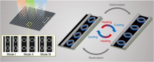
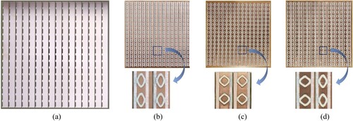
We utilised the ANSYS high-frequency structure simulator (HFSS) for design and electromagnetic simulation, and multi-material 3D printing for fabrication. shows the proposed EMA fabricated using 3D-printed SMMWs. The EMA, inspired by kirigami structures, was designed for the columns of SMMWs to be individually stretched and restored by external stimuli. The absorption frequency varies when the columns of the EMA are deformed, and it returns to its original frequency when the columns are restored to its initial state. For example, the EMA operates in Mode I when all its columns are in their original states. In this mode, it exhibits a specific absorption frequency. However, when all the columns are deformed, it transitions to Mode II, resulting in a variation in the absorption frequency. Remarkably, when the columns are restored, the EMA reverts to Mode I. In addition to the original (Mode I) and deformed (Mode II) states, each column of the SMMWs can be adjusted to create an alternating column sequence. This allows the EMA to operate in another mode (Mode III) with an expanded bandwidth.
Figure 1. Conceptual illustration of the proposed electromagnetic absorber using 3D-printed SMMWs.
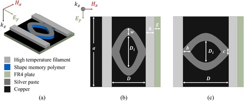
shows the composition and geometries of the unit cell. As shown in (a), the unit cell comprises a 3D-printed SMMW and an FR4 plate. The 3D-printed SMMW is 1.1 mm thick and composed of a high-temperature (HT) filament which is a heat-resistant material and SMP filament. We used two different filaments to form a proper geometry because the consistent deformation process cannot be reliably conducted using SMP alone (further discussed in Section 3). The dielectric constant of HT filament is 1.94 with a loss tangent of 0.07, whereas SMP filament has 3 and 0.03, respectively. Additionally, silver paste is applied on the SMP to achieve conductivity. A 1-mm-thick FR4 plate (dielectric constant = 3.9 and loss tangent = 0.02) [Citation47, Citation16] is under the SMMW and covered with copper on top. Therefore, silver and copper boundaries were respectively assigned to the top of SMP and FR4 plate with a finite conductivity in simulation. (b) shows the original state of the unit cell and its parameters with the following dimensions: a = 18 mm, b = 1.95 mm, c = 1.5 mm, g = 1.5 mm, h = 2.3 mm, w = 2.025 mm, = 8.25 mm, and D = 8.7 mm. Further, (c) shows the deformed state and its parameters with the following dimensions:
= 5.55 mm and
= 11.7 mm. The parameter
represents the inner gaps of the conductive patterns, while D denotes the distances between the frame parts. Finally, the complete design of the EMA comprises a total of 16 × 16 unit cells, and it is 288 mm × 288 mm in size.
Figure 2. Unit cell design and geometries: (a) material composition, (b) original state, and (c) deformed state.
The absorptivity, , can be calculated by using the following equation:[Citation4]
(1)
(1) where
and
are reflection and transmission coefficients, respectively. In general,
is determined by the impedance of the EMA and its equation is as follows:
(2)
(2) where
and
are the impedances of the EMA and free space (377 Ω), respectively. Because the bottom surface of the proposed EMA is not fully covered by a conductor,
has also been considered.
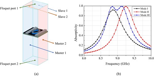
(a) presents boundary conditions and excitation ports. We assigned a master/slave boundary and excited the structure using floquet ports to simulate a periodic structure. The E-field at every point on the slave boundary surface is forced to match the E-field of every corresponding point on the master boundary surface, allowing a bounded structure to have an infinite periodicity. Also, floquet ports are used exclusively with periodic structures defined by master/slave boundaries and excite plane waves whose frequency, phase, and geometry of a structure decide the propagation direction. (b) shows the simulated absorptivity of the proposed EMA in three modes. The simulation result showed a peak absorptivity of 92.0% at 8.87 GHz and a bandwidth over 90% of 100 MHz from 8.81 to 8.91 GHz in Mode I. However, in Mode II, a peak absorptivity of 98.9% at 9.25 GHz and a bandwidth over 90% of 200 MHz from 9.15 to 9.35 GHz was observed. Moreover, Mode III exhibited two peaks of 98.8% and 99.3% at 8.84 and 9.13 GHz, respectively, along with an enhanced bandwidth of 460 MHz from 8.76 to 9.22 GHz.
Figure 3. Simulation setup and results: (a) boundary conditions and excitation ports, and (b) simulated absorptivity of the proposed EMA in three modes.
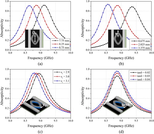
The parametric studies were also conducted to address the effect of the varying parameters such as and
, which are critical to the performance of the EMA. As shown in (a,b), we determined
and
as 8.25 and 2.025 mm, respectively. As we increase
from 7.75 mm to 8.75 mm, the resonant frequency decreases from 9.12 GHz to 8.63 GHz due to increased effective capacitance between the neighbouring cells in the horizontal direction. Additionally, the resonant frequency decreases from 9.36 GHz to 8.56 GHz as we increase
from 0.675 mm to 3.375 mm because of increased effective inductance generated from the conductive pattern. Moreover, we examined the impact of varying dielectric characteristics, including a dielectric constant and a tangential loss, through parametric simulations. (c) shows the effect of dielectric constant (
) of the SMP on the resonant frequency of the EMA. For instance, the resonant frequency decreases from 8.95 GHz to 8.79 GHz as
increases from 2.9 to 3.1. In addition, as we increases the tangential loss (tanδ) from 0.02 to 0.04, the absorptivity increases from 86.2% to 96.0% ((d)).
Figure 4. Parametric studies of unit cell’s geometrical parameters and dielectric characteristics: absorptivity for different (a) , (b)
, (c) dielectric constant (
), and (d) tangential loss (tanδ).
2.2. Equivalent RLC circuit
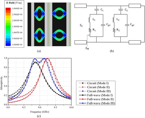
The proposed EMA can be expressed as an equivalent RLC circuit that is determined by the design of a unit cell and the interactions between neighbouring unit cells. shows the simulated electromagnetic field (E-field) distribution and the equivalent RLC circuit for four neighbouring unit cells. In (b), because the E-field is intensely distributed at the longitudinal edges of the pattern as shown in (a), we considered the capacitances between the unit cells in each column as and
. We also considered the capacitances (
,
), inductances (
,
), and resistances (
,
) generated by each SMMW. Capacitances
and
are realised by the inner gap of an SMMW, while inductances
and
, and resistances
and
are obtained by the conductive pattern on the top of an SMMW and its loss, respectively [Citation3, Citation11]. In Modes I and II,
equals
and all other corresponding pairs of capacitance, inductance and resistance are the same due to their identical geometries. The values for Mode I are calculated as follows:
=
= 0.0166 pF,
=
= 0.199 pF,
=
= 1.521 nH, and
=
= 2.163 Ω. However, in Mode II, the parameters exhibit different values, which are as follows:
=
= 0.0210 pF,
=
= 0.393 pF,
=
= 0.734 nH and
=
= 1.220 Ω. Because the columns of Modes I and II are alternating in Mode III, the values for Mode III are calculated as follows:
= 0.0166 pF,
= 0.199 pF,
= 1.521 nH,
= 2.163 Ω,
= 0.0210 pF,
= 0.393 pF,
= 0.734 nH and
= 1.220 Ω. Advanced Design System (ADS) was utilised for both value determination and circuit simulation. (c) presents absorptivity results from both circuit and full-wave simulation results across all different modes, demonstrating a good agreement between the circuit and the full-wave simulation.
Figure 5. Analysis of four neighbouring unit cells: (a) simulated electromagnetic field, (b) equivalent RLC circuit, and (c) RLC circuit simulation and full-wave simulation in different modes.
3. Fabrication
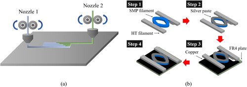
(a) illustrates the dual-nozzle FDM-type 3D printing (Sindoh 3DWOX 7X) that was used to fabricate SMMWs, whose stable shape memory characteristic was realised by using HT and SMP filaments (both are polylactic acid based filaments). Unlike single-nozzle 3D printers, a dual-nozzle 3D printer has an advantage in fabrication because it can print structures in which multiple materials are combined at once. Thus, we were able to fabricate a robust structure that could not be achieved with a single-nozzle printer made of only SMP [Citation48, Citation49]. of the SMP filament is 55 °C. Because we chose the deformation temperature as 75 °C to flexibly deform SMP filament (SMP Technologies Inc.), we also examined the heat deflection temperature of the filaments to select a proper filament to collaborate with the SMP. A widely used PLA filament (Sindoh Co.) has heat deflection temperature of 52 °C. It is lower than the deformation temperature, so the structure using PLA would be distorted. On the other hand, because HT filament (colorFabb Inc.) has a heat deflection temperature of 94 °C, it would not be distorted. Therefore, we set nozzles 1 and 2 to extrude the HT and SMP filaments, respectively. The nozzle temperatures were set to 250 and 210 °C for each filament. The bed temperature was initially set to 80 °C, which was sufficient for maintaining stable adhesion of the output for the SMP filament. However, the HT filament did not adhere properly, and the edges started to lift gradually owing to the temperature differences between the deposited layers. Because a high bed temperature guarantees improved adhesion, we set the bed temperature to 100 °C, considering the heat-sensitive characteristic of the SMP filament, to provide optimal adhesion without subjecting the filament to excessive temperatures. The deposition layer heights were identically set for both nozzles 1 and 2. We set the initial layer height to 0.3 mm and the subsequent layer height to 0.2 mm. By contrast, the printing speeds varied between the two filaments. We set the initial layer printing speed to 10 mm/s and the subsequent layer printing speed to 80 mm/s for the HT filament, while both the initial and subsequent layer printing speeds were set to 10 mm/s for the SMP filament. This condition was applied considering the heat sensitivity of the SMP filament that tends to stretch out when printed at high speeds. We measured the dielectric characteristics of the HT and SMP filaments using a T-resonator. The HT filament had a dielectric constant
= 1.94 and loss tangent = 0.07, and the SMP filament had a dielectric constant
= 3 and loss tangent = 0.03 for a material infill density of 1073.6 kg/m3, which is equivalent to 20%. As shown in (b), the SMMW comprises SMP filaments and a frame made of HT. The frame is extended to longitudinally neighbouring frames, enabling efficient control of the columns and facilitating mode transitions as a full structure. To achieve conductivity, elcoat P-100 silver paste, which dries within 12 hours at room temperature (25 °C), was applied on the SMP substrate of the SMMW. It was measured to have a bulk conductivity of
S/m. Although the silver paste is not stretchable, the silver pasted conductive pattern can keep its conductivity when stretched for D from 8.9 mm to 17.0 mm. Because
of the proposed unit cell deforms from 8.9 mm to 11.6 mm, we can use silver paste for deformable conductive patterns. In addition, an FR4 plate covered with copper on top was placed under the SMMW to act as a ground. The FR4 plate had a hole that facilitated the assembly of the SMMW.
Figure 6. Illustrations of the manufacturing process: (a) dual-nozzle FDM 3D printing and (b) step-by-step manufacturing process of the unit cell.
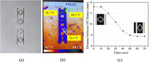
Before we fabricate the full structure of the proposed EMA, we first demonstrated the thermal profile of the SMMW. (a) presents a test sample of an SMMW. We placed the sample on a hot plate of 75 °C and captured a thermal image to check the thermal distribution as presented in (b). Because the temperature of SMP exceeds (55 °C), the geometry could be deformed by manually pulling the heat-durable HT frame. Furthermore, we addressed the structural deformation in terms of time as shown in (c). We initially deformed the sample to Mode II and then exposed it to a 75 °C hot plate. The distance between two HT frames decreased over time, and it took 60 s to recover the sample to its memorised geometry (Mode I).
Figure 7. Thermal profile of SMMW: (a) a sample of an SMMW, (b) a thermal image of the sample, and (c) structural deformation over time.
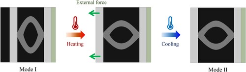
To reconfigurable the geometry back to Mode II, heating and cooling processes are required as presented in . Because the structure can be deformed when exposed to temperature higher than , we initially heat the structure and then apply an external force to move an HT frame. As HT frame aligns with the edge of a copper plate (D = 11.6 mm), the geometry can be fixed by cooling.
Figure 8. Reconfiguring process of the SMMW from Mode I to Mode II.
We fabricated the proposed EMA comprising 16 × 16 unit cells as a prototype sample. (a) shows the FR4 plate covered with copper on top, and its size is 300 mm × 300 mm. The plate has holes that are to be assembled with the columns of SMMWs. Because copper is physically separated by columns as shown in the figure, heat can be distributed to the individual columns. Therefore, each column can be deformed to make the EMA operate in different modes. We assembled all the columns of the SMMWs and heated each column to manipulate all three different modes. (b–d) show the EMA in Modes I, II and III, respectively. Mode I is the original state where the geometry of the SMMWs is memorised as = 12.6 mm and D = 8.9 mm. To transform Mode I to Mode II, we applied hot temperature (75 °C) on the SMMWs which are ready to be deformed. Next, the columns of the SMMWs are deformed by manually pulling the HT frames until
= 10.5 mm and D = 11.6 mm. Because Mode I is memorised, Mode II can be transformed back to Mode I by applying hot temperature (75 °C) on the SMMWs.
Figure 9. Fabricated EMA in different modes: (a) FR4 plate with holes. The EMA in (b) Mode I, (c) Mode II, and (d) Mode III.
4. Results
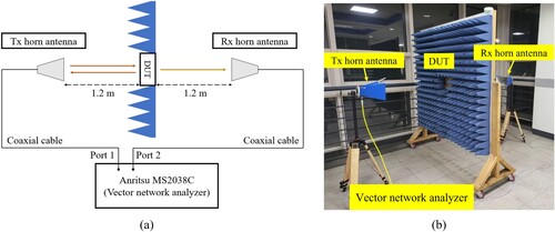
4.1. Measurement
shows the measurement setup for both reflection and transmission using two horn antennas. (a,b) respectively present an illustration and a photograph of the measurement setup. We utilised horn antennas (Dorado GH1-18N) with a bandwidth that covered the X-band. Two antennas faced each other, and a wedge tapered absorber (WTA) was placed in the middle of the antennas to minimise undesired reflection. We placed the sample at the center of the WTA because it had a square aperture that enabled transmission of electromagnetic waves. The distance between the antennas and the WTA was set as 1.2 m. Both Tx and Rx antennas were connected through coaxial cables to port 1 and port 2, respectively, of the Anritsu MS2038C vector network analyzer (VNA). The absorptivity was calculated by using EquationEquation (1)(1)
(1) . Reflection coefficient is measured using a Tx horn antenna connected to the VNA and the calibration is performed by normalising the reflection coefficient of the fabricated sample with that of the same sized copper plate. Thus, we can define total reflection (
) from the copper plate. Additionally, transmission coefficient is measured using both Tx and Rx horn antennas and the calibration is performed by normalising the transmission coefficient of the EMA with that of air. Thus, we can define total transmission (
) from air propagation without any obstacle. A time gating function is introduced to measure reflection only from the test prototype.
Figure 10. Measurement setup for both reflection and transmission: (a) illustration and (b) photograph.
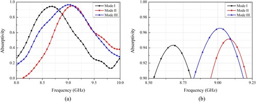
(a) shows the measured absorptivity for all three modes. The results showed a peak absorptivity of 94.3% at 8.68 GHz in Mode I and 95.2% at 9.12 GHz in Mode II. Moreover, a peak absorptivity of 96.9% was observed at 9.02 GHz in Mode III. As shown in (b), the EMA not only changes the operating frequencies but also alters the bandwidth. The bandwidth of absorptivity over 90% in Mode I is 260 MHz, from 8.54 to 8.8 GHz. The bandwidth in Mode II is also 260 MHz, from 8.95 to 9.21 GHz. However, the bandwidth in Mode III is 350 MHz, from 8.83 to 9.18 GHz.
Figure 11. Measurement results in three modes: (a) absorptivity of the proposed EMA and (b) bandwidths of absorptivity over 90%.
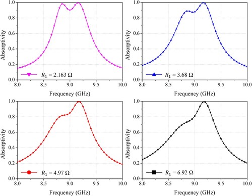
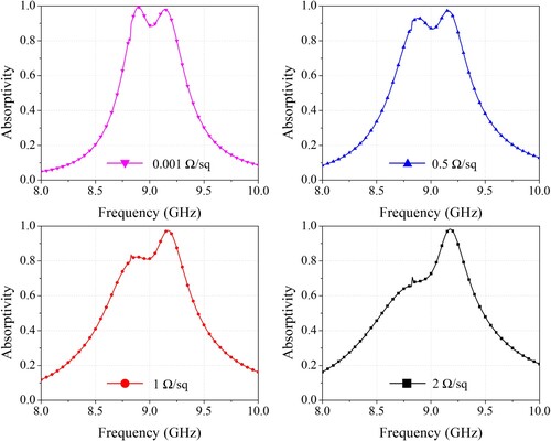
There are discrepancies between the simulation and measurement results in Mode III, particularly regarding the number of peaks observed. In simulation, silver was assigned for the conductive pattern, leading to two distinct peaks in the simulated absorptivity due to the effect of the highly conductive patterns. However, in our fabricated sample, the conductivity may vary for each unit cell, and it is relatively low overall because silver paste was manually applied to the 3D-printed surfaces, which suffers from a rough finishing. As a result, the measured absorptivity showed only one peak, with another peak suppressed due to the low conductivity.
To validate the effect, we simulated the equivalent circuit and gradually increased the value of ((b)) from 2.169 Ω to 6.92 Ω to decrease the conductivity. As shown in , we finally obtained an absorptivity with a single peak similar to the measured absorptivity.
Figure 12. Absorptivity of the equivalent circuit simulation for increasing .
Moreover, we conducted a full-wave simulation to demonstrate the error. To mimic the degraded conductivity, an impedance boundary is applied to the conductive pattern of original geometry and gradually increased from 0.001 Ω/sq to 2 Ω/sq, while the conductive pattern of deformed geometry is applied with silver. Similarly, an absorptivity with a single peak is observed as depicted in .
Figure 13. Absorptivity of the full-wave simulation using impedance boundary applied to the conductive pattern of original geometry.
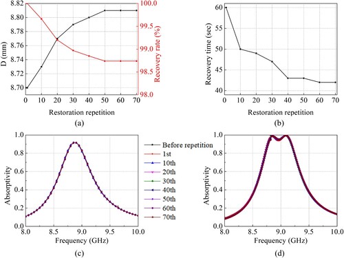
4.2. Deformation and restoration performance
Because geometrical recovery is important, the repeatability test is conducted by measuring the distances between the HT frames (D) after returning to their original states, as shown in . It is observed from (a) that D gradually changes from 8.7 to 8.81 mm up to the 50th repetition. After the 50th repetition, D does not change. The recovery rate is also plotted in (a) and is defined as follows.
(3)
(3) The recovery rate decreases from 100% to 98.74% as D changes. In the meantime, the recovery time in terms of restoration repetition is also presented in (b). Initially, it took 60 s for the structure to recover to the original geometry after the 1st repetition. With multiple restoration repetitions, the recovery time tends to decrease and stabilises at 42 s after 60th repetition. As a result, simulations are conducted to examine how the deviation in D affects the performance of the EMA. As shown in (c,d), both Modes I and III are simulated because Mode III is composed of the unit cells in original states (Mode I). The simulated results show that the geometrical deviation generated from D does not significantly affect the absorption frequency.
Figure 14. Repeatability of the fabricated structure of the EMA: (a) measured D and recovery rate with respect to restoration repetition, (b) recovery time for each repetition, (c) corresponding simulated absorptivity for Mode I and (d) Mode III.
5. Conclusion
In this paper, a frequency – and bandwidth-controllable EMA using 3D-printed SMMWs is proposed. Unlike other works with two states, this EMA has three different modes because we can achieve an independent thermal control of each column. Three modes We used multi-material additive manufacturing to fabricate thermally deformable SMMWs along with SMP and HT filaments for stable deformation. Silver paste was applied on the SMP of SMMWs, and they were assembled on an FR4 plate covered with copper on top. All three modes were numerically and experimentally verified after calculating the equivalent circuit of the EMA. In Mode I, a peak absorptivity of 94.3% at 8.68 GHz and bandwidth of absorptivity over 90% from 8.95 to 9.21 GHz were achieved. In Mode II, a peak absorptivity of 95.2% at 9.12 GHz and a bandwidth of absorptivity over 90% from 8.54 to 8.8 GHz were achieved. Remarkably, in Mode III, a peak absorptivity of 96.9% at 9.02 GHz and a bandwidth of absorptivity over 90% from 8.83 to 9.18 GHz were achieved. Additionally, the repeatability of the EMA was tested through 70 cycles of restoration repetition. We observed trivial variation in the distance between two HT frames, as the absorptivity and operating frequency remained consistent.
Author information
Sungjoon Lim − School of Electrical and Electronic Engineering, Chung-Ang University, 06974 Seoul, Republic of Korea; orcid.org/0000-0002-5049-9300; Phone: + 82-2-820-5827; Email: [email protected]; Fax: + 82-2-812-7431.
Kyounghwan Kim – Department of Intelligent Semiconductor Engineering, Chung-Ang University, Seoul 06974, Republic of Korea
Yelim Kim – School of Electrical and Electronics Engineering, Chung-Ang University, Seoul 06974, Republic of Korea.
Eiyong Park – School of Electrical and Electronics Engineering, Chung-Ang University, Seoul 06974, Republic of Korea.
Heijun Jeong – Department of Electrical and Computer Engineering, University of Delaware, Newark, DE 19716, USA.
Acknowledgment
This research was supported by the National Research Foundation of Korea (NRF) grant funded by the Korea government (MSIT) (2021R1A2C3005239), the MSIT (Ministry of Science and ICT), Korea, under the ITRC (Information Technology Research Center) support program (IITP-2023-RS-2022-00156353) supervised by the IITP (Institute for Information & Communications Technology Planning & Evaluation) and the Chung-Ang University Graduate Research Scholarship in 2021.
Disclosure statement
No potential conflict of interest was reported by the author(s).
Data availability statement
The authors confirm that the data supporting the findings of this study are available within the article and its supplementary materials.
Additional information
Funding
References
- Bhattacharyya S, Srivastava KV. Triple band polarization-independent ultra-thin metamaterial absorber using electric field-driven LC resonator. J Appl Phys. 2014;115(6):064508. doi:10.1063/1.4865273
- Cheng Y, Yang H, Cheng Z, et al. Perfect metamaterial absorber based on a split-ring-cross resonator. Appl Phys A: Mater Sci Process. 2011;102(1):99–103. doi:10.1007/s00339-010-6022-4
- Ghosh S, Lim S. Perforated lightweight broadband metamaterial absorber based on 3-D printed honeycomb. IEEE Antennas Wirel Propag Lett. 2018a;17(12):2379–2383. doi:10.1109/LAWP.2018.2876023
- Landy NI, Sajuyigbe S, Mock JJ, et al. Perfect metamaterial absorber. Phys Rev Lett. 2008;100(20):1–4. doi:10.1103/PhysRevLett.100.207402
- Li H, Hua Yuan L, Zhou B, et al. Ultrathin multiband gigahertz metamaterial absorbers. J Appl Phys. 2011;110(1):014909. doi:10.1063/1.3608246
- Li W, Cheng Y. Dual-Band tunable terahertz perfect metamaterial absorber based on strontium titanate (STO) resonator structure. Opt Commun. 2020;462(October 2019):125265. doi:10.1016/j.optcom.2020.125265
- Park JW, Van Tuong P, Yull Rhee J, et al. Multi-Band metamaterial absorber based on the arrangement of donut-type resonators. Opt Express. 2013;21(8):9691), doi:10.1364/OE.21.009691
- Patel SK, Parmar J, Katkar V, et al. Ultra-Broadband and polarization-insensitive metasurface absorber with behavior prediction using machine learning. Alex Eng J. 2022;61(12):10379–10393. doi:10.1016/j.aej.2022.03.080
- Yang Z, Liang Q, Duan Y, et al. An ultrabroadband metamaterial absorber based on remarkable magnetic coupling via constructing conductive composite resonators and magnetic gradient gyroid structure. Virtual Phys Prototyp. 2023;18(1). doi:10.1080/17452759.2023.2262445
- Yoo M, Lim S. Polarization-Independent and ultrawideband metamaterial absorber using a hexagonal artificial impedance surface and a resistor-capacitor layer. IEEE Trans Antennas Propag. 2014;62(5):2652–2658. doi:10.1109/TAP.2014.2308511
- Zhang T, Li D, Yang Z, et al. A multi-materials 3D-printed continuous conductive fibre-based metamaterial for broadband microwave absorption. Virtual Phys Prototyp. 2024;19(1). doi:10.1080/17452759.2023.2285417
- Kim YJ, Yoo YJ, Hwang JS, et al. Ultra-Broadband microwave metamaterial absorber based on resistive sheets. J Opt. 2017;19(1):015103), doi:10.1088/2040-8986/19/1/015103
- Sheokand H, Ghosh S, Singh G, et al. Transparent broadband metamaterial absorber based on resistive films. J Appl Phys. 2017;122(10):105105. doi:10.1063/1.5001511
- Sun L, Cheng H, Zhou Y, et al. Broadband metamaterial absorber based on coupling resistive frequency selective surface. Opt Express. 2012;20(4):4675. doi:10.1364/OE.20.004675
- Chen X, Li Y, Fu Y, et al. Design and analysis of lumped resistor loaded metamaterial absorber with transmission band. Opt Express. 2012;20(27):28347. doi:10.1364/OE.20.028347
- Nguyen TT, Lim S. Angle- and polarization-insensitive broadband metamaterial absorber using resistive fan-shaped resonators. Appl Phys Lett. 2018a;112(2):021605. doi:10.1063/1.5004211
- Nguyen TT, Lim S. Design of metamaterial absorber using eight-resistive-Arm cell for simultaneous broadband and wide-incidence-angle absorption. Sci Rep. 2018b;8(1):1–10. doi:10.1038/s41598-018-25074-8
- Chaudhary G, Jeong Y. A tunable bandpass filter with arbitrarily terminated port impedance using dual-mode resonator. J Electromagn Eng Sci. 2022;22(6):647–655. doi:10.26866/jees.2022.6.r.134
- Fang J, Huang J, Gou Y, et al. Research on broadband tunable metamaterial absorber based on PIN diode. Optik (Stuttg). 2020;200(February 2019):163171. doi:10.1016/j.ijleo.2019.163171
- Jeong H, Lim S. Broadband frequency-reconfigurable metamaterial absorber using switchable ground plane. Sci Rep. 2018;8(1):1–9. doi:10.1038/s41598-018-27609-5
- Kim HK, Lee D, Lim S. Frequency-Tunable metamaterial absorber using a varactor-loaded fishnet-like resonator. Appl Opt. 2016a;55(15):4113. doi:10.1364/AO.55.004113
- Rana B, Lee IG, Hong IP. Experimental characterization of 2 × 2 electronically reconfigurable 1 Bit unit cells for a beamforming transmitarray at X band. J Electromagn Eng Sci. 2021;21(2):153–160. doi:10.26866/jees.2021.21.2.153
- Xu W, Sonkusale S. Microwave diode switchable metamaterial reflector/absorber. Appl Phys Lett. 2013;103(3):031902), doi:10.1063/1.4813750
- Zhao J, Cheng Q, Chen J, et al. A tunable metamaterial absorber using varactor diodes. New J Phys. 2013;15:043049), doi:10.1088/1367-2630/15/4/043049
- Zhu B, Huang C, Feng Y, et al. Dual band switchable metamaterial electromagnetic absorber. Prog Electromagn Res B. 2010;24(July):121–129.
- Jeong H, Cui Y, Tentzeris MM, et al. Hybrid (3D and inkjet) printed electromagnetic pressure sensor using metamaterial absorber. Addit Manuf. 2020;35(June):101405. doi:10.1016/j.addma.2020.101405
- Le DH, Xu Y, Tentzeris MM, et al. Transformation from 2D meta-pixel to 3D meta-pixel using auxetic kirigami for programmable multifunctional electromagnetic response. Extreme Mech Lett. 2020;36:100670. doi:10.1016/j.eml.2020.100670
- Le DH, Jeong H, Pham TL, et al. A rotary transformable kirigami-inspired metasurface for broadband electromagnetic absorption using additive manufacturing technology. Smart Mater Struct. 2021;30(7):075002. doi:10.1088/1361-665X/abfb81
- Zhang F, Feng S, Qiu K, et al. Mechanically stretchable and tunable metamaterial absorber. Appl Phys Lett. 2015;106(9):091907. doi:10.1063/1.4914502
- Kim J, Jeong H, Lim S. Mechanically actuated frequency reconfigurable metamaterial absorber. Sens Actuators A Phys. 2019;299:111619), doi:10.1016/j.sna.2019.111619
- Ghosh S, Lim S. Fluidically switchable metasurface for wide spectrum absorption. Sci Rep. 2018b;8(1):1–9. doi:10.1038/s41598-018-28574-9
- Kim HK, Lee D, Lim S. A fluidically tunable metasurface absorber for flexible large-scale wireless ethanol sensor applications. Sensors. 2016b;16(8):1246), doi:10.3390/s16081246
- Lim D, Lim S. Liquid-metal-fluidically switchable metasurface for broadband and polarization-insensitive absorption. IEEE Access. 2018;6:40854–40859. doi:10.1109/ACCESS.2018.2857472
- Phon R, Lee M, Kim Y, et al. Thermally reconfigurable helical shape memory alloy–based metamaterial. Electron Lett. 2022;58(1):8–9. doi:10.1049/ell2.12351
- Zhang K, Ma T, Liu J, et al. Dynamically tunable and polarization-insensitive dual-band terahertz metamaterial absorber based on TiNi shape memory alloy films. Results Phys. 2021;23(February):104001. doi:10.1016/j.rinp.2021.104001
- Behl M, Lendlein A. Shape-memory polymers. Mater Today. 2007;10(4):20–28. doi:10.1016/S1369-7021(07)70047-0
- Lendlein A, Kelch S. Shape-Memory effect from permanent shape. Angew Chem, Int Ed Engl. 2002;41:2034–2057.
- Kim Y, Phon R, Jeong H, et al. Management of validation of HPLC method for determination of acetylsalicylic acid impurities in a new pharmaceutical product. Sci Rep. 2022;12(1):1–7. doi:10.1038/s41598-021-99269-x
- Chatham CA, Long TE, Williams CB. A review of the process physics and material screening methods for polymer powder Bed fusion additive manufacturing. Prog Polym Sci. 2019;93:68–95. doi:10.1016/j.progpolymsci.2019.03.003
- Martin AA, Calta NP, Khairallah SA, et al. Double-slit photoelectron interference in strong-field ionization of the neon dimer. Nat Commun. 2019;10(1):1–10. doi:10.1038/s41467-019-10009-2
- Snow Z, Nassar AR, Reutzel EW. Invited Review Article: Review of the Formation and Impact of Flaws in Powder Bed Fusion Additive Manufacturing. Addit Manuf. 2020;36(January):101457. doi:10.1016/j.addma.2020.101457
- Nohut S, Schwentenwein M. Vat photopolymerization additive manufacturing of functionally graded materials: A review. Journal of Manufacturing and Materials Processing. 2022;6(1):17. doi:10.3390/jmmp6010017
- Straathof MH, van Driel CA, van Lingen JNJ, et al. Development of propellant compositions for Vat photopolymerization additive manufacturing. Propellants, Explos, Pyrotech. 2020;45(1):36–52. doi:10.1002/prep.201900176
- Dizon JRC, Espera AH, Chen Q, et al. Mechanical characterization of 3D-printed polymers. Addit Manuf. 2018;20:44–67. doi:10.1016/j.addma.2017.12.002
- Webbe Kerekes T, Lim H, Joe WY, et al. Characterization of process–deformation/damage property relationship of fused deposition modeling (FDM) 3D-printed specimens. Addit Manuf. 2019;25(December 2018):532–544. doi:10.1016/j.addma.2018.11.008
- Shahrubudin N, Lee TC, Ramlan R. An overview on 3D printing technology: technological, materials, and applications. Procedia Manuf. 2019;35:1286–1296. doi:10.1016/j.promfg.2019.06.089
- Nguyen TT, Lim S. Ror2 signaling regulates Golgi structure and transport through IFT20 for tumor invasiveness. Sci Rep. 2017;7(1):1–11. doi:10.1038/s41598-016-0028-x
- Jeong H, Park E, Lim S. Frequency memorizing shape morphing microstrip monopole antenna using hybrid programmable 3-dimensional printing. Addit Manuf. 2022;58(October):102988. doi:10.1016/j.addma.2022.102988
- Park S, Park E, Lee M, et al. Shape-Morphing antenna array by 4D-printed multimaterial miura origami. ACS Appl Mater Interfaces. 2023;15(42):49843–49853. doi:10.1021/acsami.3c11425