Abstract
In this work, we have investigated the effect of Ti nanoparticles (NPs) decoration on the photoluminescence (PL) and photodetection behaviour of ZnO nanowires (NWs) array. ZnO/Ti NW heterostructure was fabricated by synthesising dense NW arrays by uniform decoration of Ti NPs of two different sizes on the surface of the vertically aligned ZnO NWs. The PL spectra shows systematic enhancement (four to six folds) in the UV PL intensity, and also shows corresponding changes in the visible emission with reference to the bare ZnO NWs. We found a major improvement in the photocurrent (PC) and a much faster photoresponse from the ZnO/Ti NW heterostructure. Our studies show that when the thickness of the Ti metal layer is doubled, further improvement in the PC and photoresponse time is obtained from the ZnO/Ti NW heterostructure. The enhancement in the PL and PC are explained on the basis of interfacial charge transfer between Ti NPs and ZnO NWs.
1. Introduction
Due to the unique chemical and physical properties, ZnO nanowires (NWs) arrays have found innovative applications in a variety of applications ranging from field effect transistors, nanolasers to UV photodetectors Citation1–6. Large surface-to-volume ratio and direct carrier conduction path in the NWs makes ZnO NWs a very important nanostructure for the use in nanoelectronic devices. As the surface-to-volume ratio in NWs is very high, the surface states play a key role on optical absorption, luminescence, photodetection and other properties. It is considered that heterostructures are superior for the modulation of selective properties of that material. Using suitable external materials for the heterostructures, one can modify the properties of the material according to its requirements Citation7–9. ZnO NWs covered with dense and uniform ultra small metal nanoparticles (NPs) is one important class of heterostructures. Using suitable noble metal or low work function metal one could achieve very intense UV photoluminescence (PL) and very high photocurrent (PC) along with a significant reduction in the visible emission, which is one of the most important requirements for the application in UV LEDs or photodetectors. Lin et al. Citation10 and Cheng et al. Citation11 reported on the significant enhancement of UV PL intensity and subsequent reduction in the defect-related visible emission from the ZnO NWs covered with ultra small Au NPs. It was reported that beyond certain size of the Au NPs, the UV PL intensity starts decreasing. They proposed that the obtained enhancement is due to the defect loss along with the localised surface Plasmon assisted recombination. On the other hand, when the NWs surface is covered with Ag NPs, a significant improvement in the yellow–green light emission is obtained Citation12. Interestingly, it was reported that NWs covered with some metal leads to a decrease in the PL intensity Citation13. Recently, we have shown that the contact formation between metal NPs and the surface of the ZnO NWs affects the PL and PC behaviours Citation14. Therefore, it would be interesting to study the effect of Ti NP decoration on PL and PC properties, specially the interfacial interaction of the electrons on the photoinduced charge transport mechanism.
In this work, we have fabricated the ZnO/Ti heterostructure and investigated the effect of Ti NPs decoration on the PL and photodetection properties. Ti NPs with two different sizes are decorated on the surface of the ZnO NWs. The PL spectra shows major enhancement in the UV PL intensity, whereas the PC is one order of magnitude higher than the PC of the as-grown case. The enhancement in the PL and PC is explained on the basis of interfacial charge transfer between Ti NPs and ZnO NWs.
2. Experimental details
For the aqueous chemical growth of ZnO NWs, uniform distribution of ZnO nanocrystal seeds were prepared on the Si substrate by thermal decomposition of a zinc acetate precursor. First, 20 mM zinc acetate [(CH3COO)2Zn] solution in ethanol was uniformly coated on the Si substrate. Then the coated substrate was heated at 350°C for 30 min to get ZnO seed layer. The well-aligned ZnO NWs were synthesised by hydrolysis of zinc nitrate [Zn(NO3)2] in water in the presence of hexamethylenetetramine (HMT) on the substrate with seed layer. In this case, Zn(NO3)2 provides Zn2+ ions required for building up ZnO NWs and HMT guide the growth direction. The above prepared substrate is dipped in to a mixture of equimolar (25 mM) concentration of zinc nitrate and HMT in DI–water. The chemical reaction was carried out at 90°C for 1 hour in an autoclave. The substrate was then removed from the solution, rinsed in DI–water and dried in air. The morphology and crystal structure of the as-grown ZnO NWs were characterised using field emission scanning electron microscope (FESEM, Sigma, Zeiss) and X-ray diffractometer (Seifert, 3003 T/T). For the fabrication of heterostructures, Ti NPs were deposited on the surface of the NWs by sputter deposition process for the time duration of 75 s and 150 s. The samples are named as ZnO/Ti1 and ZnO/Ti2 for the Ti deposition time of 75 s and 150 s, respectively. The formation of ZnO/Ti NW heterostructure was confirmed by high resolution transmission electron microscopy (HRTEM, JEM2100, JEOL). The approximate thickness of the Ti layers calculated from the Ti deposition rate was 5 nm and 10 nm, respectively. The exact thickness of the metal layers in each case may vary depending on the orientation of the NWs on the substrate. The sizes of the NPs are slightly larger or comparable to the approximate thickness of the Ti layer. The actual sizes of the Ti NPs are measured from HRTEM imaging. The PL spectra of all the samples were recorded with a 325 nm He–Cd laser excitation using a high-resolution commercial PL spectrometer (FS 920P, Edinburgh Instruments). For comparative analysis, PL measurements on all the samples were made under identical experimental conditions.
For the PC measurements, two circular Al contacts of 100 nm thickness were made on the top of the NWs by thermal evaporation process using a shadow mask. The diameter of the circular electrodes is ∼350 µm with a fixed separation of 2.5 mm between the electrodes. The photoresponse was measured using a picoammeter (Keithley, Model 6487) at a bias of 3 V under the illumination of monochromated UV light (wavelength 365 nm) from a 150 W xenon lamp at a light intensity of ∼0.5 mW/cm2 in ON and OFF conditions. The UV light is focused on the sample making sure that only the region between the two electrodes is illuminated. All the measurements were carried out at room temperature and atmospheric pressure.
3. Results and discussion
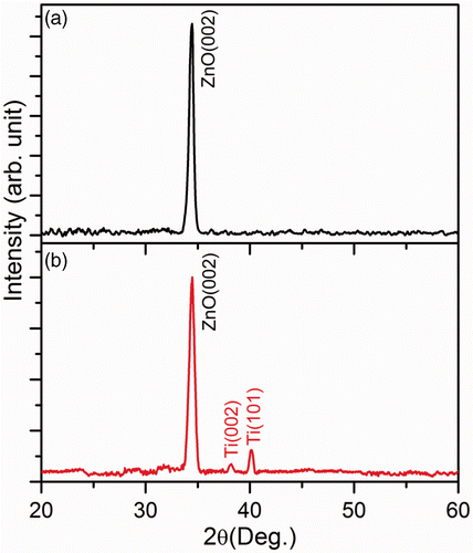
shows the well-aligned growth of ZnO NWs on the Si substrate by aqueous chemical method with the help of ZnO seed layer. As seen from the images, high-density ZnO NWs grew vertically on the substrate over a large area and formed an array like structure. The diameters of the NWs are very small in the range 30–40 nm and the length is about a few microns. During the chemical growth process, ZnO NWs preferentially nucleate from the tip near the grain boundaries between two adjacent grains in the ZnO seed film Citation15. The diameter of the as-grown NWs usually depends on the grain size of the ZnO seeds. The degree of alignment in the as-grown ZnO NWs is strongly controlled by the orientation of the ZnO seed layer. shows the TEM image of the ZnO/Ti1 NWs sample after Ti NPs deposition for 75 s. It is seen that the NPs are distributed on the top as well as the side surface of the NWs. Due to the NPs decoration, the diameter of the above NW is found to be larger than that of the bare ZnO NWs. shows a magnified view of the Ti NPs decoration. The sizes of the Ti NPs vary in the range 4–6 nm. To study further about the structure of the NWs, we performed XRD measurements of the as-grown and ZnO/Ti2 NWs. The XRD result is shown in , which shows a strong peak at 34.45° corresponding to (002) planes of ZnO. The observed strong peak indicates the highly crystalline nature of the as-grown NWs with growth orientation along the c-axis of hexagonal structure of ZnO. Along with the (002) peak of ZnO crystal, the ZnO/Ti2 heterostructure shows additional peaks corresponding to the (002) and (101) lattice planes of Ti nanocrystals. Therefore, the XRD pattern of the ZnO/Ti2 heterostructure confirmed that the Ti is present in a metallic phase in the heterostructure and that no other form, e.g. TiO2, is produced during the deposition.
Figure 1. FESEM images of the chemically grown ZnO NWs on Si substrate: (a) top view, (b) 45° tilted view, (c) TEM image of the ZnO/Ti NW heterostructure, where the Ti was deposited for 75 s, (d) a magnified side view of the above heterostructure. Both the images clearly show the decoration of the Ti NPs (marked by solid arrow) on the surface of the ZnO NWs.
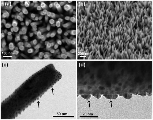
Figure 2. XRD patterns of the chemically grown NWs: (a) as-grown ZnO NWs and (b) ZnO/Ti2 NWs heterostructure, respectively.
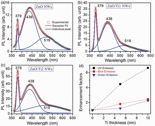
The room temperature PL spectra of the as-grown and ZnO/Ti NW heterostructures are shown in . The as-grown NWs exhibit near band edge (NBE) UV emission at 379 nm and a broad visible emission band in the blue–green region. Gaussian multipeak fitting shows the existence of two emission bands, one at the blue region centred at ∼436 nm and another at the green region centred at 519 nm. The observed NBE emission is due to free excitonic recombination while the blue and green emission bands are due to the presence of interstitial zinc (Zn
i
) Citation16 and single ionised oxygen vacancy () Citation17, respectively. The strong blue peak indicates the formation of dense interstitial zinc states in the as-grown ZnO NWs. It is known that, in the aqueous chemical method, zinc nitrate provides Zn2+ ions whereas the H2O supplies the OH− ions required for the oxidation of Zn2+ ions. Due to the comparatively faster rate of hydrolysis of zinc nitrate than the H2O, formation of high density of interstitial zinc in the as-grown NWs is expected. After the Ti NPs decoration, the UV peak intensity is dramatically enhanced, while the intensity of blue and green emissions are relatively less enhanced. The enhancement factors of these three emissions gradually increase with the increase in Ti NPs thickness/diameter. The UV PL intensity is enhanced by a factor of 4.5 for ZnO/Ti1 heterostructure and 6.6 for ZnO/Ti2 heterostructure whereas the enhancement factors for the blue and green emissions are in the range of 1.5–2.4. Therefore, the UV emission of the ZnO NWs is strongly influenced by the Ti NPs and it shows further improvement with higher thickness of Ti NPs. An earlier report shows a similar improvement in the PL intensity from the Ti doped ZnO NWs obtained by Ti plasma immersion ion implantation method Citation18. It is expected that the above ZnO/Ti heterostructures will exhibit similar improvement in the PC and photoresponse behaviour.
Figure 3. Room temperature PL spectra of the: (a) as-grown ZnO NWs, (b) ZnO/Ti1 NWs heterostructure and (c) ZnO/Ti2 NWs heterostructure, respectively. A significant improvement in the intensity of the UV PL is obtained after the deposition of Ti NPs on the ZnO NWs. Three peaks are fitted with Gaussian line shape functions (solid line) to the experimental data (open circle). (d) Variations of enhancement factors of UV, blue and green emissions with different thickness of Ti.
The obtained enhancement in the PL spectra from the ZnO/Ti heterostructure can be explained as follows. It is known that when a metal is brought in contact with a semiconductor, it induces band bending due to the equilibrium of Fermi level. Depending on the difference in the work functions of metal and semiconductor, two types of contacts may form at the metal semiconductor interface. Since the work function of ZnO (4.65 eV) Citation19 is larger than the Ti (4.26 eV) Citation20, an Ohmic contact is formed with downward band bending, which is shown schematically as an inset in . This will facilitate the electron transfer process from Ti to the conduction band of ZnO and electron accumulation on the surface/interface will increase substantially. Therefore, even if the photon-generated electron–hole pairs are separated at the interface, the radiative recombination probability of electrons on the conduction band and holes in the valence band/defect level will increase dramatically due to replenishment of electrons from Ti. As a result, both the UV and green emissions intensities increase with Ti coverage.
Figure 4. Dark current–voltage characteristics of the as-grown ZnO NWs and ZnO/Ti2 NWs heterostructure. Inset shows the energy band alignment of the above heterostructure. The solid arrow mark shows the easy transfer of electrons from the Fermi level of Ti to the conduction band of ZnO NWs, resulting in larger dark current.
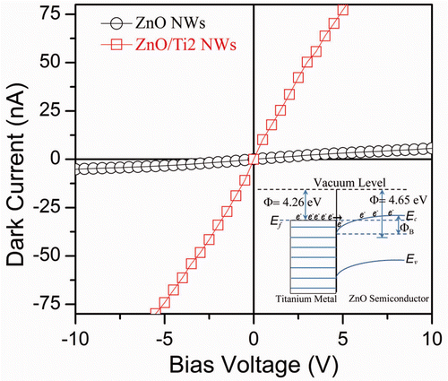
shows the dark current–voltage (I–V) characteristics of the as-grown NWs and ZnO/Ti heterostructure. The I–V characteristics show nearly linear behaviours with current in the range of nA. The ZnO/Ti2 heterostructure shows a dramatic increase in the dark current as compared to the as-grown NWs. The dark current increases to 50 nA from 2 nA at a bias of 3 V after the decoration of the Ti NPs. The ZnO/Ti1 heterostructure also shows high dark current with a current of 18 nA. As explained before, due to the downward band bending at the interface between Ti NPs and ZnO NWs, more numbers of electrons can easily transfer from Ti to the conduction band of ZnO. Under the bias, these electrons will contribute to the current conduction process resulting in a high dark current. In the ZnO/Ti2 heterostructure, due to higher thickness of Ti layer, more number of electrons can flow to the ZnO causing a systematic increase in dark current with increase in Ti coverage.
The photoresponse of the as-grown and ZnO/Ti heterostructures are measured under the UV light (wavelength 365 nm) pulse in ON and OFF conditions and the results are shown in . The PC initially grows very fast, then increases slowly with time and finally saturates. Similarly, during the decay process the PC initially decreases very rapidly and then slowly reaches the dark current value. From the transient PC behaviours it is revealed that the ZnO/Ti NW heterostructures give a maximum photo-generated current, ΔI max (PC minus dark current) of 20.43 µA for the ZnO/Ti1 heterostructure and 51.65 µA for the ZnO/Ti2 heterostructure, respectively. Therefore, for the ZnO/Ti2 heterostructure ΔI max is one order of magnitude higher than the case of as-grown NWs (4.92 µA). The time-dependent PC growth and decay curves are fitted with the following equation,
Figure 5. Photoresponse behaviors (measured at 365 nm) of the: (a) as-grown ZnO NWs, (b) ZnO/Ti1 NWs heterostructure and (c) ZnO/Ti2 NWs heterostructure, respectively, measured at a bias voltage of 3 V. The photocurrent is measured under UV light in ‘ON’ and OFF conditions. Individual growth and decay time constants are calculated from the modified bi-exponential fitting (solid line) to the experimental data points (open circle). (d) Change in time constants (1st and 2nd components of PC growth) with the thickness of Ti metal layer.
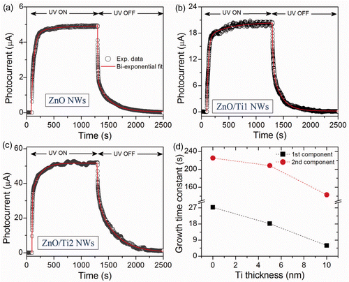
To explain the faster photoresponse from the ZnO/Ti NWs heterostructure, first we need to understand the involvement of oxygen adsorption and photodesorption processes in the photoresponse of ZnO. Adsorption of oxygen molecules at the vacant sites on the surface of the ZnO NWs leads to a decrease in conductivity Citation22,Citation23. Under the UV irradiation, electron–hole pairs are generated that increase the photocurrent, and oxygen molecules are released by photodesorption process. At the same time, some of the released oxygen molecules are re-adsorbed and it decreases the photocarriers. As a result, a steady photocurrent value is obtained after certain time. When the UV light is OFF, the electron–hole pair recombination and adsorption processes dominate and the photocurrent value reaches the initial value after a certain time of decay. Therefore, the fast or slow response strongly depends on the time taken to reach the equilibrium of oxygen desorption and re-adsorption processes. In the present case, the decoration of Ti NPs induces rough surface morphology and large numbers of interface states between Ti and ZnO, which results in surface modification. We believe that, these interface traps improve the photoresponse process, resulting in comparatively faster photoresponse process.
4. Conclusion
In summary, ZnO/Ti NWs heterostructure was fabricated by depositing small sizes of Ti NPs with different sizes on the surface of the chemically grown ZnO NWs and the resulting improvement in the PL and photodetection properties was investigated. The PL spectra shows a major enhancement (four to six fold) in the UV PL intensity and relatively small increment in the visible emission intensity. The PC of the ZnO/Ti NW heterostructure also shows large improvement, as compared to the case of bare ZnO NWs. The enhancement in the PL and PC are explained on the basis of interfacial charge transfer between Ti NPs and ZnO NWs. In the heterostructure case, a large number of electrons are easily transferred to the conduction band of ZnO through the interface between Ti NPs and ZnO due to the downward band bending in the ZnO. The photoresponse time is also significantly reduced for the ZnO/Ti heterostructure due to the faster relaxation of charge carriers through the rough surface induced traps. Our studies show that the higher thickness of the Ti metal results into higher improvement in the UV PL and faster photoresponse from the ZnO/Ti heterostructure.
References
- Sakurai , M , Wang , Y G , Uemura , T and Aono , M . 2009 . Electrical properties of individual ZnO nanowires . Nanotechnology , 20 Article ID 155203 doi: 10.1088/0957-4484/20/15/155203
- Yang , H Y , Lau , S P , Yu , S F and Abiyas , A P . 2006 . High temperature random lasing in ZnO nanowires . Phys. Rev. Lett. , 89 Article ID 011103
- Wei , A , Pan , L and Huang , W . 2011 . Recent progress in the ZnO nanostructure-based sensors . Mat. Sci. Eng. B , 176 : 1409 – 1421 . doi: 10.1016/j.mseb.2011.09.005
- Vj , L , Oh , J , Nayak , A P , Katzenmeyer , A M , Gilchrist , K H , Grego , S , Kobayashi , N P , Wang , S-Y , Talin , A A , Dhar , N K and Islam , M S . 2011 . A perspective on nanowire photodetectors: Current status, future challenges, and opportunities . IEEE J. Sel. Top. Quantum Electron. , 17 : 1002 – 1032 . doi: 10.1109/JSTQE.2010.2093508
- Kumar , N , Dorfman , A and Hahm , J-I . 2006 . Ultrasensitive DNA sequence detection using nanoscale ZnO sensor arrays . Nanotechnology , 17 : 2875 – 2881 . doi: 10.1088/0957-4484/17/12/009
- Wei , A , Sun , X W , Wang , J X , Lei , Y , Cai , X P , Li , C M , Dong , Z L and Huang , W . 2006 . Enzymatic glucose biosensor based on ZnO nanorod array grown by hydrothermal decomposition . Appl. Phys. Lett. , 89 Article ID 123902
- Bera , A and Basak , D . 2009 . Photoluminescence and photoconductivity of ZnS-coated ZnO nanowires . ACS Appl. Mater. Interfaces , 2 : 408 – 412 . doi: 10.1021/am900686c
- Dhara , S and Giri , P K . ZnO/anthracene based nanowires heterostructure: Photoresponse and photoluminescence studies, J. Appl. Phys. 111 (2012), Article ID 044320
- Chang , J , Najeeb , C K , Lee , J-H , Lee , M and Kim , J-H . 2011 . High-performance photoresponse from single-walled carbon nanotube–zinc oxide heterojunctions . J. Phys. D: Appl. Phys. , 44 Article ID 095101
- Lin , H Y , Cheng , C L , Chou , Y Y , Huang , L L , Chen , Y F and Tsen , K T . 2006 . Enhancement of band gap emission stimulated by defect loss . Opt. Express , 16 : 2372 – 2379 . doi: 10.1364/OE.14.002372
- Cheng , C W , Sie , E J , Liu , B , Huan , C HA , Sum , T C , Sun , H D and Fan , H J . 2010 . Surface plasmon enhanced band edge luminescence of ZnO nanorods by capping Au nanoparticles . Appl. Phys. Lett. , 96 Article ID 071107
- Lin , C-A , Tsai , D-S , Chen , C-Y and He , J-H . 2011 . Significant enhancement of yellow–green light emission of ZnO nanorod arrays using Ag island films . Nanoscale , 3 : 1195 – 1199 . doi: 10.1039/c0nr00732c
- Fang , Y J , Sha , J , Wang , Z L , Wan , Y T , Xia , W W and Wang , Y W . 2011 . Behind the change of the photoluminescence property of metal-coated ZnO nanowire arrays . Appl. Phys. Lett. , 98 Article ID 033103
- Dhara , S and Giri , P K . 2011 . On the origin of enhanced photoconduction and photoluminescence from Au and Ti nanoparticles decorated ZnO nanowire heterostructures . J. Appl. Phys. , 110 Article ID 124317 doi: 10.1063/1.3671023
- Hsiao , C S , Peng , C H , Chen , S Y and Liou , S C . 2006 . Tunable growth of ZnO nanorods synthesized in aqueous solutions at low temperatures . J. Vac. Sci. Technol. B , 24 : 288 – 291 . doi: 10.1116/1.2163889
- Lin , B , Fu , Z and Jia , Y . 2001 . Green luminescent center in undoped zinc oxide films deposited on silicon substrates . Appl. Phys. Lett. , 79 : 943 – 945 . doi: 10.1063/1.1394173
- Vanheusden , K , Warren , W L , Seager , C H , Tallant , D R , Voigt , J A and Gnade , B E . 1996 . Mechanisms behind green photoluminescence in ZnO phosphor powders . J. Appl. Phys. , 79 : 7983 – 7990 . doi: 10.1063/1.362349
- Liao , L , Zhang , Z , Yang , Y , Yan , B , Cao , H T , Chen , L L , Li , G P , Wu , T , Shen , Z X , Tay , B K , Yu , T and Sun , X W . 2008 . Tunable transport properties of n-type ZnO nanowires by Ti plasma immersion ion implantation . J. Appl. Phys. , 104 Article ID 076104
- Aguilar , C A , Haight , R , Mavrokefalos , A , Korgel , B A and Chen , S . 2009 . Probing electronic properties of molecular engineered zinc oxide nanowires with photoelectron spectroscopy . ACS Nano , 3 : 3057 – 3062 . doi: 10.1021/nn900777k
- Lide , D R . 2009 . CRC Handbook of Chemistry and Physics , CRC : Boca Raton .
- Dhara , S and Giri , P K . 2011 . Enhanced UV photosensitivity from rapid thermal annealed vertically aligned ZnO nanowires . Nanoscale Res. Lett. , 6 Article ID 504
- Li , Q H , Gao , T , Wang , Y G and Wang , T H . 2005 . Adsorption and desorption of oxygen probed from ZnO nanowire films by photocurrent measurements . Appl. Phys. Lett. , 86 Article ID 123117
- Soci , C , Zhang , A , Xiang , B , Dayeh , S A , Aplin , D PR , Park , J , Bao , X Y , Lo , Y H and Wang , D . 2007 . ZnO nanowire UV photodetectors with high internal gain . Nano Lett. , 7 : 1003 – 1009 . doi: 10.1021/nl070111x