Abstract
In this article, nanocrystalline Mg2TiO4 (MTO) thin films were deposited on quartz substrates with a thickness ranging from 200 to 300 nm at ambient temperature by the radio frequency magnetron sputtering method. These films were kept under O2 standard cubic centimeters per minute (SCCM) and, post deposition, annealing in air at 500°C for 1 h. The structure of the sintered target and films were analysed by X-ray diffraction (XRD). The XRD patterns indicated that these films are amorphous structurally, and annealing process induces the formation of crystalline phase. The microstructure and surface morphology of the MTO films were studied by field emission scanning electron microscopy and atomic force microscopy. The post-deposition annealing resulted in an amorphous-crystalline phase transition in the films, which is accompanied by an increase in the refractive index and decrease in the optical bandgap. The annealed films exhibit a refractive index of 1.98–2.03 (at 600 nm) with an optical bandgap values between 4.44 and 4.58 eV. The increase of refractive index for annealed films can be attributed to increase of crystalline nature and packing densities. The O2 SCCM and annealing also greatly affected the photoluminescence spectra. In addition, the characteristic emission sharp peak and shoulder peaks at 357, 409 and 466 nm were detected.
1. Introduction
Modern technology is demanding smart materials with advanced properties to incorporate more and more functions in electronic devices, especially for microwave resonator and communications applications because these materials facilitate miniaturisation to wireless devices Citation1. Among them, dielectric oxides are considered to be one of the best materials for optical thin film applications because they offer various functional properties such as infrared optical sensors, planar wave guides, electro-optic switches and coupling in optical communications Citation2,Citation3. Mg2TiO4 (MTO) is an excellent microwave dielectric material with a wide bandgap and high refractive index suitable for optical and electronic applications. Therefore, its practical applications in optical response are very promissory. Recently, MTO thin films have become important in optical modulation, the protective layer of plasma display panels and in the monolithic microwave integrated circuit technologies. In addition, MTO thin films are useful for high-temperature superconductor (HTSC) substrates because of their high chemical, mechanical and thermal stability properties. Basically, MTO ceramic is used as a novel substrate for HTSC thin films due to its low microwave loss and well-defined surface structure Citation4. In addition, they are capable in reducing the dimension of a device in communication integration density. Moreover, thin film technology has become a major requirement for integration since integrated circuits have been applied in microwave communication systems. Among other spinels, MTO is a most promising dielectric candidates, having the inverse type spinel belonging to cubic structure with space group (Fd-3 m) No 227, exhibits an average dielectric constant (εr) ∼ 14, a high-quality factor (Qƒ0) ∼ 150,000 GHz and a negative temperature coefficient of resonant frequency (τf) ∼ −50 ppm/°C Citation5–8.
Although there are few reports on bulk properties, however, to the best of the authors knowledge, there were no reports on thin films. The structural and optical study of MTO thin films deposited at ambient temperature was studied by Bhuyan et al. Citation9. Hence, it is important to study the dependence of film properties on the deposition conditions especially with O2 standard cubic centimeters per minute (SCCM) and the post-deposition annealing, in order to study their structural and optical properties. On the other hand, optical properties of thin films are known to be very sensitive to defects as well as microstructure variations. Therefore, from spectral transmission behaviour of transparent films on transparent substrates, a wealth of structural, microstructural and optical information can be extracted. Optical properties such as refractive index (n), packing density (p) and optical bandgap (Eg ) are important parameters, which determine the overall optical behaviour of these films.
Therefore, in this article, we investigated the effects of O2 SCCM of the sputtering gas and the annealing on the properties of MTO films. We prepared nanocrystalline MTO films on quartz substrates by using radio frequency (RF) magnetron sputtering with varying O2 SCCM (from 4 to 28 SCCM) during deposition, and all the films were then subjected to post-deposition annealing in air at 500°C for 1 h. The effect of processing parameters and post-deposition annealing on the crystallinity, microstructure and optical properties of MTO thin films has been investigated.
2. Experimental procedure
2.1. Preparation of MTO target
MTO sputtering target was prepared by mechanochemical synthesis method from high-purity oxides (>99.9%) powders: MgO and TiO2. The starting materials were mixed according to the desired stoichiometry ratio, and the powders were ball-milled for 30 h using planetary ball mill (Fritsch GmbH, Germany). After drying and sieving, the powders were uniaxially pressed to produce the MTO target of 50 mm diameter. Then, the sputtering target was sintered at 1350°C for 3 h and cooled to room temperature at 2°C/min cooling rate.
2.2. Characterisation techniques
Crystal structure of the MTO sintered sputtering target and deposited films were analysed by X-ray diffractometer (Bruker D8) using Cu Kα (λ = 1.5406 Å) radiation, and target material was refined by using Rietveld refinement method and with fool-proof software Citation10. Surface morphology of the thin films was studied by using field emission scanning electron microscope (FESEM; Sigma Zeiss). Scanning probe microscope (Seiko Instruments Inc., SPA-400) was used in the contact atomic force microscopy (AFM) mode to obtain images of the surface morphology of the MTO films. Spectral transmission characteristics in the wavelength range 200–1400 nm were measured using a UV-VIS-NIR spectrophotometer (UV 3101PC, Shimdzu). The optical constants have been calculated using the envelope technique Citation11. Photoluminescence (PL) measurements were performed at room temperature through thermo-spectronic (Aminoco-Bowman-2) double monochromator coupled to a GaAs photomultiplier with a conventional photon counting system.
2.3. Optimisation of processing parameters
The deposition of the films was carried out at ambient temperature on quartz substrates, and all the films were then subjected to post-deposition annealing in air at 500°C for 1 h. The base pressure of the chamber was maintained at 10−4 Pa. The process gas was a mixture of high-purity argon (Ar) and oxygen (O2) and introduced to the chamber through mass-flow controllers. The target was pre-sputtered in an argon atmosphere for 10 min to eliminate surface impurities. All the films were deposited at a fixed power of 80 W for 3 h and the sputtering pressure of 38 mTorr. All films were prepared at different oxygen gas pressure in SCCM.
3. Results and discussion
3.1. Characterisation of target material
shows the X-ray diffraction (XRD) patterns of the MTO sputtering target sintered at 1350°C for 3 h along with the Rietveld refinement. XRD pattern of the target material was refined by using Rietveld refinement technique and fool-proof program. The refinement was carried out by varying cell parameters, position of the Mg, Ti, and O atoms occupancy and thermal parameters. The lattice parameters derived from the XRD patterns are found to be a = b = c = 8.4544 (15) Å and bond angles with medium values (α = β = γ = 90°) estimated from the refinement confirmed the cubic structure for this material. The derived data from Rietveld refinement was well set with the standard data of MTO ceramics. The average crystallite size estimated using Scherrer's formula was found to be 40 nm for the target material. There is no evidence of secondary phases observed from the XRD patterns, which show that the processing parameters in the mechanochemical synthesis are optimised. The parameters obtained from the Rietveld analysis of XRD patterns for the MTO target is shown in .
Figure 1. XRD patterns along with Riveted refinement of Mg2TiO4 ceramic target material sintered at 1350°C. The circles and solid line present the experimental and the Rietveld refined data, respectively. The dotted line at the bottom shows the difference between the experimental and the refined data. The vertical bars correspond to the allowed Bragg's peaks.
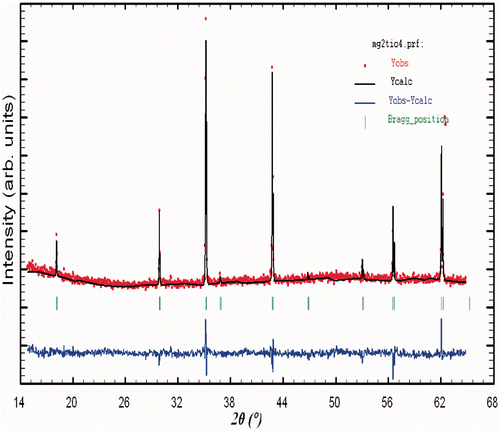
Table 1. Parameters obtained from the Rietveld analysis for MTO target materials sintered at 1350°C. χ 2, R Brag and Rf are reliability factors
3.2. Characterisation of MTO films
3.2.1. Crystallinity and microstructure
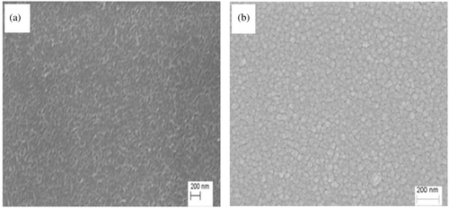
shows the XRD patterns of MTO thin films deposited on quartz substrate at various O2 SCCMs and annealed at 500°C for 1 h. All the as-deposited films were found to be amorphous structurally and become crystalline after the post-deposition annealing. In other words, the presence of diffraction peaks can be used to evaluate the structural order at long range of the material Citation12. It was observed that the MTO (102) and (200) peaks were enhanced gradually with increasing O2 SCCM for annealed films. Moreover, the full width at half maximum intensity values of the MTO (102) and (200) peaks decreased with increasing O2 partial pressure. It indicates that larger sized crystal grains and lower concentration of crystal defects are available in the annealed films. Furthermore, the peak position shifts to higher angle with increasing the O2 SCCM. It is known that the oxide thin films naturally grow in the amorphous state, and the activation energy is given either in the form of temperature or ion bombardment to initiate the crystal growth. The post-deposition annealing at 500°C for 1 h resulted in the development of necks between grains. This mechanism occurs by the grain boundary motion owing to a reduction of the total grain boundary surface energy. The thermal energy leads to an increase in the diffusion rate and consequently intensifies the formation of necks between grains, which was confirmed from (AFM + FESEM) microstructures Citation13. The average crystallite size of the films estimated using Scherrer's formula increases from 9 to 18 nm with an increasing the O2 SCCM. shows the FESEM micrographs of MTO thin films for as-deposited and annealed films deposited at 12 SCCM O2. It is observed that the surface morphology of the as-deposited amorphous MTO film does not show any distinct grain structure, and a few dimples are clearly visible in the surface of the film. Upon annealing, there is an enhancement in the grain growth and the surface becomes smooth, more compact and distinct grains with higher O2 partial pressure. This is in good agreement with the earlier reports Citation14. Significantly, during the annealing process the densification of the films increased along with the decrease of porosity and the later one reflected in the increase of packing density of the films.
Figure 2. XRD patterns of MTO films deposited on quartz substrate at different O2 SCCM for (a) as-deposited films and (b and c) annealed films.
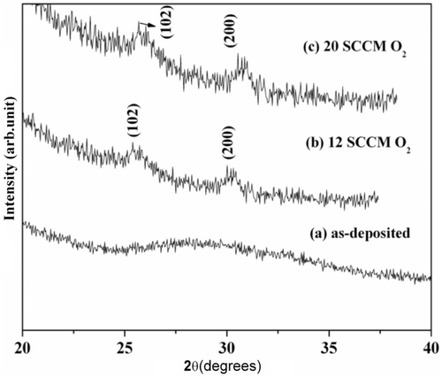
Figure 3. FESEM images of MTO thin films deposited on quartz at 12 SCCM O2 for as-deposited and (b) annealed films.
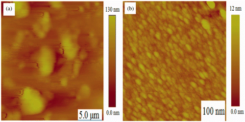
The as-deposited and annealed AFM images of the MTO thin films deposited at 12 O2 SCCM was shown in , respectively. From the AFM images, it is evident that the as-deposited film does not show any apparent grain structure. On the other hand, the AFM images of the annealed films reveal the nano-sized grain morphology with an average grain size of about 40–60 nm after annealing. The AFM morphology also indicates that the annealed film is dense and fine grained having no porosity. This fine micro structured thin film with a higher packing density and smaller roughness is more suitable for various optical applications. The AFM analysis of the MTO thin films is also well consistent with FESEM result.
Figure 4. AFM surface morphology of MTO films deposited on quartz at 12 SCCM O2 for (a) as-deposited and (b) annealed films.
3.2.2. Optical properties
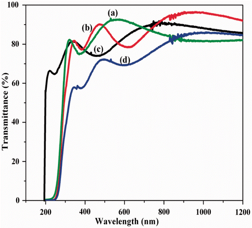
shows the optical transmittance spectra for as-deposited and annealed MTO films, which are deposited on quartz substrates at different O2 SCCM. It is observed that the as-deposited films were more transparent when compared with the annealed films due to the absence of scattering grain boundaries. The sharp fall in transmission and disappearance of fringes at shorter wavelength is due to fundamental absorption of the films. It is revealed that annealed films, which are deposited at higher O2 SCCM show lower transmittance. The reduction in transmittance with increase in O2 SCCM can be attributed to the increase in average crystallite size resulting in higher scattering of light on grain boundaries; upon annealing, the films result in a denser structure having lesser voids. This does not allow the light to pass through and hence the reduction in the transmittance and is also confirmed from FESEM and AFM images.
Figure 5. Optical transmittance spectra of MTO thin films deposited on quartz substrates for as-deposited at (a) 12 SCCM O2 (b) 28 SCCM O2 and annealed films deposited at (c) 12 SCCM O2 (d) 28 SCCM O2.
The refractive index (n) of the film was derived by employing the envelope method Citation11 on the basis of the following expressions,
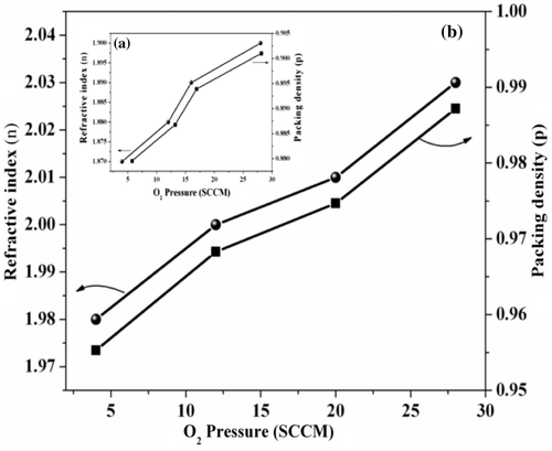
illustrates the variation of refractive index (n 600, λ = 600 nm) and packing density (P) with O2 SCCM for as-deposited (see inset of ) and annealed MTO films. It reveals that annealed films show higher values of refractive index as compared with as-deposited films. For example, for the as-deposited film at 20 SCCM O2, the refractive index is 1.89 (at 600 nm), which increased to 2.01 at the same wavelength for annealed films. It is well known that the refractive index of a transparent thin film is directly proportional to its electronic polarisation, which is inversely proportional to the inter-atomic separation Citation17. It can also be directly correlated to the film packing density, microstructure and crystallinity. It should be noted that in this case, the as-deposited films are highly disorder due to their amorphous nature resulting in lower film density, which in turn results in the lowering of the refractive index. On annealing, there is a reduction in the inter-atomic spacing resulting in the densification of the films (porosity decreases) leading to an increase in the refractive index. Hu et al. Citation18 also reported that increasing packing density would lead to a higher refractive index for the HfO2 films. Furthermore, the observed results suggest that the packing density decreases the bandgap.
Figure 6. Variation of refractive index and packing density as a function of O2 SCCM for (a) as-deposited (inset) and (b) annealed films.
3.2.3. Optical bandgap
The variation in bandgap for the as-deposited and annealed MTO films as a function of O2 SCCM is shown in . The optical bandgap (Eg ) for all the films was calculated using the Tauc relation Citation19, which is given by αhυ = β(hν−Eg ) n , where hν is the photon energy, β is a constant, which is a measure of crystalline order in the deposited films, and n = 0.5, 1.5, 2 or 3 for allowed-direct, forbidden-direct, allowed-indirect and forbidden-indirect electronic transitions, respectively. In this case, the bandgap energy (Eg ) has been estimated by assuming an allowed direct electronic transition between the highest occupied state of the valence band and the lowest unoccupied state of the conduction band. Inset shows the dependence of the absorption coefficients (αhν)2 on photon energy (hν) for the annealed films. The band-gap energy (Eg ), of the films was obtained by extrapolating the linear portion of the plot of (αhν)2 against photon energy (hν) to (αhν)2 = 0.
Figure 7. (a) Variation in bandgap as a function of O2SCCM for the as-deposited and annealed MTO films, (b) Inset shows the dependence of (αhν)2 against photon energy (hν) for the annealed film deposited at 28 SCCM O2.
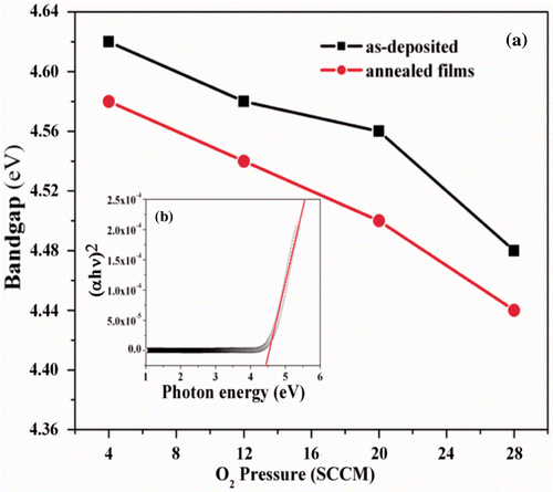
It can be seen that optical bandgap of the annealed films found to decrease with O2 SCCM. The bandgap of the as deposited film was 4.48 eV, which decreases to 4.44 eV for annealed film deposited at 28 SCCM O2. The optical bandgap values are a good qualitative estimation of stoichiometry. The decrease in optical bandgap with annealing may be attributed to the increase of intermediary energy levels within the bandgap. Moreover, the low porosity and increase of packing density caused due to a better crystalline nature. It is well known that when a crystalline phase is embedded in a largely amorphous matrix of film, there are large deviations in optical bandgap of the films from bulk values Citation20.
3.2.4. PL behaviour analysis
illustrates the PL spectra recorded at room temperature for as-deposited and annealed MTO thin films deposited at different O2 SCCM. It is observed that the characteristic emission sharp peak and shoulder peaks at 357, 409 and 466 nm were detected. The PL spectra indicated that the annealed MTO films, which are deposited at higher O2 SCCM exhibited the maximum intensity with a characteristic peak at 357 nm, which corresponds to the intensive UV emission together with two week green emissions. It is noted that after annealing, the intensities of MTO films increases as intensity of the emission peaks strongly depend on the films density. Furthermore, the effect of annealing and the increase of O2 SCCM increase the grain size of the films and hence the ratio of the surface area to volume decreases. As a result, the films become more compact and fewer defects, the number of released photon increases, thus the intensity increases and the line-width decreases.
Figure 8. PL spectra of MTO films deposited at different O2 SCCM for (a and b) as-deposited films and (c–e) annealed film.
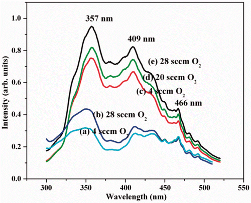
PL results compliment the optical bandgap values that the increase in O2 SCCM results the highest intensity of the peaks, which can be attributed to the high degree of structural order and disorder in to the lattice Citation21. From the bandgap calculations, it is observed that for as-deposited and annealed films bandgap decreases with O2 SCCM. It is known that the order films exhibit lower bandgap values compared to the disorder films. Furthermore the characteristic peak of the films shifted slightly with the increase O2 SCCM due to the grain growth. As observed from transmittance spectra, the highest intensity film exhibited the lowest bandgap. The increase in intensities from PL spectrum and decrease in bandgap can be attributed to the increase of intermediary energy levels within the bandgap due to the defects in clusters of crystalline structure Citation21.
4. Conclusions
In summary, nanocrystalline MTO thin films were deposited on quartz substrates by RF magnetron sputtering. The as-grown films were structurally amorphous and post-deposition annealing was carried out at 500°C for 1 h in air to induce crystallisation. The effects of post-deposition annealing and O2 SCCM on structural, microstructural and optical properties of MTO films studied systematically. It was found that upon annealing, there is an evident of clear transition in the surface features with more compact and distinct grains and was conformed from FESEM and AFM images. When we compared the crystalline with the amorphous films, the amorphous films had higher bandgap and lower refractive index. The variation of refractive index and packing density with O2 SCCM for annealed films is attributed to increase in the optical density with increase in crystalline nature. In addition, intense visible PL emission was observed for MTO thin films, and it was found that the annealed films showed high emission peaks than the as-deposited films. These results indicated that the increase in the grain size and reduction in the ratio of the surface area to the volumes leads to an improvement in PL emission.
Acknowledgements
The authors acknowledge the financial support from DRDO [ERIP/ER/0900371/M/01/1264] and DAE BRNS [2010/20/37 P/14BRNS.], India.
References
- Huang , C L and Ho , C En . 2010 . Microwave dielectric properties of (Mg1−xNix)2TiO4 (x = 0.02–0.1) ceramics . Int. J. Appl. Ceram. Technol. , 7 : E163 – E169 . doi: 10.1111/j.1744-7402.2010.02495.x
- Walker , F J , McKee , R A , Yen , H W and Zelmon , D E . 1994 . Optical clarity and waveguide performance of thin film pervoskites on MgO . Appl. Phys. Lett. , 65 : 1495 – 1497 . doi: 10.1063/1.112023
- Kim , D-Y , Moon , S E , Kim , E-K , Lee , S-J , Choi , J-J and Kim , H E . 2003 . Electro-optic characteristics of (001)-oriented Ba0.6Sr0.4TiO3 thin films . Appl. Phys. Lett. , 82 : 1455 – 1457 . doi: 10.1063/1.1556962
- Haefke , H , Lang , H P , Sum , R , Guntherodt , H J , Berthold , L and Hesse , D . 1992 . Mg2TiO4 as a novel substrate for high temperature superconducting thin films . Appl. Phys. Lett. , 61 : 2359 – 2361 . doi: 10.1063/1.108243
- Takada , T , Wang , S F , Yoshikawa , S , Yang , S J and Newnham , R E . 1994 . Effect of glass additives on BaO-TiO2-WO3 microwave ceramics . J. Am. Ceram. Soc. , 77 : 1909 – 1916 . doi: 10.1111/j.1151-2916.1994.tb07070.x
- Cava , R J , Peck Jr , W F , Krajewski , J J , Reberts , G L and Barber , B P . 1997 . Improvement of the dielectric properties of Ta2O5 through substitution with Al2O3 . Appl. Phys. Lett. , 70 : 1396 – 1398 . doi: 10.1063/1.119088
- Belous , A , Ovchar , O , Durilin , D , Krzmanc , M M , Valant , M and Suvorov , D . 2006 . High Q microwave dielectric materials based on the spinel Mg2TiO4 . J. Am. Ceram. Soc. , 89 : 3441 – 3445 . doi: 10.1111/j.1551-2916.2006.01271.x
- Belous , A , Ovchar , O , Durilin , D , Valant , M , Krzmanc , M M and Suvorov , D . 2007 . Microwave composite dielctrics based on magnesium titanates . J. Euro. Ceram. Soc. , 27 : 2963 – 2966 . doi: 10.1016/j.jeurceramsoc.2006.11.022
- Bhuyan , R K , Kumar , TSanthosh , Perumal , A , Ravi , S and Pamu , D . Optical properties of ambient temperature grown nanocrystalline Mg2TiO4 thin films, Presented at International Thin Films Conference, 23 November 2011, Kenting, Taiwan
- Young , R A . 1996 . “The Rietveld Method” International Union of Crystallography , London : Oxford University Press .
- Swanpoel , R . 1983 . Determination of the thickness and optical constants of amorphous silicon . J. Phys. E: Sci. Instrum. , 16 : 1214 – 1222 . doi: 10.1088/0022-3735/16/12/023
- Cavalcante , L S , Marques , V S , Sczancoski , J C , Escote , M T , Joya , M R , Varela , J A , Santos , M RMC , Pizani , P S and Longo , E . 2008 . Synthesis, structural refinement and optical behavior of CaTiO3 powders: A comparative study of processing in different furnaces . Chem. Eng. J. , 143 : 299 – 307 . doi: 10.1016/j.cej.2008.05.017
- Cavalcante , L S , Sczancoski , J C , De Vicente , F S , Frabbro , M T , Siu Li , M , Varela , J A and Longo , E . 2009 . Microstructure, dielectric properties and optical band gap control on the photoluminescence behavior of Ba[Zr0.25Ti0.75]O3 thin films . J. Sol-Gel Sci. Technol. , 49 : 35 – 46 . doi: 10.1007/s10971-008-1841-x
- Zhang , R B , Yang , C S and Ding , G P . 2005 . The effect of oxygen partial pressure on BST thin films deposited on multilayered bottom electrodes . J. Mater. Lett. , 59 : 1741 – 1744 . doi: 10.1016/j.matlet.2005.01.047
- Goedicke , K , Liebig , J S and Zywitzki , O . 2000 . Influence of process parameters on the structural and the properties of ZrO2 coating deposited by reactive pulsed magnetron sputtering (PMS) . Thin Solid Films , 377 : 37 – 42 . doi: 10.1016/S0040-6090(00)01381-X
- Taki , S . 1956 . Flame fusion synthesis of magnesium orthotitanates single crystals . J. Chem. Soc. Engl. Abstr. , 50 : 15308i
- Li , P , McDonald , J F and Lu , T M . 1992 . Densification induced dielectric properties change in amorphous BaTiO3 thin films . J. Appl. Phys. , 71 : 5596 – 5600 . doi: 10.1063/1.350538
- Hu , H , Zhu , C X , Lu , Y F , Liew , Y , Li , M F , Cho , B J , Chio , W K and Yakovlev , N . 2003 . Physical and electrical characterization of HfO2 metal-insulator-metal capacitors for Si analog circuit application . J. Appl. Phys. , 94 : 551 – 557 . doi: 10.1063/1.1579550
- Tauc , J C . 1972 . Optical Properties of Solids , Amsterdam : North-Holland .
- DeLoach , J D , Scarel , G and Aita , C R . 1999 . Correlation between titania film structure and near ultraviolet optical absorption . J. Appl. Phys. , 85 : 2377 – 2384 . doi: 10.1063/1.369553
- Ferri , E AV , Sczancoski , J C , Cavalcante , L S , Paris , E C , Espinosa , J WM , de Figueiredo , A T , Pizani , P S , Mastelaro , V R , Varela , J A and Longo , E . 2009 . Photoluminescence behavior in MgTiO3 powders with vacancy/distorted clusters and octahedral tilting . Mater. Chem. Phys. , 117 : 192 – 198 . doi: 10.1016/j.matchemphys.2009.05.042