
Abstract
ZnO nanostructures were prepared on Si(100) substrates using a vapour transport technique in water vapour and oxygen gas, in the existence of Au catalyst. Synthesised in both water vapour and oxygen gas, the ZnO nanostructures presented hexagonal wurtzite structure but exhibited different growth orientations, which subsequently created diverse nanostructures. The different ZnO morphologies grown in different atmosphere are due to various growth mechanisms, which have been proposed in this article. At the end, the photoluminescence spectra of both ZnO nanostructures were measured, which revealed only a strong ultraviolet peak at about 389 nm.
1. Introduction
ZnO has a stable hexagonal wurtzite structure in the space group P63mc with lattice spacing a = 0.325 nm and c = 0.521 nm. The large exciton binding energy (60 meV), which is much greater than the thermal energy at room temperature (RT), makes it a promising candidate for application in blue–ultraviolet (UV) light emission and RT UV lasing.[Citation1] Furthermore, ZnO can be used as a highly transparent electrode material for solar cells,[Citation2] a phosphor material for converting radiation to visible light at low voltages,[Citation3] a piezoelectric material in mechanical transducers [Citation4] and a gas-detection material for micro-sensors [Citation4] because of its good transparency, high electron mobility, wide band gap, strong RT luminescence, piezoelectricity and surface chemistry sensitive to environment. Various synthesis methods have been developed to grow ZnO nanostructures, such as the molecular beam epitaxy (MBE),[Citation5] chemical vapour deposition (CVD),[Citation6] metal-organic CVD,[Citation7] combustion CVD,[Citation8] vapour transport method,[Citation9] aqueous solution growth,[Citation10,11] electrochemical deposition [Citation12] and ultrasonic spray pyrolysis technique.[Citation13] Among these, vapour transport method has been emphasised because of the easy control of thicknesses, morphologies and crystal structures of ZnO films and nanostructures by varying the precursor gas, substrate temperature and substrate materials. In present work, we synthesised ZnO nanostructures on Au-coated Si substrates in water (H2O) vapour and oxygen (O2) gas using a vapour transport method. The advantage of using Au catalyst is the fast growth rate of the oxide material because of the catalytic effect of Au, but the main disadvantage is the remains of the Au catalyst, which may influence the purity of the ZnO nanostructrues. The morphologies, crystal structures and optical properties of the synthesised ZnO nanostructures were characterised by scanning electron microscopy (SEM), X-ray diffraction (XRD) and photoluminescence (PL) spectroscopy, respectively. Based on the experimental results, the possible growth mechanisms of ZnO nanostructrues in H2O vapour and O2 gas were proposed.
2. Experimental procedure
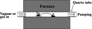
The vapour transport growth took place in a 1.5-inch-diameter quartz tube laid down in a rapid thermal furnace. shows the schematic illustration of the vapour transport system. The Zn particles (indicated as Zn) and the substrate (labelled as S) were located at a distance of about 10 cm in the centre of the quartz tube. P-type Si(100) wafers with diameter of 2.5 cm after cleaned by acetone and alcohol were used as substrates. The Au-covered Si substrates were prepared by depositing a 200 nm thick layer of Au film on the cleaned Si(100) wafers using radio frequency sputtering (JC500-3/D) from an Au target.
Figure 1. Schematic illustration of the vapour growth system. The Zn particles source (Zn) and Si substrates (S) are located at a distance of 10 cm.
The synthesis procedure included the following steps: (1) flowing Ar gas through the quartz tube for 0.5 h to remove the air in it; (2) increase the furnace temperature to 800°C with the Ar gas flow; (3) maintain the temperature at 800°C for 1 h and replace the Ar flow by a mixture of either Ar/H2O vapour or Ar/O2 gas. The pressure of the quartz tube is maintained at 0.03∼0.05 MPa; (4) switch off the furnace and cool down the sample to RT at the rate of 7°C per minute. The reactions of metallic Zn with H2O vapour and O2 gas can be written, respectively, as following:
(1)
(2) One may note that when H2O is used as oxidant, H2 gas is produced in the quartz tube.
The morphologies of the samples were characterised by SEM (LEO-1530FE-SEM). The crystal structures were analysed by XRD within the 2θ range of 30°–65° at a scan rate of 0.0167°/step, using PANalytical X'pert PRO X-ray diffractometer with Cu-Kα radiation source. PL measurements were taken at RT using a KrF excimer laser line of 248 nm as the excitation source with a Hitachi F4500 PL spectrophotometer.
3. Results and discussion
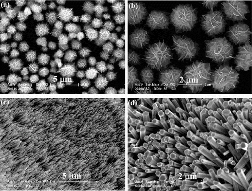
The morphologies of the ZnO nanostructures prepared in H2O vapour and O2 gas are shown in . ZnO nanoflowers were synthesised in H2O vapour as indicated in (a) and 2(b). The nanoflowers are constructed by tens of ZnO nanosheets with random orientations. However, ZnO hexagonal nanorods arrays were formed in the O2 gas as shown in (c) and 2(d). The size of the nanorods is not uniform which may be influenced by the size of the Au catalyst underneath.
Figure 2. SEM images of the ZnO nanostructures grown in: (a) and (b) H2O vapour; (c) and (d) O2 gas.
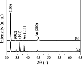
The influence of the atmosphere on the ZnO crystal structure is depicted in . Both samples show hexagonal wurtzite structure. The diffraction peaks appear at 31.78°, 34.34° and 36.23°, which correspond to (100), (002) and (101) planes in the ZnO wurtzite structure (JCPDS 36-1451), respectively. Except for the diffraction peaks from Au, no other detectable peaks from impurity phases such as Zn or Zn(OH)2 are observed. The sample synthesised in O2 gas shows a preferential ⟨001⟩ orientated structure with the dominant (100) diffraction peak, which is consistent with the result derived from the SEM images. The nanorods, as shown in (c) and 2(d), display a ⟨001⟩ orientation vertical to the substrate. The sample synthesised in H2O vapour does not show a preferential orientation – for example, some intense peaks corresponding to (002) and (101) phases are also found.
Figure 3. XRD patterns of the ZnO nanostructures grown in: (a) H2O vapour; (b) O2 gas.
ZnO crystal grows preferentially along the ⟨001⟩ direction due to the lowest surface energy of the (002) facet. Therefore, ZnO nanowires or nanorods are often obtained. But ZnO is eroded in H2 gas and the final dimension of the nanostructure is thus determined by a competition between crystal growth and etching. ZnO nanosheets can be grown by suppressing the growth along the ⟨001⟩ direction.[Citation14] Tian et al. [Citation15] demonstrated that citrate ions could slow down the crystal growth rate along the ⟨001⟩ orientation and consequently plate-like ZnO rather than rod-shaped would be produced in solutions with high citrate ions concentration. For crystal growth, after initial nucleation, the subsequent growth stage strongly governs the final morphology of the crystal. In the O2 gas, the growth of ZnO is simply along the ⟨001⟩ direction due to the fastest growth kinetics in this direction and absence of side or reverse reactions. However, in the H2O vapour the growth of ZnO crystal is not as easy as in O2 gas, because the enthalpy of the reaction (ΔrH) for reaction (1) is larger than that for reaction (2). Also, the formation of H2 in reaction (1) would be generally inhibited, especially in c-direction, by removal of the O species in the ZnO crystal, as indicated in the following equation:
(3)
The reaction (3) reduces the ZnO growth rate and subsequently makes it possible to create more nuclei seeds simultaneously at different orientations. This results in a more complicated growth mechanism and induces the formation of ZnO nanoflowers as shown in (a) and 2(b).
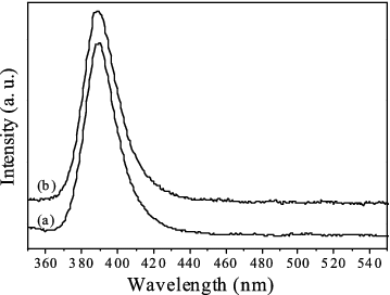
The optical properties of the synthesised ZnO samples were investigated by PL spectroscopy (see in ). It is interesting to find that both the PL spectra consist of only a strong UV peak attributed to the near-band-edge excitonic transition of ZnO [Citation16] at 389 nm (3.18 eV). The full width at half-maximum (FWHM) of the peaks are calculated to be 0.19 and 0.15 eV for spectra (a) and (b), respectively. The wider FWHM for the ZnO nanostructure grown in H2O vapour may result from the possible H impurities in the ZnO lattice.[Citation17] There is no green emission peak, which is related to some deep levels induced by defects, e.g. oxygen/Zn vacancies/interstitials [Citation18] or impurity levels in the spectra. It is well known that PL spectrum depends on the stoichiometry of ZnO nanostructures.[Citation19] Thus, this result indicates that the synthesised ZnO nanostructures are with good chemical composition and of optically high quality.
Figure 4. Room-temperature PL spectra of the ZnO nanostructures synthesised in: (a) H2O vapour; (b) O2 gas.
4. Conclusions
ZnO nanostructures have been synthesised by reaction of Zn vapour with H2O vapour and O2 gas using a vapour transport technique. SEM and XRD studies indicated that the growth orientation of ZnO strongly depends on the use of oxidant species. Though the samples showed different morphologies and crystal structures, surprisingly, they had almost same optical properties. The PL spectra revealed only one UV peak at near 389 nm in wavelength for both samples, indicating the high quality of the synthesised ZnO samples. The results presented in here also indicated that different nanostructures of ZnO could be manipulated simply in different atmosphere with the vapour transport method.
Acknowledgements
The author would like to thank Quanzhou Normal University and Quanzhou ‘Tong-Jiang Scholar’ programme for financial support.
References
- Huang MH, Mao S, Feick H, Yan H, Wu Y, Kind H, Weber E, Russo R, Yang PD. Room-temperature ultraviolet nanowire nanolasers. Science. 2001;292:1897–1899.
- Morgan JH, Brodie DE. The preparation and some properties of transparent conducting ZnO for use in solar cell. Can J Phys. 1982;60(10):1387–1390.
- Vanheusden K, Seager CH, Warren WL, Tallant DR, Voigt JA. Correlation between photoluminescence and oxygen vacancies in ZnO phosphors. Appl Phys Lett. 1996;68(3):403–405.
- Size SM. Semiconductor sensors. New York (NY): J. Wiley; 1994.
- Zheng ZY, Chen TX, Cao L, Han YY, Xu FQ. Structure and optical properties of ZnO nanowire arrays grown by plasma-assisted molecular beam epitaxy. J Inorg Mater. 2012;27(3):301–304.
- Chang P-C, Fan Z, Wang D, Tseng W-Y, Chiou W-A, Hong J, Lu JG. ZnO nanowires synthesized by vapor trapping CVD method. Chem Mater. 2004;16(24):5133–5137.
- Jain S, Kodas TT, Hampden-Smith M. Synthesis of ZnO thin films by metal-organic CVD of Zn(CH3COO)2. Chem Vapor Depos. 1998;4(2):51–59.
- Li ZY, Xu FC, Wu Q-H, Li J. Zinc oxide thin film synthesized by combustion chemical vapor deposition. Appl Surf Sci. 2008;255(5):2859–2863.
- Li G. Synthesis of aligned ZnO nanocolumn arrays by a vapor phase transport method. Russ J Phys Chem A. 2012;86(13):1991–1994.
- He GN, Wu ST, Li J, Huang B, Wu QH. Influence of pH value on the structures and optical properties of ZnO nanocrystalline synthesized with a solution process. Funct Mater Lett. 2010;3(2):107–110.
- He GN, Huang B, Wu ST, Li J, Wu QH. Structure morphologies and luminescence properties of ZnO nanomaterials synthesized by an acidic solution process. J Phys D: Appl Phys. 2009;42(21):215401.
- Orhan N, Baykul MC. Characterization of size-controlled ZnO nanorods produced by electrochemical deposition technique. Solid-State Electron. 2012;78:147–150.
- Chantarat N, Chen YW, Li CC, Chiang MC, Chen YC, Chen SY. Nitrogen plasma-assisted codoped p-type (In, N):SnO2 ultra-fine thin films and N-ZnO/p-In:SnO2 core-shell heterojunction diodes fabricated by an ultrasonic spray pyrolysis method. J Phys Chem C. 2011;115(46):23113–23119.
- Ghosh R, Basak D, Fujihara S. Effect of substrate-induced strain on the structural, electrical, and optical properties of polycrystalline ZnO thin films. J Appl Phys. 2004;96(5):2689–2692.
- Tian ZR, Voigt JA, Liu J, Mckenzie B, Mcdermott MJ, Rodriguez MA, Konishi H, Xu H. Complex and oriented ZnO nanostructures. Nat Mater. 2003;2:821–826.
- Zhang Y, Jia HB, Yu DP, Wang RM, Luo XH. Low-temperature growth and Raman scattering study of vertically aligned ZnO nanowires on Si substrate. Appl Phys Lett. 2003;83(22):4631–4633.
- Bjorheim TS, Erdal S, Johansen KM, Knutsen KE, Norby T. H and Li related defects in ZnO and their effect on electrical properties. J Phys Chem C. 2012;116(44):23764–23772.
- Vanheusden K, Warren WL, Seager CH, Tallant DK, Voigt JA, Gnade BE. Mechanisms behind green photoluminescence in ZnO phosphor powders. J Appl Phys. 1996;79:7983–7890.
- Zu P, Tang ZK, Wong GK, Kawasaki LM, Ohotomo A, Koinuma H, Segawa Y. Ultraviolet spontaneous and stimulated emissions from ZnO microcrystallite thin films at room temperature. Solid State Commun. 1997;103(8):459–463.