
Abstract
In this work, we display one-step reactions under autogenic pressure at elevated temperature (RAPET) method-based synthesis of Mn-doped GaN nanorods by varying the atomic ratio of Mn:Ga as 0, 0.02, 0.04, 0.06 and 0.08, respectively. The synthesised nanorods are characterised by X-ray diffraction, high-resolution transmission electron microscopy (HRTEM) and Raman spectral methods. It is observed that there is a decrease in the lattice constant with an increase in the concentration of Mn (from 0.02 to 0.08 wt%). Moreover, the smaller covalent radius of Mn is the key for the doping process. The Mn-doped GaN nanocrystals show rod-like morphology with a length of 40–50 nm and width of 8–12 nm. This size factor mainly depends on the doping of Mn [from transmission electron microscopy (TEM) analysis] into GaN components. Well-defined lattice fringes are elucidated for the growth of crystalline hexagonal GaN (wurtzite type) nanocrystals.
1. Introduction
Smart nanomaterials have received enormous attention in recent times due to their application in novel nanoelectronic and optoelectronic devices.[Citation1–8] It has been used in many functional devices owing to their unique one-dimensional nanostructures, excellent electronic and optical properties.[Citation1–8] More specially, wide-band gap semiconductors (III Group-N) such as AlN, GaN (3.4 eV) and InN have attracted extensive attention as they exhibit very high optical efficiencies. Of course, the above-mentioned nanomaterials have been successfully used in many electronic devices such as high-power and high-frequency transistors, blue and ultraviolet light-emitting diodes and laser diodes. Very recently, it is used as the most promising nanomaterial for spintronic device application. This is because of the fact that the dilute magnetic semiconductors (DMS) based on these materials showed the stability of the ferromagnetism at temperatures higher than the room temperature.[Citation9–14] GaN is an excellent host material to be successfully made into DMS according to the computed value at high Curie temperature (TC).[Citation9] This interesting property created immense interest in the research community. The interest was because of their possible applications for the design of spintronic nanodevices,[Citation15,16] such as electronic-optic switches, ultrasensitive magnetic field sensors, magnetic hard disk media, spin field effect transistors, resonant tunnelling diodes and non-volatile computer memory chips.[Citation17–19] After the discovery of ferromagnetism with a higher temperature in Mn-doped GaN,[Citation9,Citation20] there has been a remarkable interest towards the fabrication of GaN-based DMS. Hence, the research community is extremely interested to prepare DMS. The primary goal of such fabrication of Mn-doped GaN is realising room temperature ferromagnetism and therefore posing it as a potential candidate for future spintronics applications.[Citation21]
The GaN materials have been extensively studied and predicted to be ferromagnetic with a TC above room temperature. However, many reported experimental values were quite different and even contradictory. Near or above room temperature, ferromagnetism was found by a number of groups,[Citation20,Citation22–29] whereas no ferromagnetism or a very low TC was reported.[Citation30,31] A number of approaches have been explored to synthesise single-phase Mn-doped GaN, which includes epitaxial growth, chemical vapour deposition, pulse laser deposition, sputtering,[Citation32–35] solvothermal,[Citation36,37] azidothermal metathesis,[Citation38] sublimation sandwich method [Citation39] and carbothermal nitridation.[Citation40] In this work, we demonstrate a simple, efficient and economical synthesis method for the fabrication of nanocrystalline Mn-doped GaN nanorods. The Mn-doped GaN nanorods are obtained in a crystallised form through a single-stage, solvent-free and catalyst-free single precursor reaction. In addition, the reaction is conducted at a relatively lower temperature, i.e. 750 °C, as compared to other methods for the formation of GaN nanocrystals and we named such reaction as reactions under autogenic pressure at elevated temperature (RAPET). Indeed, a survey of the experimental literature reveals that the carbon encapsulated NiO/MgO core/shell structured [Citation41] and Mn-doped CdSe [Citation42] nanostructured materials have been synthesised and reported by the RAPET method.
2. Experimental
Gallium(III) chloride, anhydrous beads – 10 mesh (GaCl3, Aldrich, 99.99%), manganese(II) chloride, anhydrous beads – 10 mesh (MnCl2, Aldrich, 99.99%) and sodium azide (NaN3, Aldrich, 99.99%) were received from Sigma Ltd and were used as the starting precursor materials. In a typical synthesis of Mn-doped GaN nanocrystals, 0.501 g of GaCl3, 0.061 g of NaN3 and stoichiometric amount of anhydrous MnCl2 (according to Mn/Ga atomic ratios of 0, 0.02, 0.04, 0.06 and 0.08) were mixed and introduced into a 2 ml stainless steel Swagelok reactor at room temperature. It is placed inside the glove box under N2 atmosphere. The filled Swagelok reactor is tightly closed with the other plug and placed at the middle of furnace tube. The temperature of the furnace is raised to 750 °C at a rate of 10 °C min−1 and maintained in this temperature for 7 hr. The Swagelok reactor is gradually cooled (∼5 hr) to room temperature and opened. The yield of the yellowish-green coloured Ga1−xMnxN product is ∼52%. The Ga1−xMnxN products with Mn/Ga atomic ratios of 0, 0.00, 0.04, 0.06 and 0.08 are determined by inductively coupled plasma (ICP) analysis.
A morphological characterisation of the obtained nanocrystals was done by using high-resolution transmission electron microscopy (HRTEM, JEOL JEM, 2010) with an acceleration voltage of 200 kV measurements. Sample for high-resolution transmission electron microscopy (HRTEM) analysis were prepared by ultrasonically dispersing the product into absolute ethanol followed by placing a 3 μL of nanocrystals suspension onto a copper grid coated with an amorphous carbon film supported and then dried in vacuum. X-ray diffraction (XRD) patterns were obtained on a Bruker AXS D8 diffractometer using CuKα 1.5418 Å radiation at step scan 0.02θ, from 20 to 80θ and energy dispersive X-ray spectroscopy (EDS, JEOL, 2010). Raman spectral measurements were performed by using Olympus BX41 (Jobin-Yvon-Horiba) spectrometer with the wavelength source of 514.5 nm line of an Ar ion laser.
3. Results and discussion
3.1. XRD and elemental analysis (ICP)
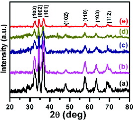
The XRD patterns of the nanocrystalline Ga1−xMnxN (x = 0.00, 0.02, 0.04, 0.06, 0.08) products were shown in (a)–(e). Sharp and well-defined peaks were observed for the earlier mentioned samples at 2θ values of 32.4°, 34.7°, 36.9°, 48.2°, 57.9°, 63.6°, 68.1°, 70.2° and 71.3° corresponding to (100), (002), (101), (102), (110), (103), (200), (112) and (201) nanocrystalline planes. All these peaks could be indexed to a hexagonal GaN phase with lattice constant values of a = 0.3186 nm and c = 0.5178 nm. The obtained lattice constant values matched well with the values of GaN. The calculated lattice constant values of the Mn-doped GaN nanocrystaline powders, with different Mn concentrations are listed in . It can be seen that the lattice constants, ‘a’ and ‘c’ shrink upon Mn doping and this suggests that the substitution of Mn into the GaN lattice. The shrinkage of both ‘a’ and ‘c’ is due to the covalent radius of Mn (1.17 Å) is smaller than that of Ga (1.26 Å). Furthermore, no diffraction peaks of Ga2O3 or other impurities were found in our samples. This result indicates that the as-prepared samples were of highly nanocrystallinity. The average crystallite size was calculated for pure GaN nanocrystals using the Debye–Scherrer formula (i) for the prominent plane of (101).(1)
Table 1. Lattice constant parameters of Mn-doped GaN nanorods versus various atomic compositions.
Figure 1. XRD patterns of Ga1−xMnxN nanorods. (a) x = 0.0, (b) x = 0.02, (c) x = 0.04, (d) x = 0.06 and (e) x = 0.08, respectively.
3.2. HRTEM analysis
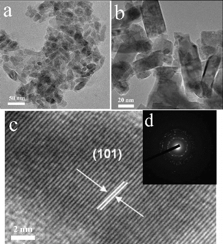
The HRTEM was used to investigate the shape and size of the nanocrystals by varying the Mn/Ga atomic ratio. Selected area energy dispersive elemental analysis was also used for the identification of the product GaN and crystalline behaviour. The HRTEM images of undoped nanocrystalline GaN nanocrystals were shown in , which clearly indicate that the nanocrystals were polydispersed and not uniform. As shown in (b), the morphology is capsule-like shape and the dimensions were of 10–20 nm length and 3–5 nm width, respectively. Interestingly, a gradual increase in the nanocrystal size was observed when the concentration of Mn was increasing. The clear nanorods morphology of GaN nanocrystals were observed at the higher concentration of Mn. The TEM images of nanocrystalline GaN shown in (a) and (b). The Mn-doped GaN nanocrystals showed the rod-shaped morphology and the size range of 40–50 nm of length and 8–12 nm of width. As shown in (c), the HRTEM illustrates the well-defined lattice fringes, indicating that the higher nanocrystalline nature of the Mn-doped GaN nanorods. The measured inter-planar d-spacing value of (101) lattice plane is 2.45 Å. The above values were in good agreement with the reported value of d101 = 2.43 Å [Joint Committee on Powder Diffraction Standards (JCPDS), No. 074–0243]. The selected area electron diffraction (SAED) pattern showed the formation of pre-dominant GaN (100), (002) and (101) ring patterns indicating the nanocrystalline behaviour of the GaN nanorods ((d)).
Figure 2. HRTEM images of undoped GaN nanocrystals.
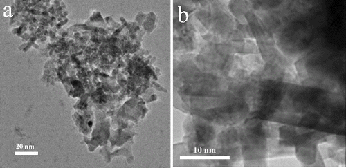
Figure 3. HRTEM images of Mn-doped (x = 0.08) GaN nanorods (a–c) and the corresponding SAED pattern of Mn-doped GaN nanorods (d).
3.3. Raman spectroscopy
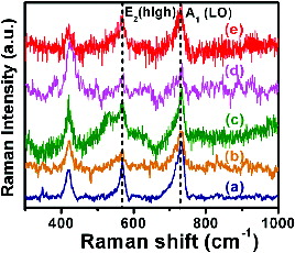
The Raman spectral features of Mn-doped GaN nanorods were shown in . The Raman peaks were observed at 420, 560 and 740 cm−1. The Raman spectrum of GaN nanorods showed strong E2 (high) and A1 (LO) modes at 560 and 740 cm−1.[Citation43] These modes were in good agreement with Raman selection rules for wurtzite type of GaN nanorods. The high intensity of A1 (LO) mode in undoped GaN nanorods indicates the low concentration of free carriers in the material. Moreover, a comparison of A1 (LO) modes in the spectrum of Mn-doped GaN nanorods reveals an increase in the concentration of Mn from 0.02 to 0.08 as shown in (b)–(e). The A1 (LO) mode was decreased due to the doping of Mn into the GaN nanocrystals and a slight shift from 733 to about 720 cm−1 was observed. In addition, the E2H mode was also decreased, broadened but not shifted (at 567 cm−1). The shift of A1(LO) mode was due to the difference in bonding strengths between GaN and MnN compositions in Mn-doped GaN nanorods.[Citation44] The additional peak at ∼420 cm−1 was very close to the overtone processes of the acoustic phonons that are observed in a single crystal of GaN nanorods.[Citation45] The observed results clearly confirmed the successful doping of Mn into GaN nanorods. The synthesised Mn-doped GaN nanorods will be employed in the fabrication of nanoscale magnetic and optical devices. Currently these studies are under way in our laboratory.
Figure 4. Raman spectra of Ga1−xMnxN nanorods. (a) x = 0.00, (b) x = 0.02, (c) x = 0.04, (d) x = 0.06 and (e) x = 0.08, respectively.
4. Conclusions
We have demonstrated the RAPET method-based synthesis of Mn-doped GaN nanorods by varying the ratio of Mn:Ga (0, 0.02, 0.04, 0.06 and 0.08) components. Nanocrystalline phase of the GaN nanorods were confirmed by XRD measurements and the relative intensity of the XRD peaks varied by increasing the concentration of Mn. Well-defined Mn-doped GaN nanorods and lattice fringes were illustrated in HRTEM images. This indicates the highly crystalline nature of Mn-doped GaN nanorods. The structural evidence for the formation of pure GaN nanorods was also confirmed from Raman spectral measurements. These well-defined and composition-tuneable Mn-doped GaN nanostructures would be able to provide new building blocks for various optical and magnetic devices.
References
- Cui Y, Wei Q, Park H, Lieber CM. Nanowire nanosensors for highly sensitive and selective detection of biological and chemical species. Science. 2001;293:1289–1292.
- Huang MH, Mao S, Feick H, Yan H, Wu Y, Kind H, Weber E, Russo R, Yang P. Room-temperature ultraviolet nanowire nanolasers. Science. 2001;292(5523):1897–1899.
- Kong XY, Ding Y, Yang R, Wang ZL. Single-crystal nanorings formed by epitaxial self-coiling of polar nanobelts. Science. 2004;303(5662):1348–1351.
- Ui S-W, Choi I-S, Choi S-C. Optical properties of one-dimensional structured GaN:Mn fabricated by a chemical vapor deposition method. J Eng. 2013;2013:216259–216264.
- Baliga BJ. Gallium nitride devices for power electronic applications. Semiconductor Sci Technol. 2013;28:074011–074018.
- Boukortt A, Hayn R, Virot F. Optical properties of Mn-doped GaN. Phys Rev B. 2012;85(3):033302–033305.
- Kibria MG, Nguyen HPT, Cui K, Zhao S, Liu D, Guo H, Trudeau ML, Paradis S, Hakima A-R, Mi Z. One-step overall water splitting under visible light using multiband InGaN/GaN nanowire heterostructures. ACS Nano. 2013;7(9):7886–7893.
- Gonzalez Szwacki N, Majewski JA, Dietl T. Aggregation and magnetism of Cr, Mn, and Fe cations in GaN. Phys Rev B. 2011;83(18):184417–184423.
- Dietl T, Ohno H, Matsukura F, Cibert J, Ferrand D. Zener model description of ferromagnetism in zinc-blende magnetic semiconductors. Science. 2000;287(5455):1019–1022.
- Sato K, Dederichs PH, Araki K, Katayama-Yoshida H. Ab initio materials design and Curie temperature of GaN-based ferromagnetic semiconductors. Physica Status Solidi (c). 2003;0(7):2855–2859.
- Hashimoto M, Zhou Y-K, Kanamura M, Asahi H. High temperature (Zn1−xMnxO) ferromagnetism in III–V-based diluted magnetic semiconductor GaCrN grown by ECR molecular-beam epitaxy. Solid State Commun. 2002;122(1–2):37–39.
- Wu SY, Liu HX, Gu L, Singh RK, Budd L, van Schilfgaarde M, McCartney MR, Smith DJ, Newman N. Synthesis, characterization, and modeling of high quality ferromagnetic Cr-doped AlN thin films. Appl Phys Lett. 2003;82(18):3047–3049.
- Sheu J-K, Huang F-W, Liu Y-H, Chen PC, Yeh Y-H, Lee M-L, Lai W-C. Photoresponses of manganese-doped gallium nitride grown by metalorganic vapor-phase epitaxy. Appl Phys Lett. 2013;102(7):071107–071109.
- Choi E-A, Kang J, Chang KJ. Energetics of cubic and hexagonal phases in Mn-doped GaN: first-principles pseudopotential calculations. Phys Rev B. 2006;74(24):245218–245224.
- Datta S, Das B. Electronic analog of the electro-optic modulator. Appl Phys Lett. 1990;56(7):665–667.
- Hegde M, Farvid SS, Hosein ID, Radovanovic PV. Tuning manganese dopant spin interactions in single GaN nanowires at room temperature. ACS Nano. 2011;5(8):6365–6373.
- DiVincenzo DP. Quantum computation. Science. 1995;270(5234):255–261.
- Prinz GA. Magnetoelectronics. Science. 1998;282(5394):1660–1663.
- Awschalom DD, Kawakami RK. Magnetoelectronics: teaching magnets new tricks. Nature. 2000;408:923–924.
- Reed ML, El-Masry NA, Stadelmaier HH, Ritums MK, Reed MJ, Parker CA, Roberts JC, Bedair SM. Room temperature ferromagnetic properties of (Ga, Mn)N. Appl Phys Lett. 2001;79(21):3473–3475.
- Wolf SA, Awschalom DD, Buhrman RA, Daughton JM, von Molnár S, Roukes ML, Chtchelkanova AY, Treger DM. Spintronics: a spin-based electronics vision for the future. Science. 2001;294(5546):1488–1495.
- Wang J, Chen P, Li Z, Guo X, Makino H, Yao T, Chen H, Huang Q, Zhou J, Lu W. Preparation and characterization of room-temperature ferromagnetism GaMnN based on ion implantation. Sci China Ser G: Phys Mech Astron. 2003;46(5):474–480.
- Theodoropoulou N, Hebard AF, Overberg ME, Abernathy CR, Pearton SJ, Chu SNG, Wilson RG. Magnetic and structural properties of Mn-implanted GaN. Appl Phys Lett. 2001;78(22):3475–3477.
- Sasaki T, Sonoda S, Yamamoto Y, Suga K-i, Shimizu S, Kindo K, Hori H. Magnetic and transport characteristics on high Curie temperature ferromagnet of Mn-doped GaN. J Appl Phys. 2002;91(10):7911–7913.
- Sardar K, Raju AR, Bansal B, Venkataraman V, Rao CNR. Magnetic, optical and transport properties of GaMnN films. Solid State Commun. 2003;125(1):55–57.
- Lee JM, Lee KI, Chang JY, Ham MH, Huh KS, Myoung JM, Hwang WJ, Shin MW, Han SH, Kim HJ, Lee WY. Ferromagnetic ordering of n-type (Ga,Mn)N epitaxial films. Microelectronic Eng. 2003;69(2–4):283–287.
- Yoon IT, Park CS, Kim HJ, Kim YG, Kang TW, Jeong MC, Ham MH, Myoung JM. Characterization of ferromagnetic Ga1−xMnxN layers grown on sapphire (0001) substrates. J Appl Phys. 2004;95(2):591–596.
- Zhang F, Chen N, Liu X, Liu Z, Yang S, Chai C. The magnetic and structure properties of room-temperature ferromagnetic semiconductor (Ga,Mn)N. J Crystal Growth. 2004;262(1–4):287–289.
- Ren H, Jian J, Chen C, Pan D, Ablat A, Sun Y, Li J, Wu R. Ga-vacancy-induced room-temperature ferromagnetic and adjusted-band-gap behaviors in GaN nanoparticles. Appl Phys A. 2013;113:1–7.
- Zajc M, Doradziński R, Gosk J, Szczytko J, Lefeld-Sosnowska M, Kamińska M, Twardowski A, Palczewska M, Grzanka E, Gȩbicki W. Magnetic and optical properties of GaMnN magnetic semiconductor. Appl Phys Lett. 2001;78(9):1276–1278.
- Overberg ME, Abernathy CR, Pearton SJ, Theodoropoulou NA, McCarthy KT, Hebard AF. Indication of ferromagnetism in molecular-beam-epitaxy-derived N-type GaMnN. Appl Phys Lett. 2001;79(9):1312–1314.
- Radovanovic PV, Barrelet CJ, Gradečak S, Qian F, Lieber CM. General synthesis of manganese-doped II–VI and III–V semiconductor nanowires. Nano Lett. 2005;5(7):1407–1411.
- Xu C, Chun J, Lee HJ, Jeong YH, Han S-E, Kim J-J, Kim DE. Ferromagnetic and electrical characteristics of in situ manganese-doped GaN nanowires. J Phys Chem C. 2006;111(3):1180–1185.
- Ham M-H, Oh D-K, Myoung J-M. Transport properties in (Ga,Mn)N nanowire field-effect transistors. J Phys Chem C. 2007;111(30):11480–11483.
- Ivanov YM. The growth of single crystals by the self-seeding technique. J Crystal Growth. 1998;194(3–4):309–316.
- Biswas K, Sardar K, Rao CNR. Ferromagnetism in Mn-doped GaN nanocrystals prepared solvothermally at low temperatures. Appl Phys Lett. 2006;89(13):132503–132505.
- Das SN, Patra S, Kar JP, Lee M-J, Hwang SH, Lee TI, Myoung J-M. Growth and characterization of Mg-doped GaN nanowire synthesized by the thermal evaporation method. Mater Lett. 2013;106:352–355.
- Wang J, Grocholl L, Gillan EG. Facile azidothermal metathesis route to gallium nitride nanoparticles. Nano Lett. 2002;2(8):899–902.
- Li PG, Lei M, Yang H, Tang HL, Guo YF, Tang WH. Magnetic and electrical transport properties of nanostructured La0.67Ca0.33MnO3 networks. J Alloys Compounds. 2008;460(1–2):60–63.
- Wang Z, Huang B, Yu L, Dai Y, Wang P, Qin X, Zhang X, Wei J, Zhan J, Jing X, Liu H, Whangbo M-H. Enhanced ferromagnetism and tunable saturation magnetization of Mn/C-codoped gan nanostructures synthesized by carbothermal nitridation. J Am Chem Soc. 2008;130(48):16366–16373.
- Mahendiran C, Maiyalagan T, Scott K, Gedanken A. Synthesis of a carbon-coated NiO/MgO core/shell nanocomposite as a Pd electro-catalyst support for ethanol oxidation. Mater Chem Phys. 2011;128(3):341–347.
- Bhattacharyya S, Zitoun D, Gedanken A. One-pot synthesis and characterization of Mn2+-doped wurtzite CdSe nanocrystals encapsulated with carbon. J Phys Chem C. 2008;112(20):7624–7630.
- Vajpeyi AP, Georgakilas A, Tsiakatouras G, Tsagaraki K, Androulidaki M, Chua SJ, Tripathy S. Effect of substrate temperature on spontaneous GaN nanowire growth and optoelectronic properties. Physica E: Low-dimensional Syst Nanostructures. 2009;41(3):427–430.
- Cui X-G, Zhang R, Tao Z-K, Li X, Xiu X-Q, Xie Z-L, You-Dou Z. Optical and structural properties of Mn-doped GaN grown by metal organic chemical vapour deposition. Chin Phys Lett. 2009;26:038103–038106.
- Wang ZL. Metal and semiconductor nanowires, XIII. Nanowires and Nanobelts: Mater Properties Devices. Vol. 1, 2003, p. 343–385.