
 ?Mathematical formulae have been encoded as MathML and are displayed in this HTML version using MathJax in order to improve their display. Uncheck the box to turn MathJax off. This feature requires Javascript. Click on a formula to zoom.
Abstract
In this work, different microfluidic colour-changing devices are implemented by using dry film photoresist-based moulds instead of standard photolithography moulds. EtertecHT-115T negative dry film photoresist is employed to realise the rapid fabrication of the moulds for colour-changing layers. The major factors that may affect the fidelity of the dry film moulds during fabrication are summarised and analysed, including the optimum exposure times and the appropriate developing times. Especially, the impacts of different concentrations of sodium carbonate (Na2CO3) solution on developing rate are investigated for 1–5 layers (50–250 μm thick) of EtertecHT-115T dry film photoresists by experiments. The created dry film moulds show the advantages of low cost, high manufacturing efficiency and requiring no professional training. Each application of the microfluidic colour-changing devices presents high transparency and good colour-changing effect. The microfluidic colour-changing layers based on dry film moulds can be used in different wearable devices of human, and also can be applied for realising surface camouflage and display functions of soft machines/robotics.
1. Introduction
Microfluidics is a rapidly expanding field with applications in a number of different markets including biochemical analysis [Citation1,Citation2], drug delivery [Citation3] and medical diagnose [Citation4,Citation5], due to the small sizes, high throughput and low cost of microfluidic systems [Citation6]. In recent years, some studies on the colour-changing function of microfluidic systems are reported. Morin et al. reported a microfluidic network to provide both camouflage/display and movement of a soft machine [Citation7]. In our previous reports, we proposed a microfluidic liquid colour-changing method, which was applied in different optical devices. By circulating colour liquids in microfluidic channels on the colour-changing layers, these devices can realise vision protection [Citation8], surface camouflage and optical filtering [Citation9]. However, the key step to fabricate these microfluidic devices is to make colour-changing layers with different channel structures by using microfluidic moulds, which need complex creating process and require large investments (including clean environment, well trained people, expensive photolithography equipments, etc.), and therefore become the development bottleneck for microfluidic research and application.
Dry film photoresist offers many advantages such as low cost, good uniformity of photoresist distribution, low exposure energy and near vertical sidewalls [Citation10]. It has been most commonly used in the patterning of printed circuit boards (PCBs) [Citation11] and electroplate moulds in Lithographie, Galvanoformung, and Abformung (LIGA)-type process [Citation12]. Recently, dry film photoresist also arises greater interests of the researchers in microfluidic field [Citation13,Citation14]. Smejkal et al. proposed a dry film photoresist microfluidic chip used for analysing the isotachophoresis of lactate in human serum [Citation15]. Horak et al. reported a disposable microfluidic immunochip, which employed photoresist film to biofunctionalize the channels to enhance electrochemical detection of a cardiac biomarker [Citation16]. Weltin et al. presented a flexible microsensor, which was fabricated on a wafer-level including a layer of dry film photoresist for insulation [Citation17]. Qu et al. provided an electrochemical micromachining technology of micro-dimple arrays on cylindrical inner surfaces using GPM200 dry film photoresist [Citation18]. Kling et al. developed a microfluidic platform enabling the electrochemical readout of up to eight enzymelinked assays (ELAs), dry film photoresist served as the channel material in this system because it allowed long storage of preimmobilized assays [Citation19]. However, the microstructures in these devices are directly defined and machined by using dry film photoresists, which are fine for most cases such as liquid/gas transferring and biochemical tests, but impossible for some optical applications, because optical transparency is not considered in these microfluidic systems.
Here, we develop the application of EtertecHT-115T dry film photoresist (50 μm thick) in the moulds implementation for different microfluidic colour-changing devices, including colour-changing glasses, camouflage glasses and colour-changing starfish. The key parameters in the moulds fabrication are analysed and optimised for 1–5 layers (50–250 μm thick) of dry film photoresists by experiments. Different sizes of microstructures for each application can be personal designed and rapidly realised by this low-priced way without need of professional training and expensive equipments. Two or multilayer structures of colour-changing devices can also be easily achieved for more complex functionality by using this method.
2. Experimental procedures
2.1. Experimental materials
In this paper, 10:1 mixture of sylgard 184 silicone elastomer and curing agent (Dow Corning Corporation, USA) is employed to fabricate the PDMS colour-changing layers. EtertecHT-115T (Eternal Chemical Industry Limited Company, China), a negative dry film photoresist with 50 μm thick, serve as the material of the moulds patterns. In order to improve the flatness and accuracy of the moulds, 10 cm ×10 cm ×2.5 cm mirror stainless steel plates (Xingyang Stainless Steel Company, China) with very smooth surfaces are selected as the substrates of dry film moulds. 365 nm UV lamp (ShunyingPhoto Electricity Limited Company, China) is used for exposure. Anhydrous sodium carbonate, deionised water and nitrogen (Zhongjia Chemical Company, China) are used for developing, cleaning and drying during the experiments. In order to realise irreversible bonding, air plasma cleaner (Wenchang Chip Technology Limited Company, China) is prepared for surfaces treatment.
2.2. Fabrication of the microfluidic moulds by using EtertecHT-115T dry film photoresist
The fabrication process of the microfluidic moulds by using EtertecHT-115T negative dry film photoresist is shown in . The photomask is prepared by printing the designed micropatterns on a transparency film at 2400 dpi. Compared with conventional glass/metal material, the film photomask can not only meet resolution requirement, but also show the advantages of low-cost, fast and convenient for manufacturing, thus makes the dry film etch technology more accessible to an out-of-clean room environment.
Figure 1. The moulds fabrication for microfluidic colour-changing devices by using EtertecHT-115T dry film photoresist. (a) Peel off one of the translucent substrates from dry film photoresist. (b) Laminate the dry film photoresist (10 cm ×10 cm) on the cleaned mirror stainless steel substrate (10 cm ×10 cm ×2.5 cm) by using an office laminator at 110. (c) Overlap the three sheets (PMMA cover plate, prepared photomask sheet and mirror stainless steel substrate) as shown. (d) Fix around with clips to avoid light leaking. (e) Irradiate under 365 nm UV lamp at a distance of 15 cm. (f) Peel off the other translucent substrate from the dry film photoresist. (g) Immerse in 1% (mass concentration) Na2CO3 solution for developing. (h) Clean the developed structure with deionised water and dry it in nitrogen stream.
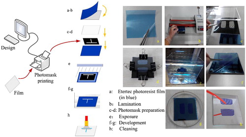
Then, transfer the designed microfluidic patterns from the photomask to the dry film photoresist sheet through the following process: Clean the mirror stainless steel plate with deionised water, dry it in nitrogen stream, and used as the substrate of the mould. Cut the dry film photoresist into 10 cm ×10 cm square. Peel off one of the translucent substrates pre-coated over the two surfaces of the photoresist (). Laminate the dry film photoresist (the surface with no translucent substrate should be faced down) on the cleaned mirror stainless steel substrate by using an office laminator at (). Place the printed photomask on the dry film photoresist and cover it with a transparent Polymethyl Methacrylate (PMMA) plate, fix some clips around the whole structure to avoid light leaking (). Expose the whole structure under an UV lamp with the power of 5 mW/cm2 for about 80 s (). Peel off the other translucent substrate pre-coated over the photoresist and immerse the structure into 1% (mass concentration) sodium carbonate (Na2CO3) developer solution at 25
for about 1 min (). The 80 s exposure time and 1 min developing time are only good for single-layer (50 um thick) dry film photoresist.
Finally, clean the developed structure with deionised water to wash away the unexposed portion and appear the engraved patterns as designed, then dry it in nitrogen stream (). It can be used as the microfluidic colour-changing mould now.
2.3. Fabrication of the microfluidic colour-changing devices using dry film moulds
In this paper, polymer PDMS is selected to make the colour-changing layer of the microfluidic devices due to its characters [Citation20,Citation21], such as high optical transparency in clean environments, less fragile and less expensive. More importantly, it is very convenient to make microfluidic devices with PDMS by using dry film moulds. The fabrication of the microfluidic colour-changing devices is based on soft lithography technology [Citation22–24]. It mainly includes two processes:fabrication of the PDMS film with microstructures by using dry film mould and irreversible bonding with substrate [Citation25–27].
The fabrication process of the PDMS film by using dry film mould is depicted in . Appropriate (according to the thickness of PDMS film to be made) mixture of liquid PDMS and curing agent at 10:1 in weight is prepared. Pour the mixture over the dry film mould and degas in vacuum environment for 1 h. Then put the whole structure into a vacuum oven at 80 and cure it for 20 min. Peel off the partial cured PDMS film with microstructures from the dry film mould, and poke two holes at the inlet and outlet of the microfluidic patterns respectively with a 1 mm diameter puncher. One is used as liquid inlet and the other is air outlet.
Figure 2. Fabrication process of the microfluidic colour-changing devices by using dry film moulds. (a) Fabrication of the PDMS film with microstructures. (b) Irreversible bonding of PDMS film with substrate (glass, resin or plastic).
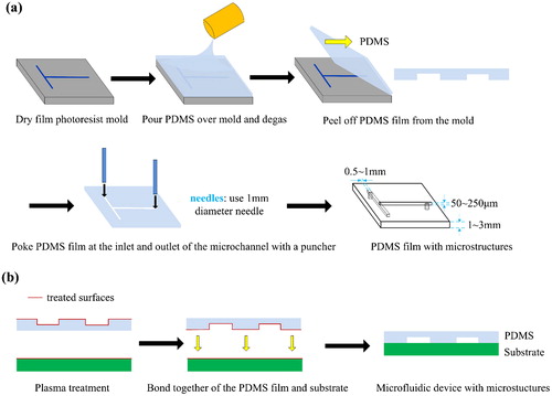
The fabricated PDMS film with microstructures is bonded on the substrate (glass, resin or plastic) to form closed microfluidic channels for colour liquids circulation. In order to achieve irreversible bonding (strong enough to withstand a high supply pressure), the two surfaces to be bonded are firstly modified by using air plasma cleaner at 80 W for 35 s, which can increase the number of surface oxide sites and improve their hydrophily [Citation28–30]. Then place the two treated surfaces together within 1 min and press gently so as to be a full contact. Finally, cure the bonding structure in a vacuum oven at 80 for 1 h to make sure of that the bonding strength is strong enough. The specific irreversible bonding process is described in .
3. Results and discussions
3.1. Fidelity of the microstructures on dry film moulds
The fidelity of the microstructures on dry film moulds can directly affect the performances of the microfluidic colour-changing devices after fabrication. The major factors that affect the fidelity of the dry film moulds are investigated, including bubble, exposure time, developing time, and developer concentration.
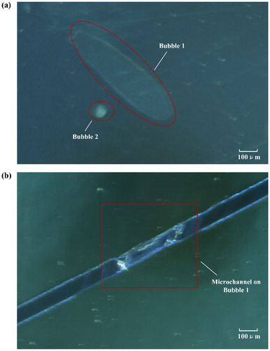
When laminating dry film photoresist on the substrate, bubbles will be easily formed between the photoresist and substrate, resulting in irregular channel boundaries. shows two formed bubbles between single-layer EtertecHT-115T dry film photoresist and mirror stainless steel substrate. One of the bubbles is located on the microfluidic channel exactly, thus irregular channel boundary is formed, as demonstrated in . So, bubble examination after lamination is very necessary. In this research, bubble examination is carried out through micro-observations by using light microscope XSP-63B (Shanghai Optical Instrument Company, China). If the measured bubble diameter is less than 1/5 of the minimum channel width, the bubble influence can be neglected. Otherwise, dry film lamination and bubble examination must be repeated.
Figure 3. The effect of bubble on dry film mold. (a) Two formed bubbles between EtertecHT-115T dry film photoresist and mirror stainless steel substrate after lamination. (b) The irregular channel boundary caused by bubble.
Among the factors that influence the moulds fidelity, exposure time is most crucial. presents the microscope images of the microfluidic channels with different photoresist thickness under overexposure, underexposure and appropriate exposure, respectively. It is obvious that overexposure makes the extra photoresist around the channels unwashable, resulting in wider channel structures than mask graphics, whereas underexposure makes the photoresist unable to be polymerised completely and easily to be washed off, resulting in obscurer and narrower channel structures than mask graphics. Through a large number of experiments, the general exposure time ranges for 1–5 layers (50 μm–250 μm thick) of EtertecHT-115T dry film photoresists are obtained. Another six measurements are conducted for each obtained time range, then the optimum exposure time ranges for different thickness dry film photoresists are summarised and proposed, as illustrated in .
Figure 4. Microscope images of the microfluidic channels under different exposure times for different dry film photoresist thickness. (a) 50 μm thick, (b) 100 μm thick, (c) 150 μm thick.
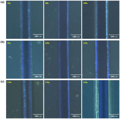
Figure 5. Experimental results of exposure times and developing times for 1–5 layers (50–250 μm thick) of EtertecHT-115T dry film photoresists. (a) The optimal exposure times, (b) The developing times by using different concentrations of developer solution.
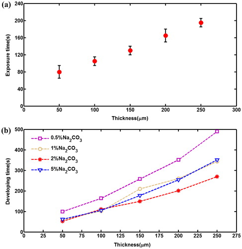
Developing process is also an important part in the mould fabrication with dry film photoresist. Underdevelopment leads to insufficient depths of channels, overdevelopment makes the dry film microstructures weak and easily to be destroyed. Commonly, 1% (mass concentration) Na2CO3 solution is used for development. In this paper, in order to investigate the influence of developer concentration on developing rate, different concentrations of Na2CO3 solutions are tested by experiments, as shown in .
indicates that the developing rate is not stable for the same concentration of developer solution, the longer the developing time lasts, the slower the developing rate becomes. The mainly reason is that the photoresist dissolved in the developer gradually increases as the growth of the developing time, resulting in the decreases of the developer effective concentration.
also provides the developing times for various dry film thickness by using different concentrations of Na2CO3 solutions. When the thickness is 100 μm, the developing time of 1% Na2CO3 is 102 s. For 0.5%, 2% and 5% Na2CO3, they are 184 s, 111 s and 105 s, respectively. And when the thickness is 250 μm, the developing time of 1% Na2CO3 is 344 s. For 0.5%, 2% and 5% Na2CO3, they are 490 s, 270 s and 351 s, respectively. Therefore, it is not that the higher the concentration is, the faster the developing rate becomes. The experimental results indicate that when the dry film thickness is less the 100 μm, 1% Na2CO3 solution has almost the same developing rate with 2% and 5% Na2CO3, this is the reason why it is widely used in the industry. However, when the thickness is greater than 100 μm, the developing rate of 2% Na2CO3 solution is obviously faster than 1% and 5% Na2CO3.
presents the time-consuming comparison by using different moulds making methods. Compared with conventional photolithography way, the moulds fabrication based on dry film photoresist shows high efficiency, and no expensive equipments and professionals are needed. However, the channels resolution is lower for dry film photoresist moulds, which are suitable for wider channels (>20 µm) prototyping or beginners in this field.
Table 1. Time-consuming comparison of using dry film photoresist and standard photolithography.
3.2. The applications of the colour-changing devices based on dry film photoresist moulds
presents the microfluidic colour-changing devices with different dimensions fabricated by using dry film photoresist moulds, including colour-changing glasses, camouflage glasses and colour-changing starfish. depicts the application effects, reveal the specific designs of the microstructures for each application. The microfluidic colour-changing glasses can be used to comfort and protect human eyes in an environment with strong lights by circulating colour liquids through the colour-changing layer. By designing disruptive microstructures on the lens and filling with proper colour liquids matched to the background environment, simple camouflage effect of the glasses can be achieved for concealing needs in the wilderness. Inspired by some coloured animals with special colour-changing organisms [Citation31] (such as chameleon), a colour-changing device similar to starfish is designed in this paper. With the simple liquid colour-changing layers matched to the environment around, the starfishes can camouflage and protect themselves from hunting. Each application presents good colour-changing effect and high transparency.
Figure 6. The applications of microfluidic colour-changing devices fabricated by dry film moulds. (a) The colour-changing effects of different microfluidic devices: (i) and (ii) colour-changing glasses, (iii) and (iv) camouflage glasses, (v)–(viii) colour-changing starfish. (b) Designs of the microstructures in . (c) Cross-sectional schematic of the regions indicated by the dotted yellow lines in .
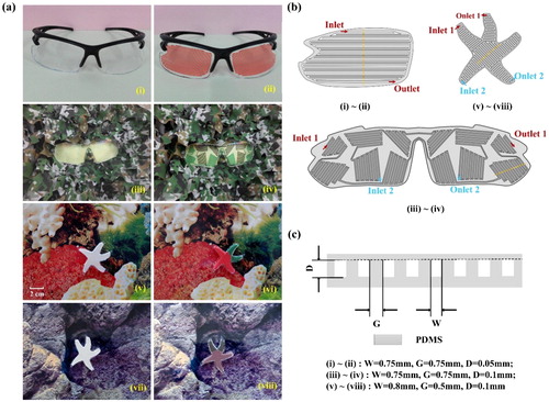
Other colour-changing and camouflage effects can be realised by changing the designs of microstructure on the dry film moulds. Two or multilayer structures of colour-changing devices can also be easily fabricated by this method to meet different requirements. Through targeted designing and making, the microfluidic colour-changing layers based on dry film moulds can be used in other various wearable devices for human. Meantime, they also can be applied for realising surface camouflage and display functions of soft machines/robotics, which have widespread usage in military.
4. Conclusions
From the fabrication and applications of the microfluidic colour-changing systems based on the dry film photoresists moulds, it can be concluded that the microfluidic moulds for different colour-changing devices can be rapidly realised by using EtertecHT-115T dry film photoresist and high-resolution masks. Proper selection of exposure times, developing time and concentration of developer solution for different dry film thickness can achieve good moulds performances. Different designs of the micropatterns and multilayer structures can be easily and quickly implemented by using dry film moulds. Each design and application of the microfluidic colour-changing device shows good colour-changing effect and high optical transparency. This fabrication and colour-changing ways also present new appearance modifying opportunities for other wearable devices of human and machines.
Acknowledgments
The authors would like to give their acknowledgement to the National Natural Science Foundation of China for the financial support (grant number 51175101).
Disclosure statement
The authors declared no competing financial interests.
Additional information
Notes on contributors
Songjing Li
S.L. conceived and designed the research. M.Z. and S.L. wrote the main manuscript text. M.Z did all the experiments and prepared all the figures. All the authors contributed to the discussion of the results and reviewed the manuscript.
References
- Shih SC, Gach PC, Sustarich J, et al. A droplet-to-digital (D2D) microfluidic device for single cell assays. Lab Chip. 2015;15:225–236.
- Liberale C, Cojoc G, Bragheri P, et al. Integrated microfluidic device for single-cell trapping and spectroscopy. Sci Rep. 2013;3:1–6.
- Majedi FS, Hasani-Sadrabadi MM, Emami SH, et al. Microfluidic assisted self-assembly of chitosan based nanoparticles as drug delivery agents. Lab Chip. 2013;13:204–207.
- Lee SH, Rhee HW, van Noort D, et al. Microfluidic bead-based sensing platform for monitoring kinase activity. Biosens Bioelectron. 2014;57:1–9.
- Ng Alphonsus HC, Uddayasankar Uvaraj, Wheeler Aaron R. Immunoassays in microfluidic systems. Anal Bioanal Chem. 2010;397:991–1007.
- Yager P, Edwards T, Fu E, et al. Microfluidic diagnostic technologies for global public health. Nature. 2006;442:412–418.
- Morin SA, Shepherd RF, Kwok SW, et al. Camouflage and display for soft machines. Science. 2012;337:828–832.
- Li SJ, Zhang M, Nie BX. A microfluidic system for liquid colour-changing glasses with shutter shade effect. Microsyst Technol. 2016;22:2067–2075.
- Zhang M, Li SJ. Controllable liquid colour-changing lenses with microfluidic channels for vision protection, camouflage and optical filtering based on soft lithography fabrication, Springer Plus. 2016;5:580.
- Kukharenka E, Farooqui MM, Grigore L, et al. Electroplating moulds using dry film thick negative photophotoresist. J Micromech Microeng. 2003;13:67–74.
- Wopschall RH. Dry film photoresists. Solid State Technol. 1986;29:153–157.
- Lorenz H, Paratte L, Luthier R, et al. Low-cost technology for multilayer electroplated parts using laminated dry film resist. Sensor Actuator A-Phys. 1996;53:364–368.
- Horak J, Dincer C, Qelibari E, et al. Polymer-modified microfluidic immunochip for enhanced electrochemical detection of troponin I. Sensor Actuator B-Chem. 2015;209:478–485.
- Bruch R, Kling A, Urban GA, et al. Dry film photoresist-based electrochemical microfluidic biosensor platform: device fabrication, on-chip assay preparation, and system operation. J Vis Exp. 2017;127:e56105.
- Smejkal P, Breadmore MC, Guijt RM, et al. Analytical isotachophoresis of lactate in human serum using dry film photoresist microfluidic chips compatible with a commercially available field-deployable instrument platform. Anal Chim Acta. 2013;803:135–142.
- Bruch R, Chatelle C, Kling A, et al. Clinical on-site monitoring of ß-lactam antibiotics for a personalized antibiotherapy. Sci Rep. 2017;7:3127.
- Weltin A, Kieninger J, Enderle B, et al. Polymer-based, flexible glutamate and lactate microsensors for in vivo applications. Biosens Bioelectron. 2014;61:192–199.
- Qu N, Chen X, Li H, et al. Electrochemical micromachining of micro-dimple arrays on cylindrical inner surfaces using a dry-film photoresist. Chinese J Aeronaut. 2014;27:1030–1036.
- Kling A, Chatelle C, Armbrecht L, et al. Multianalyte antibiotic detection on an electrochemical microfluidic platform. Anal Chem. 2016;88:10036–10043.
- McDonald JC, Whitesides GM. Poly(dimethylsiloxane) as a material for fabricating microfluidic devices. Acc Chem Res. 2002;35:491–499.
- Speich M, Borret R, DeSilva AKM, et al. Precision Mold Manufacturing for Polymer Optics. Mater Manuf Processes. 2013;28:529–533.
- Xia YN, Whitesides GM. Soft lithography. Angew. Chem. Int. Ed. Engl 1998;37:550–575.
- Chiu PJ, Mei JC, Huang YC, et al. Monolayer microbubbles fabricated by microfluidic device for keratocytes observation. Microelectron Eng. 2013;111:277–284.
- Wonju J, Dayeong J, Junho K, et al. Microfluidic fabrication of cell-derived nanovesicles as endogenous RNA carriers. Lab Chip. 2014;14:1261–1269.
- Brown L, Koerner T, Horton JH, et al. Fabrication and characterization of poly (methylmethacrylate) microfluidic devices bonded using surface modifications and solvents. Lab Chip. 2006;6:66–73.
- Huang S, He Q, Hu X, et al. Fabrication of micro pneumatic valves with double-layer elastic poly (dimethylsiloxane) membranes in rigid poly (methyl methacrylate) microfluidic chips. J Micromech Microeng. 2012;22:085008.
- Vlachopoulou M-E, Tserepi A, Pavli P, et al. A low temperature surface modification assisted method for bonding plastic substrates. J Micromech Microeng. 2009;19:015007.
- Hemmil S, Cauich-Rodríguezc JV, Kreutzer J, et al. Rapid, simple, and cost-effective treatments to achieve long-term hydrophilic PDMS surfaces. Appl Surf Sci. 2012;258:9864–9875.
- Zhou JW, Ellis AV, Voelcker NH. Recent developments in PDMS surface modification for microfluidic devices. Electrophoresis. 2010;31:2–16.
- Carneiro LB, Ferreira J, Santos MJL, et al. A new approach to immobilize poly (vinyl alcohol) on poly (dimethylsiloxane) resulting in low protein adsorption. Appl Surf Sci. 2011;257:10514–10519.
- Hanlon RT, Chiao CC, Mäthger LM, et al. Cephalopod dynamic camouflage: bridging the continuum between background matching and disruptive colouration. Philos Trans R Soc Lond B Biol Sci. 2009;364:429–437.