
Abstract
Chemical vapor deposition (CVD) is one of the most important methods for the preparation of graphene. Graphene is usually prepared using horizontal tube CVD (HT-CVD) method. However, the preparation of this method is too long, generally more than 2 h. In this article, a method called vertical cold-wall CVD (VCW-CVD) method was introduced for graphene preparation. Due to the vertical angle between direction of gas flow and sample surface, the reaction process of this method for graphene preparation is only 1 min. Accordingly, in this article, the modified parameter of graphene preparation by this method was discussed. Besides, the VCW-CVD graphene had an equal quality with the HT-CVD graphene, which was proved by measurement of conductivity, transmittance and heat stability.
1. Introduction
Since the discovery of graphene in 2004, it quickly became the research hotspot all over the world because of its unique properties. Its super high electron mobility makes it very suitable for high-speed electronic devices [Citation1]. Both transparent and conductive characteristics make it very suitable for application in optoelectronic devices. At the same time, it is an ideal electrode material for chemical batteries because of its large specific surface area. Graphene is a promising new material. At present, there are many methods for the preparation of graphene, such as mechanical stripping, chemical solution, epitaxy, laser-inducing, microwave assistance and chemical vapor deposition (CVD). The quality of mechanical stripping graphene is very high, but there is a less probability of success by this method, which makes it not suitable for large scale production. The chemical solution method has huge output but not high quality. Epitaxial method can produce high quality graphene but difficult for applications. CVD method can produce high quality graphene and has a proper scale production [Citation2]. Hence it was thought to be one of the most potential methods for graphene production in electronics and optoelectronics applications [Citation3–7].
Because of great potential of graphene prepared by CVD, many researches have been done on the CVD for graphene preparation. Since graphene is prepared by CVD on single-crystal transition metals [Citation8], the CVD method to prepare graphene has become a hot issue [Citation9–12]. Li et al. [Citation13] by virtue of the CVD produced monolayer graphene, and explained the mechanism of graphene formed on Ni and Cu foil. Samsung produced layer area graphene as 30 inch by CVD, which was application in touch screen [Citation14]. Most of the CVD graphene was produced by using horizontal tube CVD (HT-CVD) till now. HT-CVD has some advantages such as uniform temperature in reaction chamber and larger heating space, which made it be suitable for large area graphene preparation. Generally, the heater of HT-CVD is outside of the reaction chamber. And the heating method mainly relies on thermal radiation. The tube usually was made by quartz or corundum. In the HT-CVD, the sample should be put in the centre invariable temperature zone that wastes a lot of heat. Because of the external heating mode, heat up and cooling down of the sample in the chamber is very slow, which increases production time. What’s more, the gas flows in a direction parallel to sample surface, which leads to low C atom flux on the sample surface, leading to a low deposition speed. Therefore, the production cycle of graphene by HT-CVD technique is usually more than 2 h.
Vertical cold-wall CVD (VCW-CVD) [Citation12,Citation5–17] is different from HT-CVD, whose heater is inside the chamber. The sample heating method is by both heat conduction and thermal radiation, which makes the heating area small. Thus, the heating and cooling rate of the heater will be fast. Due to the vertical ventilation, the C flux on the sample surface is relatively large, and the deposition rate of graphene is greatly improved. In this article, a basic VCW-CVD is demonstrated, and single-layer graphene was grown by the basic VCW-CVD. And then the optimised parameters of single-layer graphene growth were explored. In order to verify the quality of graphene grown by VCW-CVD, the electrical, optical properties and thermal stability of graphene growth by VCW-CVD and HT-CVD was compared with each other. And it turned out to be that there was no significant difference between the two kinds of graphene. Hence, due to the fast graphene growth rate of VCW-CVD, it will be a promising technology for graphene preparation.
2. Experiment
The growth processing of single-layer graphene by VCW-CVD was as follows. Vacuum pump was turned on to make the pressure of reaction chamber reduce to 1 Pa, then vacuum pump was turned off and argon was introduced into the chamber to make the pressure rise to 50 kPa. The above steps were repeated three times to remove the oxygen and other impurity. The heater was turned on to heat up at a rate of 200 °C/min. At the same time, hydrogen was introduced at a flow rate of 300 sccm. When the temperature of heater reached 1050 °C, the temperature and hydrogen flow were kept for 3 min. And then the flow rate of hydrogen was reduced to 40 sccm and kept for 30 s. Next, methane was introduced at a flow rate of 10 sccm, which was reacted in chamber for graphene preparation. The reaction process lasted for 1 min. After the reaction process, the heater was cooled down at a rate of 200 °C/min and the heater was turned off when the temperature drops to 400 °C. Inlet gas flow rate and proportion remained unchanged, while the heater was cooled down to 150 °C naturally. Next, all the gases were shut down and the suction valve was opened. When the vacuum value was less than 100 Pa, the suction valve was shut down and nitrogen was introduced to broken vacuum. During growth, the pressure was controlled at 1000 Pa by butterfly valve.
In contrast, graphene film was also grown by a HT-CVD. The growth processing of graphene by a HT-CVD was as follows. Heater was turned on to heat up at a rate of 15 °C/min. In the meantime, argon at a flow rate of 500 sccm and hydrogen at a flow rate of 50 sccm were introduced, respectively. And then vacuum pump was turned on to make the pressure of reaction chamber reduce to 100 Pa. When the temperature of heater reached 1000 °C, argon was shut down and hydrogen flow was kept for 15 min. Then argon, hydrogen and methane were introduced into the reaction chamber. These gases at a flow rate of 500 sccm, 10 sccm, 5 sccm were kept for 10 min, respectively, which was reacted in the chamber for graphene preparation. After the reaction process, the heating power supply was turned off and temperature of heater was cooled down to 150 °C naturally, which lasted 1 h approximately. Next, argon was introduced at a maximal flow rate and all the valves were shut down to broken vacuum in the reaction chamber.
3. Results and analysis
The graphene film quality was characterised mainly by Raman spectroscopy. Raman spectrum used in this article has a laser with 532 nm wavelength.
In the whole process of preparation of graphene, the crucial parameter is the heating temperature that can indicate the schedule of the preparation process. the curves of heating temperature by the two methods of preparation of graphene. It can be seen from the curves that the high temperature heating times were 6.5 min and 30 min, respectively, for VCW-CVD and HT-CVD, and the whole growth process takes about 25 min and 150 min. And it is obvious that the most primary reason why former method of preparation is shorter than the later one is that the preparation method of the VCW-CVD has a faster heating and cooling rate than the HT-CVD which is shown in . It is because that the the VCW-CVD has a smaller heating area which can rise to a very high temperature in a short time. And the heat up speed is high up to 800 °C per minute. However, the fastest heat up speed generally cannot exceed 25 °C per minute for HT-CVD. Because of the small heating area, which is good for heat dissipation, the high temperature cools down very quickly. And the cooling time from 1000 °C to 150 °C is generally not more than 15 min. But for HT-CVD, the heating area is far greater than the VCW-CVD, leading the cooling rate to be very low.
Figure 1. (a) The curves of heating temperature about the preparation of graphene by VCW-CVD and HT-CVD. (b) Transferred the graphene films prepared by the VCW-CVD to the nanocolumn array. (c) The schematic diagram of VCW-CVD.
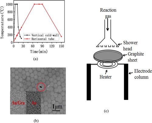
And a fascinating phenomenon for the VCW-CVD is that even if the reaction time was shorted down to 1 min, the continuous graphene films can still be formed. To verify the integrity of the graphene films prepared by VCW-CVD, the graphene films were transferred to the nanocolumn array with a diameter of 500 nm shown in . It can be found that the film was continuous except the circle place caused by the process of transfer. The illustration shows nanocolumn array with graphene transferred on the left and no graphene on the right. The Au film with 30 nm was sputtered on the nanocolumn array. It can be seen that the gold film can be completely retained on nanocolumn array with graphene, while there is no gold film formed on the nanocolumn array without graphene. It could be inferred that the graphene film prepared by the VCW-CVD has still very good continuity although with only one minute of reaction time.
Continuous graphene film grown by low pressure HT-CVD usually take more than tens of minutes to complete which is because of the different modes of ventilation. As shown in , the gas flow direction of HT-CVD is parallel to the sample, while the gas flow direction of the VCW-CVD is vertical to the sample. Hence, the flux of reaction atoms reaching sample in the VCW-CVD is much larger than flux in the HT-CVD in the same gas flow rate. So the former reaction time is much smaller than the later one. Does the rapid reaction makes the quality of the graphene films decline? It will be revealed by the measurement results.
In terms of the characterisation method of graphene layers, Raman spectra with unique advantage and perfect Lorentz peak type of second-order Raman peak (2D peak, near 2700 cm−1) are the simple and effective method for determining single-layer graphene. Raman spectroscopy is one of the effective characterisation methods about the quality of graphene, meanwhile it is also primary characterisation methods in this article. In order to ensure that Raman spectra accurately reflect the quality of graphene growth, the samples tested by Raman spectroscopy in this article were all on Cu substrate without transfer. Hence, the baseline of Raman curve is not horizontal curve. But it has no impact on determining the quality of graphene by Raman spectroscopy.
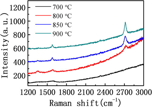
Because of the different heating modes of the VCW-CVD and HT-CVD, which are mainly the heat conduction and thermal radiation, respectively, thus for VCW-CVD, the quality of graphene influenced by the reaction temperature was studied in this article at first. The different growth temperature was set up as 700, 800, 850 and 900 °C, respectively, and the catalysts are copper foils with the purity of 99.999% and 25 microns thick. After completing the growth of samples, the samples are tested by Raman spectroscopy. The results of the test are shown in . In , it is obvious that the result of test by Raman spectroscopy has no 2D peak at a growth temperature of 700 °C, which indicates that double phonon scattering resonance is very weak in the grown graphene and the two-dimensional feature of the samples is very poor. But it can be seen that there are G peak which is caused by the internal vibration of carbon atoms, and the half height width of G peak is large. In addition, there is no obvious D peak in the Raman spectra of the samples, but it has obvious bulge in the wave band of D peak, which shows a lot of chaotic vibration in the sample. So it can be determined that the sample is a kind of amorphous carbon film, or nano graphite sediment with very small single-crystal and two-dimensional feature. When reaction temperature increases up to 800 °C, it can be clearly observed D, G, 2D peaks in the Raman spectra, which show that the prepared graphene is a two-dimensional graphene. The intensity ratio of G peak and D peak is about 1:1, which indicates the graphene contains many defects prepared at a growth temperature of 800 °C. The possible reason is that the small size single crystal in graphene film caused lots of crystal boundaries and the carbon atom in graphene is disordered. The intensity ratio of 2D peak and G peak is about 1.3:1, which indicates the sample has pretty good two-dimensional feature at the temperature of 800 °C. Generally when the intensity ratio of 2D peak and G peak is greater than 1.5:1, the graphene film can be viewed as single-layer graphene. The sample grown at the temperature of 800 °C was close to single-layer graphene. Meanwhile it can be seen that there are weak D peak, relatively obvious G peak and stronger 2D peak by Raman spectra of sample at the temperature of 850 °C. And the intensity rate of D and G peak is about 1:2.6, which showed that the ordering degree of carbon atom in graphene is higher. The intensity ratio of 2D peak and G peak is about 2.8:1, and the ratio has been far more than 1.5:1. Thus according to the measured results of the sample, it can be proved that the samples have very good two-dimensional feature. While the heating temperature is 900 °C, there is almost no D peak in Raman spectra of samples in and the intensity ratio of 2D peak and G peak is about 3.2:1. It shows that the relative strength of G peak at the temperature of 900 °C is obviously enhanced compared with the relative strength of G peak at the temperature of 850 °C. According to the above data analysis, the results show that the prepared graphene samples at the temperature of 900 °C have less single-crystal boundary, fewer defects, higher crystallinity and good quality.
Figure 2. Raman spectra of graphene films prepared by the VCW-CVD at 700, 800, 850 and 900 °C (copper substrate).
In order to further explore the optimum growth conditions for the preparation of graphene by VCW-CVD, the reaction temperature was increased to 1000 °C. Raman spectrum of the prepared sample is shown in . Compared with the results at the reaction temperature of 900 °C, it shows that the curve at 1300 cm−1 is more flat and we cannot distinguish the signal of the D-peak from . Meanwhile, the intensity ratio of G peak and 2D peak is about 1:3.1, which is similar to the results at the reaction temperature of 900 °C. To further study the effect of methane concentration on the growth of graphene, the flow rate of methane was increased at the reaction temperature of 1000 °C, the original methane at the flow rate of 10 sccm was increased to 20 sccm, and the prepared samples were tested by Raman spectroscopy. The test results are shown in . From the test results of Raman spectroscopy at the different flow rate, it can be seen that the change about flow rate of methane have little effect on measurements of Raman spectroscopy. Then the flow rate of methane was increased to 60 sccm and it was found same as the test results. Therefore, it can be concluded that the higher the reaction temperature, the better the quality of the prepared graphene samples. And the graphene can be formed at the reaction temperature of 800 °C with more defects and low two dimensions. The monolayer graphene samples with the higher two dimensions can be formed at the reaction temperature of 850 °C, while there are still some partial defects. At the reaction temperature of 900 °C, it could have been able to form the monolayer graphene with better quality, and at this time the D peak of Raman spectrum has been very weak, with very few defects. Finally, the graphene film with very high quality can be prepared by VCW-CVD at the reaction temperature of 1000 °C.
Figure 3. Raman spectra of graphene films under different growth conditions (copper substrate): (a) the different flow rate of methane at the temperature of 1000 °C, 10 sccm, 20 sccm respectively. (b) 99.8% and 99.999% copper foil at the temperature of 900 °C.
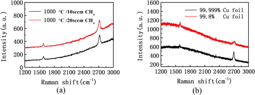
In order to prepare the graphene samples with high quality, we further validated the effect of purity of copper foil on the preparation of graphene by VCW-CVD. Under the same growth conditions, the reaction temperature was 1000 °C, and the growth of graphene was carried out with copper foil having a purity of 99.8% and 99.999% copper foil, respectively. The measurement results of Raman spectroscopy whose laser wavelength was 532 nm are as shown in . It can be seen that the two groups of measurement results show no obvious signal of D peak, but there is the clear signal of G peak and the great differences about relative intensity of 2D peak. In addition, the intensity ratio of G peak and 2D peak is about 1:0.8 and 1:3.1, respectively as shown in . It shows that the purity of copper foil has a certain effect on the Raman properties of graphene grown by VCW-CVD. And the higher the purity is, the better the two-dimensional and monolayer property of the graphene are. In the experimental results, the proportion of elevated methane has little impact on the quality of graphene, at the same time it also shows the copper foil is self-limiting in the process of catalytic growth about graphene, which indicates that the layer of graphene grown on the surface of copper foil can further prevent the catalytic action of copper foil. In other words, the copper foil is easier to grow monolayer graphene as the catalyst. Hence, it can be inferred that there are incomplete copper atoms on the surface of low purity copper foil, so it is possible to deposit multiple layers of graphene or carbon atoms in the area of non-copper atoms, affecting the monolayer characteristics of the whole growth of graphene film.
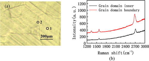
In the process of graphene growth, due to the role of high temperature, the atoms in the copper foil will be rearranged to form a domain, as shown in . The above measures were tried to avoid the boundary. In addition, we selected two different points on the same sample for Raman spectroscopy in order to research the effect of the position of crystal domain on the graphene film. As shown in , point 1 is the one point at the inside of crystal domain, and point 2 is the other on the boundary of crystal domain. Raman spectrum of two points is shown in . From the test results of the two, the signal of G peak and 2D peak is very strong and the intensity ratio of G peak and 2D peak is also relatively close, which indicates that the graphene film has very great monolayer feature at the two points. However, there are very obvious D peak in the test results of point 2, whose reason is that the growth of graphene at the junction of crystal domain has a large amount of boundaries. It is reported [Citation18,Citation19] that the atomic arrangement of the single-crystal graphene is the same in a copper crystal domain after CVD growth, which is to say the atomic arrangement of the graphene is usually different at the different junctions of copper crystal domains. Hence, a large number of graphene boundaries are easily generated at the boundaries of the copper crystal domain, resulting in the strong signal of D peak. The results of this experiment are consistent with some paper reported before [Citation20,Citation21].
Figure 4. (a) The single-crystal graphene grown on the copper foil. (b) Raman spectra of different positions on the copper foil.
In order to further verify the difference of quality between the graphene prepared by the VCW-CVD method and the graphene prepared by the HT-CVD method, the two samples grown at the temperature of 1000 °C was selected to compare the thermal stability and the transmittance. In addition, the conductivity of graphene was used to reflect the thermal stability in this article.
Two kinds of graphene were respectively made into three groups of devices shown in , and the areas between the two parallel electrodes are square graphene with the size of 200 μm × 200 μm. The first group was without any treatment. The second group was heated at a temperature of 300 °C for 1 h in the air. The third group was heated at 400 °C for 1 h in the air. And then the current and voltage of the three group devices were tested between the two electrodes. Due to the small contact resistance between the graphene and the metal, the small contact resistance can be negligible and the square resistance value will be obtained from the I–V curves. The I–V curves in respectively correspond to the graphene prepared by the VCW-CVD method and the ordinary HT-CVD method. From the I–V curves, it can be seen that the value of square resistance of the first samples is 1269 Ω/□ and 1337 Ω/□, respectively. The second ones are respectively 1231 Ω/□ and 1250 Ω/□. The third ones are respectively 2747 Ω/□ and 7142 Ω/□. In addition, the conductivity of graphene prepared by the two methods is not obviously changed at 300 °C, but the conductivity has a large decrease at 400 °C. The graphene prepared by the two methods is basically the same at high temperature oxidation resistance. There are two kinds of oxidation mechanisms of graphene in the air. One is that the atoms on the graphene atomic network react with the oxygen in the air. The other is that the atoms react with oxygen in the air at the edge of the graphene atomic network, which is on the boundary of the single-crystal graphene and the defects. And the second mechanism of reaction is more possibly to occur because of low broken bond energy in the process of oxidation. In a word, the process of general graphene oxidation often occurs on the boundary of the single-crystal graphene.
Figure 5. (a) The thermal stability test results of graphene prepared by VCW-CVD; (b) the thermal stability test results of graphene prepared by HT-CVD; (c) the transmittance test results of grapheme prepared by VCW-CVD and HT-CVD; (d) the device structure diagram of square resistance test.
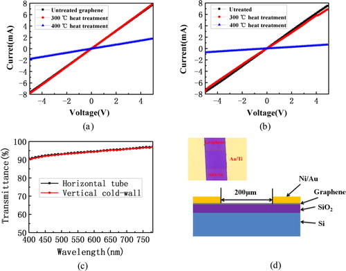
The curves in show the transmittance of the two graphene films. Under the same transfer conditions, we find that the transmittance of the two graphene films remains essentially the same. The transmittance of graphene is lower in the short band, reaching to 97.5% at the wave length of 800 nm, which is close to the theoretical value of 97.7%. The results are in good agreement with the related reports.
4. Conclusion
In this article, monolayer layer graphene films prepared by VCW-CVD method were investigated. The effects of reaction temperature, substrate purity and methane concentration in the reaction gas on the quality of the monolayer graphene film were investigated. Coming to the conclusion that the higher the temperature and the substrate more pure, the quality of graphene is better; in a certain range of concentration of methane, for the VCW-CVD preparation of graphene, methane concentration has no obvious influence on the quality of graphene films. In order to further prove the quality of single layer graphene prepared by vertical VCW-CVD method, the size of graphene single crystal was qualitatively measured and found that the size of its single crystal coincided with that of the HT-CVD. At the same time, the oxidation resistance and transmittance of the graphene prepared by the two CVD methods have been tested, and no obvious difference has been found between the two. Therefore, there is no obvious difference between the graphene prepared from the VCW-CVD method and the most commonly used HT-CVD method. The preparation time of graphene by VCW-CVD method is only 1/6 of the HT-CVD method. It takes only about 25 min.
Disclosure statement
No potential conflict of interest was reported by the authors.
Additional information
Funding
Notes on contributors
Kun Xu
Kun Xu received the bachelor’s degree in electronic engineering from Xidian University, Xi'an, China, in 2010, the Ph.D. degree from the Beijing University of Technology, Beijing, China, in 2015. He (corresponding author) is currently a associate professor with the Zhengzhou University of Aeronautics. His current research interests include preparation of graphene and application of graphene in semiconductor optoelectronic devices.
References
- Novoselov KS, Geim KA, Morozov VS, et al. Electric field effect in atomically thin carbon films. Science. 2004;306(5296):666–669.
- Bonaccorso F, Sun Z, Hasan T, et al. Graphene photonics and optoelectronics. Nat Photon. 2010;4(9):611–622.
- Choi D, Kuru C, Choi C, et al. Unusually high optical transparency in hexagonal nanopatterned graphene with enhanced conductivity by chemical doping. Small. 2015;11(26):3143–3152.
- Wang L, Liu W, Zhang Y, et al. Graphene-based transparent conductive electrodes for GaN-based light emitting diodes: Challenges and countermeasures. Nano Energy. 2015;12:419–436.
- Wu C, Liu F, Liu B, et al. Enhanced opto-electrical properties of graphene electrode InGaN/GaN LEDs with a NiOx inter-layer. Solid-State Electron. 2015;109:47–51.
- Meng J, Liu X, Zhang X, et al. Interface engineering for highly efficient graphene-on-silicon Schottky junction solar cells by introducing a hexagonal boron nitride interlayer. Nano Energy. 2016;28:44–50.
- Kim BJ, Hwang E, Kang MS, et al. Electrolyte-gated graphene Schottky barrier transistors. Adv Mater. 2015;27(39):5875–5881.
- Peter WS, Jan-Ingo F, Eli AS. Epitaxial graphene on ruthenium. Nat Mater. 2008;7:406–411.
- Xu K, Xie Y, Ma H, et al. ZnO nanorods/graphene/Ni/Au hybrid structures as transparent conductive layer in GaN LED for low work voltage and high light extraction. Solid-State Electron. 2016;126:5–9.
- Xu K, Xu C, Xie Y, et al. GaN nanorod light emitting diodes with suspended graphene transparent electrodes grown by rapid chemical vapor deposition. Appl Phys Lett. 2013;103(22):222105.
- Xu K, Xu C, Xie Y, et al. Graphene GaN-based Schottky ultraviolet detectors. IEEE Trans Electron Devices. 2015;62(9):2802–2808.
- Kun X, Chen X, Jun D, et al. Graphene transparent electrodes grown by rapid chemical vapor deposition with ultrathin indium tin oxide contact layers for GaN light emitting diodes. Appl Phys Lett. 2013;102(16):162102.
- Li X, Cai W, Colombo L, et al. Evolution of graphene growth on Ni and Cu by carbon isotope labeling. Nano Lett. 2009;9(12):4268–4272.
- Bae S, Kim H, Lee Y, et al. Roll-to-roll production of 30-inch graphene films for transparent electrodes. Nat Nanotechnol. 2010;5(8):574–578.
- Miseikis V, Convertino D, Mishra N, et al. Rapid CVD growth of millimetre-sized single crystal graphene using a cold-wall reactor. 2D Materials. 2015;2(1):01400.
- Bointon TH, Barnes MD, Russo S, et al. High quality monolayer graphene synthesized by resistive heating cold wall chemical vapor deposition. Adv Mater Weinheim. 2015;27(28):4200–4206.
- Arjmandi-Tash H, Lebedev N, van Deursen PMG, et al. Hybrid cold and hot-wall reaction chamber for the rapid synthesis of uniform graphene. Carbon. 2017;118:438–442.
- Hsieh Y, Chen D, Chiang W, et al. Recrystallization of copper at a solid interface for improved CVD graphene growth. RSC Adv. 2017;7(7):3736–3740.
- Li J, Wang G, Geng H, et al. CVD growth of graphene on NiTi alloy for enhanced biological activity. ACS Appl Mater Interfaces. 2015;7(36):19876–19881.
- Wu J, Xu H, Zhang J. Raman spectroscopy of graphene. Acta Chim Sin. 2014;72(3):301.
- Pang J, Bachmatiuk A, Ibrahim I, et al. CVD growth of 1D and 2D sp2 carbon nanomaterials. J Mater Sci. 2016;51(2):640–667.