Abstract
A new method for fabricating metal nanostructures, called ‘the selective metal nanoscale etch method (SMNEM)’, was developed. The SMNEM consists of a galvanic displacement and selective etching process. The process was found to be simple and produced a uniform surface with a self-controlled etch rate of 32.2 ± 2.1 nm per cycle at a temperature and immersion time of 75°C and 3 min, respectively. Since it is a wet chemical process, SMNEM provides high throughput and low temperature etching which is compatible with conventional semiconductor processes. Various metal nanostructures, such as nanostairs, nanogratings, and nanowires were produced using SMNEM.
1. Introduction
Metal structures have superior strength and electrical conductivity, and are used in a wide variety of semiconductor and sensor industrial applications, including semiconductor metal lines, micro electro-mechanical system (MEMS) structures, and nano electro-mechanical system (NEMS) structures. In particular, metal nanostructures are applied widely in the fields of nano-electronics, optical-electronics, chemistry and biological sensors, on account of their size and shape-dependent variations in electromagnetic properties, thermal conductivity, and depending on their mechanical characteristics Citation1–4. Grigorenko et al. used gold metal pillars with a novel geometry that demonstrated metamaterial properties in the visible spectrum Citation1. Ozbay published a review article showing that the interaction of light with matter in nanostructured metallic structures can overcome the limitations of electronics and photonics, which has led a new branch called plasmonics Citation2. Nanostructured metal–oxide–metal diodes have also been used to detect infrared and millimeter wavelengths with high advantages in polarisation dependence, tuneability, and a potential rapid time response Citation3. Furthermore, the mechanical hardness of a metal is mainly used as a mask to fabricate complicated polymer nanostructures Citation4.
Methods for manufacturing such metal nanostructures can be classified in the following 4 ways: deposition through a nanopatterned polymer as a mould, electroplating using a nanometer-scale, wet etching, and dry etching with plasma energy. When depositing through a nanopatterned polymer, a metal is deposited through a nanopatterned polymer as a mould, which is then lifted off to obtain free-standing metal structures Citation5. During lift-off, the pattern might be removed along with the photoresist and metal residue with different heights and thicknesses can be left at the side walls. Electroplating using a nanometer-scale mould can produce metal nanostructures Citation6. However, a mould on nanometer-scale is needed and an electrode must always be connected. In addition, a uniform pattern size or chemical mechanical polishing (CMP) is generally performed because the plating thickness can vary according to the pattern size. Wet etching by dipping into wet chemicals is simple and inexpensive, and is used widely in MEMS processes Citation7. However, when wet etching is used, the exposed portion of the metal structure is always etched isotropically to have round-shaped side surface, rather than vertical planes. Dry etching with plasma energy can be difficult to perform due to the metal strength, and there are many limitations with this process Citation8. Structures other than the desired metal structure might be etched under the strict etching conditions. Furthermore, all these methods for achieving three-dimensional structures can be limited by these complicate processes.
In this study, a new method for fabricating metal nanostructures, called ‘the selective metal nanoscale etch method (SMNEM)’, was developed to solve the above problems. Various metal nanostructures such as nanostairs, nanogratings, and nanowires were produced using the SMNEM.
2. The selective metal nanoscale etch method
Selective metal nanoscale etch method consists of photolithography, galvanic displacement, and a selective etching process. SMNEM was accomplished through four fundamental steps Citation9:
-
deposition of a metal film or structures onto a substrate,
-
application of a patterned polymer resist onto the metal film or structure,
-
immersion of the substrate into an electroless plating solution (diluted metal salt), where the REDOX process or galvanic exchange causes the displacement of each metal Citation10, and
-
selective peel-off or removal of a displaced metal through a metal etchant.
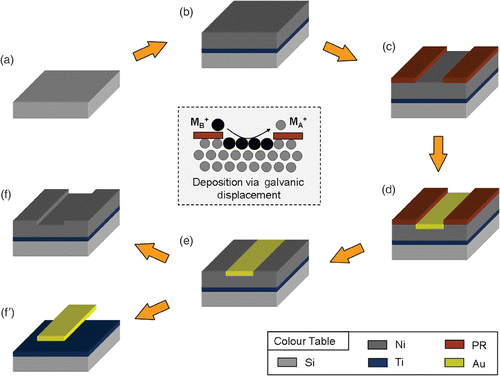
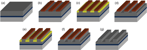
shows a schematic diagram of the SMNEM for generating a metal nanoscale structure. The entire SMNEM is only a wet chemical process. Therefore, silicon, compound semiconductor, glass, and flexible polymer substrates can be used. A p-type Si(100) wafer was used as the substrate material (). As shown in , Ti(200 Å) and Ni(2000 Å) metal layers were deposited onto a Si substrate by thermal evaporation. Ti layer was used as an adhesive layer. A Ni layer was used because of its high-ionization tendency, which makes the REDOX process easy and conventional utility in the semiconductor process. The Ni replacing metal film can be changed to steel, zinc, aluminum, and copper Citation11. After metal deposition, a AZ6612K photoresist was patterned using a MA6 aligner to mask the Ni layer surface (). The etching area and position can be defined easily and precisely using lithographical methods on the substrate. Some nanolithographic equipments such as E-beam or nano-imprinting lithography can be used if more precise patterns down to a few nanometer size are required. Hence, the lithographical resolution constrains the lateral etching accuracy. Subsequently, the exposed Ni atoms were replaced with Au metal by immersing the substrate into an electroless plating solution containing Au metal salt (KAu(CN)2(aqua)) (). The replaced metal can also change with a more noble metal such as silver, cadmium, copper, and zinc. The electroless plating solution provided by CNCtech Co., Ltd. contained 2 gL−1 of Au in an ELECTLESS FX basic solution and the pH was adjusted to 4.7 using a pH Basic-A solution. Galvanic replacement of each metal atom was performed by dipping into this solution. The replacement time was 3 min and the process temperature was 75°C. The photoresist was removed by acetone (). Finally, a selective Au etchant (Au-5) removed the Au layer through physically self-controlled etch stop and etching depth (). The selectivity of the Ni metal film dipped into Au etchant was checked to confirm that no attack had occurred within 1 h Citation12. Diluted Au-5 (Au-5 : deionised water = 1 : 10) was used to etch the displaced Au layer for 30 s. On the other hand, a Ni etchant enabled the fabrication of Au thin film or suspended structures, as shown in .
Figure 1. The process flow of the SMNEM. (a) Substrate preparation, (b) Ti/Ni layers deposition, (c) photoresist patterning, (d) electroless plating or galvanic displacement, (e) photoresist removal, (f) selective metal etching.
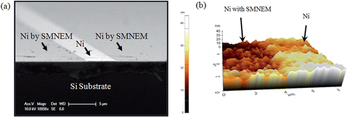
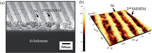
shows the results of SMNEM. Scanning electron microscopy (SEM) showed that Ni layer masked by the photoresist had a ridge structure with a 30 nm height based on the etching site (). The length and width of the ridge area was defined using a photolithographic mask pattern. shows an atomic force microscopy (AFM) image after SMNEM. An AFM (XE-100, PSIA) in contact mode was used to measure the etching depth or etch rate of SMNEM and examine the surface roughness. The mean etching depth of SMNEM was 32.3 ± 2 nm. The surface root-mean-square (RMS) roughness of the etched area and original Ni surface were measured to be 6.9 ± 2 nm and 9.5 ± 2 nm, respectively. Therefore, SMNEM produced a smooth surface.
Figure 2. (a) SEM image and (b) 3D AFM image of a Ni metal ridge after SMNEM.
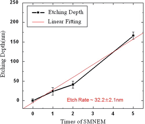
shows the results of the number of SMNEM times versus the etching depth for three-dimensional metallic nanostructures. The SMNEM process was repeated and the etch rate per number of SMNEM cycles was measured. The samples used to obtain this data were fabricated without photoresist patterning. The etching depth was calculated by subtracting the remaining thickness from the original thickness. A straight line was obtained when the etch rate was plotted with respect to the number of SMNEM cycles, which indicated 32.2 ± 2 nm per cycle. Therefore, a constant etching rate per number of SMNEM cycles shows that the displacement thickness by electroless plating is self-controlled by fixing the time and process temperature.
Figure 3. The number of SMNEM cycles versus the Ni etching depth after Au selective etching.
3. The application of SMNEM
From a size reduction process by utilising the self-saturated etching thickness, three-dimensional metal nanostructures, such as nanostairs, nanogratings, and nanowires, could be fabricated using SMNEM.
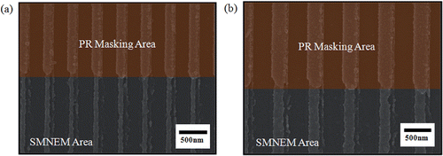
Nanostairs with a micrometer width and nanometer height were obtained. shows the results of the fabricated nanostairs. The experiment was carried out using the same conditions described in the SMNEM chapter. SMNEM was repeated by extending the photoresist masks (). The first height of the nanostair was 30 ± 3 nm and the second height of the nanostairs was 34 ± 4 nm. Another design was adjusted by aligning the first Ni pattern and the third mask, as shown in . When the photoresist were not tightly adhered to the Ni surface, galvanic displacement can occur inside the gap between the photoresist and the Ni layer. shows a very thin rounded mark patterned on the initial Ni surface during SMNEM. Thus, nanometer wide stairs can be fabricated by E-beam lithography and a nanometer height can be produced by SMNEM.
Figure 4. (a) SEM image and (b) 3D AFM image of a thickness controlled Ni step.
A SMNEM was also used to adjust the metal nanograting depth. The metal nanogratings can be used as a mould to fabricate polymer optical gratings or for surface plasmon resonance (SPR) structures. shows process for fabricating metal nanogratings. After the Ti(200 Å) and Ni(3000 Å) metal layers had been deposited onto Si substrate using an e-beam evaporator (), a dilute AZ6612K solution (AZ6612K : AZ1500 = 3 : 7) was spin-coated on the Ni layers. The thickness of the diluted AZ6612K was 200 nm. The photoresist was then patterned using a holographic lithography system that determined the period of the nanogratings (). After the photolithographic process, the substrate was immersed into dilute Au metal salt (KAu(CN)2(aqua)), which allowed the exposed Ni metal to be replaced with Au (). A selective Au etchant (diluted Au-5) removed the Au layer (). The replacement and selective etching process was repeated to obtain the precise grating depth with the highest coupling efficiency (). Finally, the photoresist was removed soon after the target grating depth had been attained ().
Figure 5. The process flow of Ni nanogratings fabricated by holographic lithography and two SMNEM cycles. (a) Ti/Ni layers deposition on the substrate, (b) holographic lithography, (c–f) two SMNEM cycles, (g) photoresist removing.
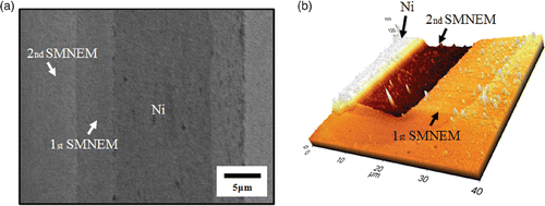
shows SEM and AFM images of the Ni nanogratings. As shown in , the grating period of the Ni nanogratings was 400 nm and the duty was half at the highest efficiency. AFM in contact mode was used to measure the etching depth of Ni nanogratings, as shown in . Because the replacement time was reduced from 3 min to 2 min and maintained at 75°C in a double boiler, the etching depth after performing SMNEM once and twice was 23 ± 5 nm and 47 ± 4 nm, respectively.
Figure 6. (a) SEM image and (b) 3D AFM image of thickness controlled Ni nanogratings.
Nickel nanowires can be fabricated by SMNEM. shows a schematic diagram of the methodology used to fabricate the Ni metal nanowires. Ni submicron wires were pre-patterned on a Si3N4 substrate by e-beam lithography followed by a lift-off process (). The dimension of the Ni submicron wires was 200 nm in height, 200 nm or 300 nm in width, and 70 µm in length. An AZ6612K Photoresist was spin-coated on the Ni submicron wires. The photoresist was the patterned and developed to confine the area for applying SMNEM (). After the photolithographic process, SMNEM, which is the combination of galvanic displacement () and selective Au etching (), was performed. Finally, the photoresist was removed (). The experiment was carried out under the same conditions reported in the SMNEM chapter with the exception that the immersion time and processing temperature was 3 min and 80°C, respectively. shows the result of reducing the size of Ni nanowires. shows that the initial width and width of the reducing Ni nanowires was 184 nm and 89 nm, respectively. The width of the thicker Ni nanowires decreased from 289 nm to 184 nm ().
Figure 7. The process flow of 3D Ni nanowires fabricated by SMNEM. (a) Ni nanowire formation by E-beam lithography and lift-off, (b) photoresist patterning, (c–d) SMNEM, (e) photoresist removing.
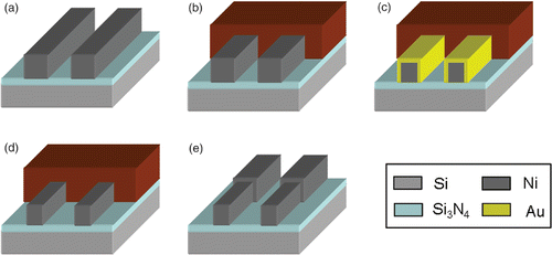
Figure 8. SEM images of the 3D Ni nanowires starting from (a) 200 nm Ni nanowires and (b) 300 nm Ni nanowires.
Overall, the etching depth for fabricating various metal nanostructures can be controlled precisely by changing the process temperature and immersion time.
4. Conclusion
This article introduced a new SMNEM and its potential applications. A Ni metal layer was etched uniformly on the nanoscale. This layer has potential applications to 3D metal nanopatterning. SMNEM provides a controllable etching depth, depending on the process temperature and immersion time, by repeating the process. Moreover, the proposed method can be easily applied to produce various new 3D metal nanostructures such as nanostairs, nanogratings, and nanowires. Therefore, SMNEM is a simple and cost-effective process of nanofabrication.
Acknowledgment
This work was supported by the Korea Institute of Science and Technology Basic Research Grant.
References
- Grigorenko , AN . 2005 . Nanofabricated media with negative permeability at visible frequencies . Nature , 438 : 335 – 338 .
- Ozbay , E . 2006 . Plasmonics: merging photonics and electronics at nanoscale dimensions . Science , 311 : 189 – 193 .
- Alda , J . 2005 . Optical antennas for nano-photonic applications . Nanotechnology , 16 : S230 – S234 .
- Yu , Z . 2003 . Fabrication of large area subwavelength antireflection structures on Si using trilayer resist nanoimprint lithography and liftoff . J. Vac. Sci. Technol. B , 21 : 2874 – 2877 .
- Vieu , C . 2000 . Electron beam lithography: resolution limits and applications . Appl. Surf. Sci. , 164 : 111 – 117 .
- Kline , TR . 2006 . Template-grown metal nanowires . Inorg. Chem. , 45 : 7555 – 7565 .
- Kovacs , GTA . 2000 . Micromachined Transducers Sourcebook , Singapore : WCB/McGraw-Hill .
- Savolainen , M . 2004 . Ion beam sputtering for progressive reduction of nanostructures dimensions . Appl. Phys. A , 79 : 1769 – 1773 .
- Lee , BC and Moon , S . Method for manufacturing metal structure and carbon nanotube by using immersion plating , PCT patent pending, Patent Number PCT/KR2006/004130
- Watanabe , T . 2004 . Nano-Plating; Microstructure Control Theory of Plated Film and Data Base of Plated Film Microstructure , Oxford : Elsevier .
- Mallory , GO and Hajdu , JB . 1990 . Electroless Plating: Fundamentals and Applications , Orlando : American Electroplaters and Surface Finishers Society .
- Williams , KR , Gupta , K and Wasilik , M . 2003 . Etch rates for micromachining processing–Part II . J. MEMS , 12 : 761 – 778 .